

Datasheet LM2930T-8.0, LM2930SX-8.0, LM2930S-8.0, LM2930S-5.0, LM2930-8.0MWC Datasheet (NSC)
...Page 1
LM2930
3-Terminal Positive Regulator
General Description
The LM2930 3-terminal positive regulator features an ability
to source 150 mA of output current with an input-output differential of 0.6V or less. Efficient use of low input voltages
obtained, for example, from an automotive battery during
cold crank conditions, allows 5V circuitry to be properly powered with supply voltages as low as 5.6V. Familiar regulator
features such as current limit and thermal overload protection are also provided.
Designed originally for automotive applications, the LM2930
and all regulated circuitry are protected from reverse battery
installations or 2 battery jumps. During line transients, such
as a load dump (40V) when the input voltage to the regulator
can momentarily exceed the specified maximum operating
voltage, the regulator will automatically shut down to protect
both internal circuits and the load. The LM2930 cannot be
harmed by temporary mirror-image insertion.
Fixed outputs of 5V and 8V are available in the plastic
TO-220 and TO-263 power packages.
Features
n Input-output differential less than 0.6V
n Output current in excess of 150 mA
n Reverse battery protection
n 40V load dump protection
n Internal short circuit current limit
n Internal thermal overload protection
n Mirror-image insertion protection
n P
+
Product Enhancement tested
Voltage Range
LM2930T-5.0: 5V
LM2930T-8.0: 8V
LM2930S-5.0: 5V
LM2930S-8.0: 8V
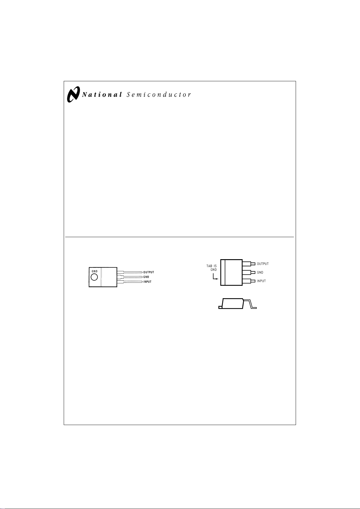
Connection Diagrams
(TO-220)
Plastic Package
DS005539-1
Front View
Order Number LM2930T-5.0 or LM2930T-8.0
See NS Package Number T03B
(TO-263)
Plastic Surface-Mount Package
DS005539-7
Top View
DS005539-8
Side View
Order Number LM2930S-5.0 or LM2930S-8.0
See NS Package Number TS3B
April 1998
LM2930 3-Terminal Positive Regulator
© 1998 National Semiconductor Corporation DS005539 www.national.com
Page 2
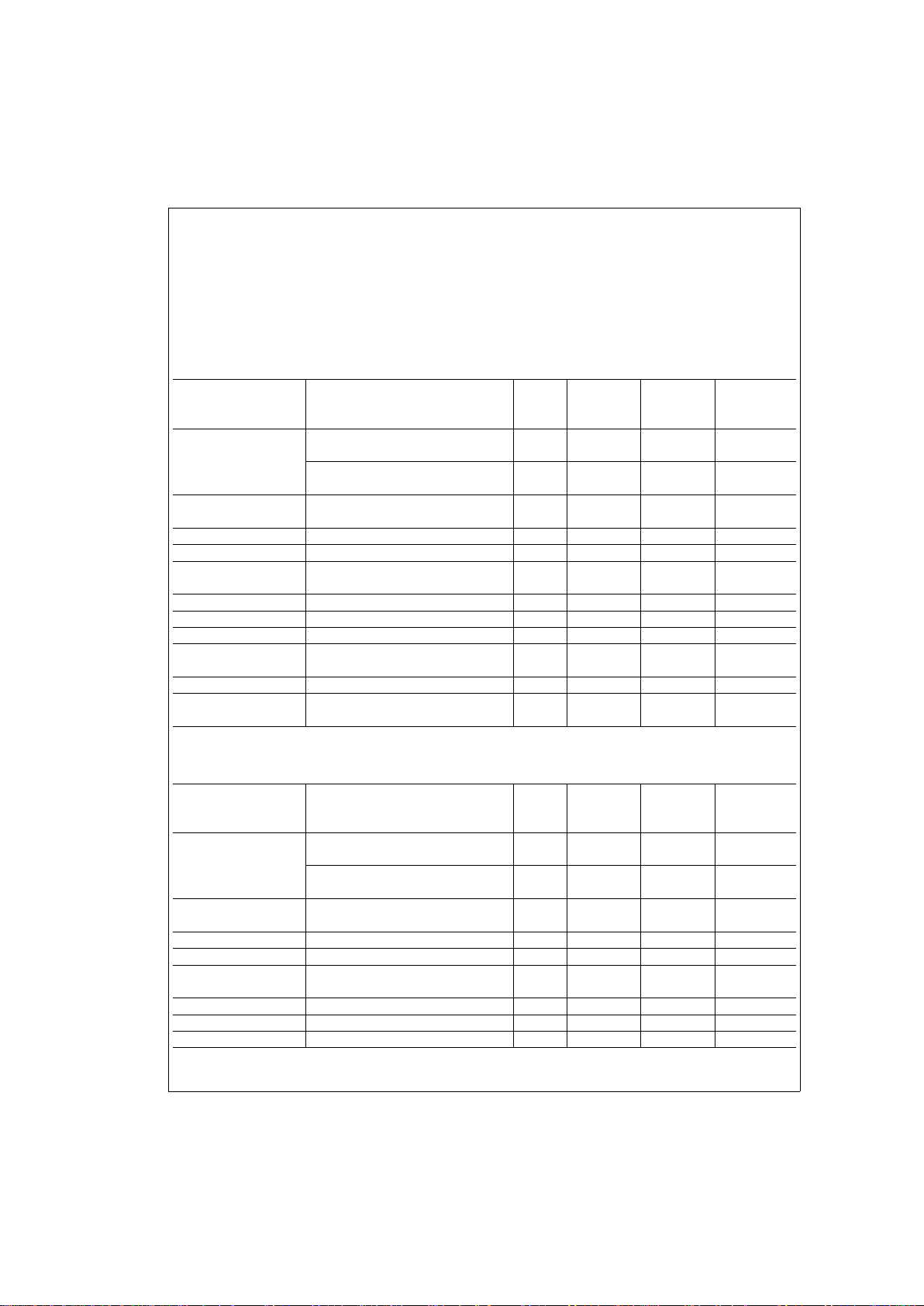
Absolute Maximum Ratings (Note 1)
If Military/Aerospace specified devices are required,
please contact the National Semiconductor Sales Office/
Distributors for availability and specifications.
Input Voltage
Operating Range 26V
Overvoltage Protection 40V
Reverse Voltage (100 ms) −12V
Reverse Voltage (DC) −6V
Internal Power Dissipation (Note 2) Internally Limited
Operating Temperature Range −40˚C to +85˚C
Maximum Junction Temperature 125˚C
Storage Temperature Range −65˚C to +150˚C
Lead Temp. (Soldering, 10 seconds) 230˚C
Electrical Characteristics (Note 3)
LM2930-5.0 V
IN
=
14V, I
O
=
150 mA, T
j
=
25˚C (Note 6), C2=10 µF, unless otherwise specified
Tested Design
Parameter Conditions Typ Limit Limit Unit
(Note 4) (Note 5)
Output Voltage 5 5.3 V
MAX
4.7 V
MIN
6V≤VIN≤26V, 5 mA≤IO≤150 mA 5.5 V
MAX
−40˚C≤TJ≤125˚C 4.5 V
MIN
Line Regulation 9V≤VIN≤16V, I
O
=
5 mA 7 25 mV
MAX
6V≤VIN≤26V, I
O
=
5mA 30 80 mV
MAX
Load Regulation 5 mA≤IO≤150 mA 14 50 mV
MAX
Output Impedance 100 mADC&10mA
rms
, 100 Hz−10 kHz 200 mΩ
Quiescent Current I
O
=
10 mA 4 7 mA
MAX
I
O
=
150 mA 18 40 mA
MAX
Output Noise Voltage 10 Hz−100 kHz 140 µV
rms
Long Term Stability 20 mV/1000 hr
Ripple Rejection f
O
=
120 Hz 56 dB
Current Limit 400 700 mA
MAX
150 mA
MIN
Dropout Voltage I
O
=
150 mA 0.32 0.6 V
MAX
Output Voltage Under −12V≤VIN≤40V, R
L
=
100Ω 5.5 V
MAX
Transient Conditions −0.3 V
MIN
Electrical Characteristics (Note 3)
LM2930-8.0 (V
IN
=
14V, I
O
=
150 mA, T
j
=
25˚C (Note 6), C2=10 µF, unless otherwise specified)
Tested Design
Parameter Conditions Typ Limit Limit Unit
(Note 4) (Note 5)
Output Voltage 8 8.5 V
MAX
7.5 V
MIN
9.4V≤VIN≤26V, 5 mA≤IO≤150 mA, 8.8 V
MAX
−40˚C≤TJ≤125˚C 7.2 V
MIN
Line Regulation 9.4V≤VIN≤16V, I
O
=
5mA 12 50 mV
MAX
9.4V≤VIN≤26V, I
O
=
5 mA 50 100 mV
MAX
Load Regulation 5 mA≤IO≤150 mA 25 50 mV
MAX
Output Impedance 100 mADC&10mA
rms
, 100 Hz−10 kHz 300 mΩ
Quiescent Current I
O
=
10 mA 4 7 mA
MAX
I
O
=
150 mA 18 40 mA
MAX
Output Noise Voltage 10 Hz−100 kHz 170 µV
rms
Long Term Stability 30 mV/1000 hr
Ripple Rejection f
O
=
120 Hz 52 dB
www.national.com 2
Page 3
Electrical Characteristics (Note 3) (Continued)
LM2930-8.0 (V
IN
=
14V, I
O
=
150 mA, T
j
=
25˚C (Note 6), C2=10 µF, unless otherwise specified)
Tested Design
Parameter Conditions Typ Limit Limit Unit
(Note 4) (Note 5)
Current Limit 400 700 mA
MAX
150 mA
MIN
Dropout Voltage I
O
=
150 mA 0.32 0.6 V
MAX
Output Voltage Under −12V≤VIN≤40V, R
L
=
100Ω 8.8 V
MAX
Transient Conditions −0.3 V
MIN
Note 1: Absolute Maximum Ratings indicate limits beyond which damage tothedevicemayoccur. Operating ratings indicate conditions for which the deviceisfunctional, butdonotguarantee specific performance limits. Electrical Characteristics state DC andAC electrical specifications under particular test conditions which guarantee specific performance limits. This assumes that the device is within the Operating Ratings. Specifications are not guaranteed for parameters where no limit is
given, however, the typical value is a good indication of device performance.
Note 2: Thermal resistance without a heat sink for junction to case temperature is 3˚C/W and for case to ambient temperature is 50˚C/W for the TO-220, 73˚C/W
for the TO-263. If the TO-263 package is used, the thermal resistance can be reduced by increasing the P.C.board copper area thermally connected to the package.
Using 0.5 square inches of copper area, θ
JA
is 50˚C/W; with 1 square inch of copper area, θJAis 37˚C/W; and with 1.6 or more square inches of copper area, θ
JA
is 32˚C/W.
Note 3: All characteristics are measured with a capacitor across the input of 0.1 µF and a capacitor across the output of 10 µF.All characteristics except noise voltage
and ripple rejection ratio are measured using pulse techniques (t
W
≤10 ms, duty cycle≤5%). Output voltage changes due to changes in internal temperature must be
taken into account separately.
Note 4: Guaranteed and 100%production tested.
Note 5: Guaranteed (but not 100%production tested) over the operating temperature and input current ranges. These limits are not used to calculate outgoing qual-
ity levels.
Note 6: To ensure constant junction temperature, low duty cycle pulse testing is used.
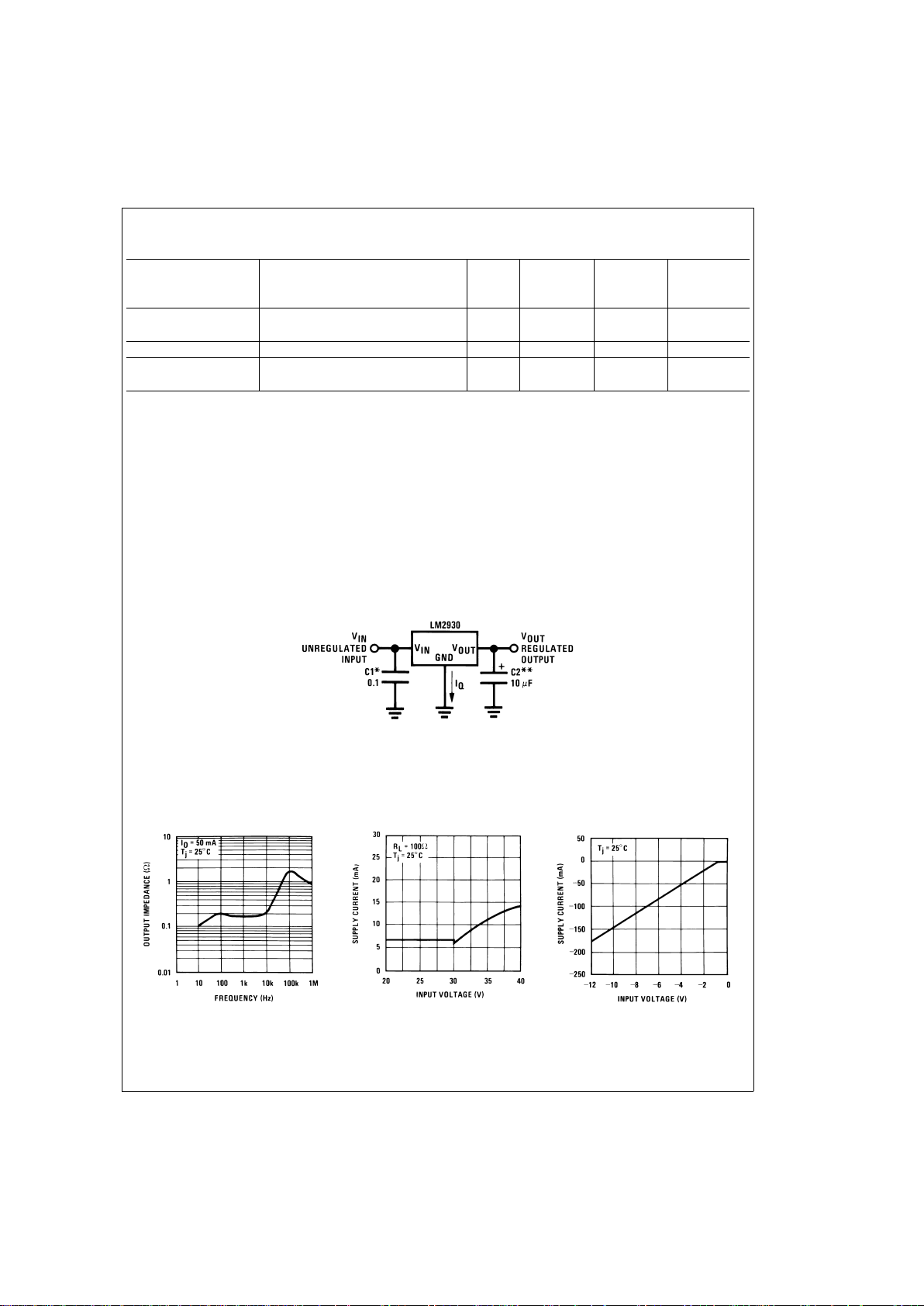
Typical Application
Typical Performance Characteristics
DS005539-5
*Required if regulator is located far from power supply filter.
*
*
C
OUT
must be at least 10 µF to maintain stability. May be increased without bound to maintain regulation during transients. Locate as close as possible to the
regulator. This capacitor must be rated over the same operating temperature range as the regulator. The equivalent series resistance (ESR) of this capacitor
should be less than 1Ω over the expected operating temperature range.
Output Impedance
DS005539-11
Overvoltage Supply Current
DS005539-12
Reverse Supply Current
DS005539-13
3 www.national.com
Page 4

Typical Performance Characteristics (Continued)
Output at Reverse
Supply
DS005539-14
Output at Overvoltage
DS005539-15
Output Voltage (Normalized
to 1V at T
j
=
25˚C)
DS005539-16
Dropout Voltage
DS005539-17
Dropout Voltage
DS005539-18
Low Voltage Behavior
DS005539-19
High Voltage Behavior
DS005539-20
Line Transient Response
DS005539-21
Load Transient Response
DS005539-22
www.national.com 4
Page 5

Typical Performance Characteristics (Continued)
Definition of Terms
Dropout Voltage: The input-output voltage differential at
which the circuit ceases to regulate against further reduction
in input voltage. Measured when the output voltage has
dropped 100 mV from the nominal value obtained at 14V input, dropout voltage is dependent upon load current and
junction temperature.
Input Voltage: The DC voltage applied to the input terminals
with respect to ground.
Input-Output Differential: The voltage difference between
the unregulated input voltage and the regulated output voltage for which the regulator will operate.
Line Regulation: The change in output voltage for a change
in the input voltage. The measurement is made under conditions of low dissipation or by using pulse techniques such
that the average chip temperature is not significantly affected.
Load Regulation: The change in output voltage for a
change in load current at constant chip temperature.
Long Term Stability: Output voltage stability under accelerated life-test conditions after 1000 hours with maximum
rated voltage and junction temperature.
Output Noise Voltage: The rms AC voltage at the output,
with constant load and no input ripple, measured over a
specified frequency range.
Quiescent Current: That part of the positive input current
that does not contribute to the positive load current. The
regulator ground lead current.
Ripple Rejection: The ratio of the peak-to-peak input ripple
voltage to the peak-to-peak output ripple voltage.
Temperature Stability of V
O
: The percentage change in
output voltage for a thermal variation from room temperature
to either temperature extreme.
Peak Output Current
DS005539-23
Quiescent Current
DS005539-24
Quiescent Current
DS005539-25
Quiescent Current
DS005539-26
Ripple Rejection
DS005539-27
Ripple Rejection
DS005539-28
Maximum Power
Dissipation (TO-220)
DS005539-6
5 www.national.com
Page 6

Definition of Terms (Continued)
Schematic Diagram
Maximum Power Dissipation
(TO-263) (Note 2)
DS005539-9
DS005539-10
www.national.com 6
Page 7

Physical Dimensions inches (millimeters) unless otherwise noted
TO-220 3-Lead Molded Package
Order Number LM2930T-5.0 or LM2930T-8.0
NS Package Number T03B
7 www.national.com
Page 8

Physical Dimensions inches (millimeters) unless otherwise noted (Continued)
LIFE SUPPORT POLICY
NATIONAL’S PRODUCTS ARE NOT AUTHORIZED FOR USE AS CRITICAL COMPONENTS IN LIFE SUPPORT DEVICES OR SYSTEMS WITHOUT THE EXPRESS WRITTEN APPROVAL OF THE PRESIDENT OF NATIONAL SEMICONDUCTOR CORPORATION. As used herein:
1. Life support devices or systems are devices or systems which, (a) are intended for surgical implant into
the body, or (b) support or sustain life, and whose failure to perform when properly used in accordance
with instructions for use provided in the labeling, can
be reasonably expected to result in a significant injury
to the user.
2. A critical component in any component of a life support
device or system whose failure to perform can be reasonably expected to cause the failure of the life support
device or system, or to affect its safety or effectiveness.
National Semiconductor
Corporation
Americas
Tel: 1-800-272-9959
Fax: 1-800-737-7018
Email: support@nsc.com
www.national.com
National Semiconductor
Europe
Fax: +49 (0) 1 80-530 85 86
Email: europe.support@nsc.com
Deutsch Tel: +49 (0) 1 80-530 85 85
English Tel: +49 (0) 1 80-532 78 32
Français Tel: +49 (0) 1 80-532 93 58
Italiano Tel: +49 (0) 1 80-534 16 80
National Semiconductor
Asia Pacific Customer
Response Group
Tel: 65-2544466
Fax: 65-2504466
Email: sea.support@nsc.com
National Semiconductor
Japan Ltd.
Tel: 81-3-5620-6175
Fax: 81-3-5620-6179
TO-263 3-Lead Plastic Surface Mount Package
Order Number LM2930S-5.0 or LM2930S-8.0
NS Package Number TS3B
LM2930 3-Terminal Positive Regulator
National does not assume any responsibility for use of any circuitry described, no circuit patent licenses are implied and National reserves the right at any time without notice to change said circuitry and specifications.
 Loading...