

Page 1
LM2926/LM2927
Low Dropout Regulator with Delayed Reset
LM2926/LM2927 Low Dropout Regulator with Delayed Reset
April 1998
General Description
The LM2926 is a 5V,500mA,lowdropoutregulatorwithdelayed reset. The microprocessorresetflagis set low by thermal shutdown, short circuits, overvoltage conditions, dropout, and power-up. After the fault condition is corrected, the
reset flag remains low for a delay time determined by the delay capacitor. Hysteresis is included in the reset circuit to
prevent oscillations, and a reset output is guaranteed down
to 3.2V supply input. A latching comparator is used to discharge the delay capacitor, which guarantees a full reset
pulse even when triggered by a relatively short fault condition. A patented quiescent current reduction circuit drops the
ground pin current to 8 mA at full load when the input-output
differential is 3V or more.
Familiar PNP regulator features such as reverse battery protection, transient protection, and overvoltage shutdown are
included in the LM2926 making it suitable for use in automotive and battery operated equipment.
The LM2927 is electrically identical to the LM2926 but has a
different pin-out. The LM2927 is pin-for-pin compatible with
the L4947 and TLE4260 alternatives. The LM2926 is
pin-for-pin compatible with the LM2925.
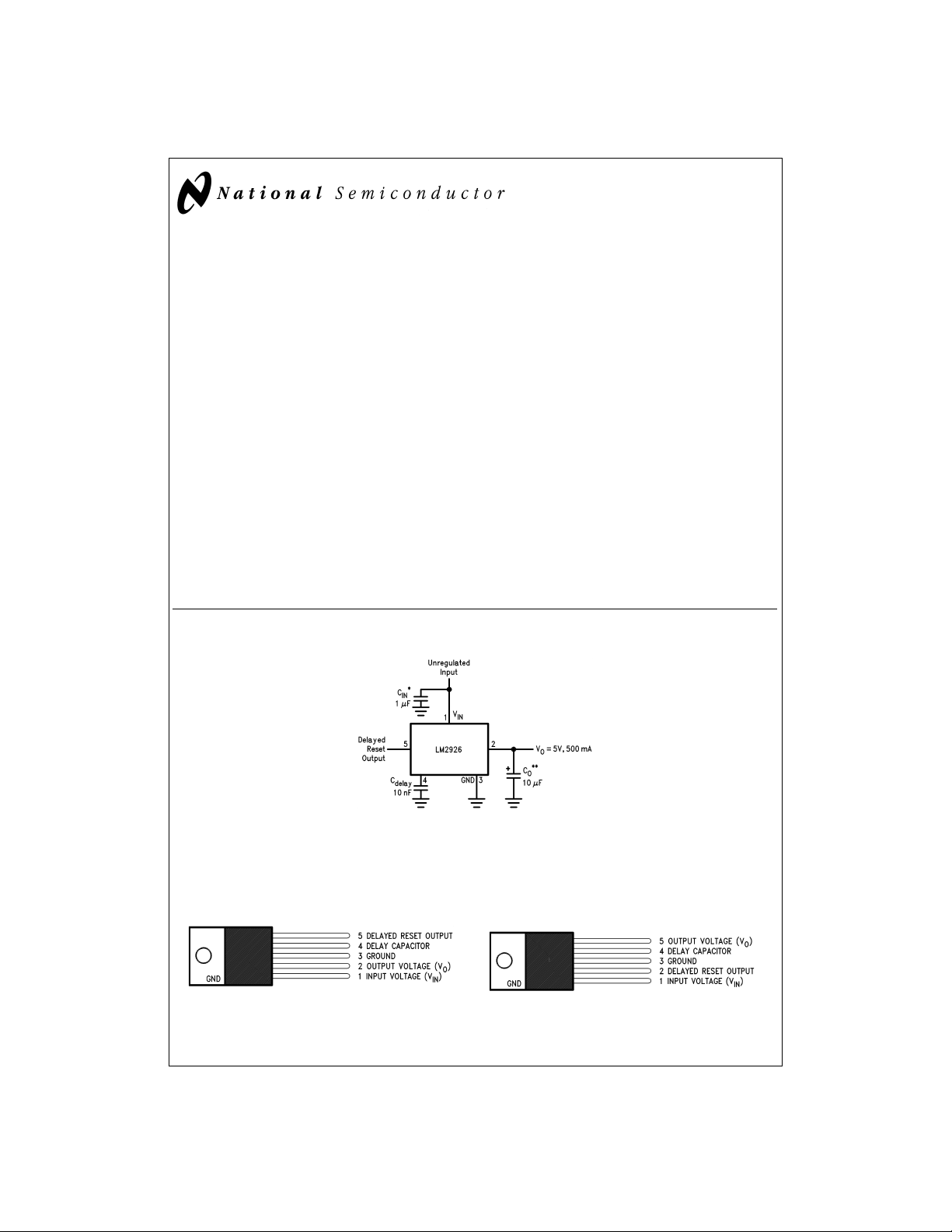
Typical Application
Features
n 5%output accuracy over entire operating range
n Dropout voltage typically 350 mV at 500 mA output
n Externally programmed reset delay
n Short circuit proof
n Reverse battery proof
n Thermally protected
n LM2926 is pin-for-pin compatible with the LM2925
+
n P
Product Enhancement tested
Applications
n Battery operated equipment
n Microprocessor-based systems
n Portable instruments
*
Required if regulator is located far (>2") from power supply filter.
must be at least 10 µF to maintain stability. May be increased without bound to maintain regulation during transients. Locate as close as possible to
**C
O
the regulator. This capacitor msut be rated over the same operating temperature range as the regulator. The equivalent series resistance (ESR) of this
capacitor is critical; see curve under Typical Performance Characteristics.
DS010759-1
Connection Diagrams and Ordering Information
5–Lead TO-220
DS010759-2
Front View
Order Number LM2926T
See NS Package Number TO5A
© 1998 National Semiconductor Corporation DS010759 www.national.com
5-Lead TO-220
DS010759-14
Front View
Order Number LM2927T
See NS Package Number TO5A
Page 2
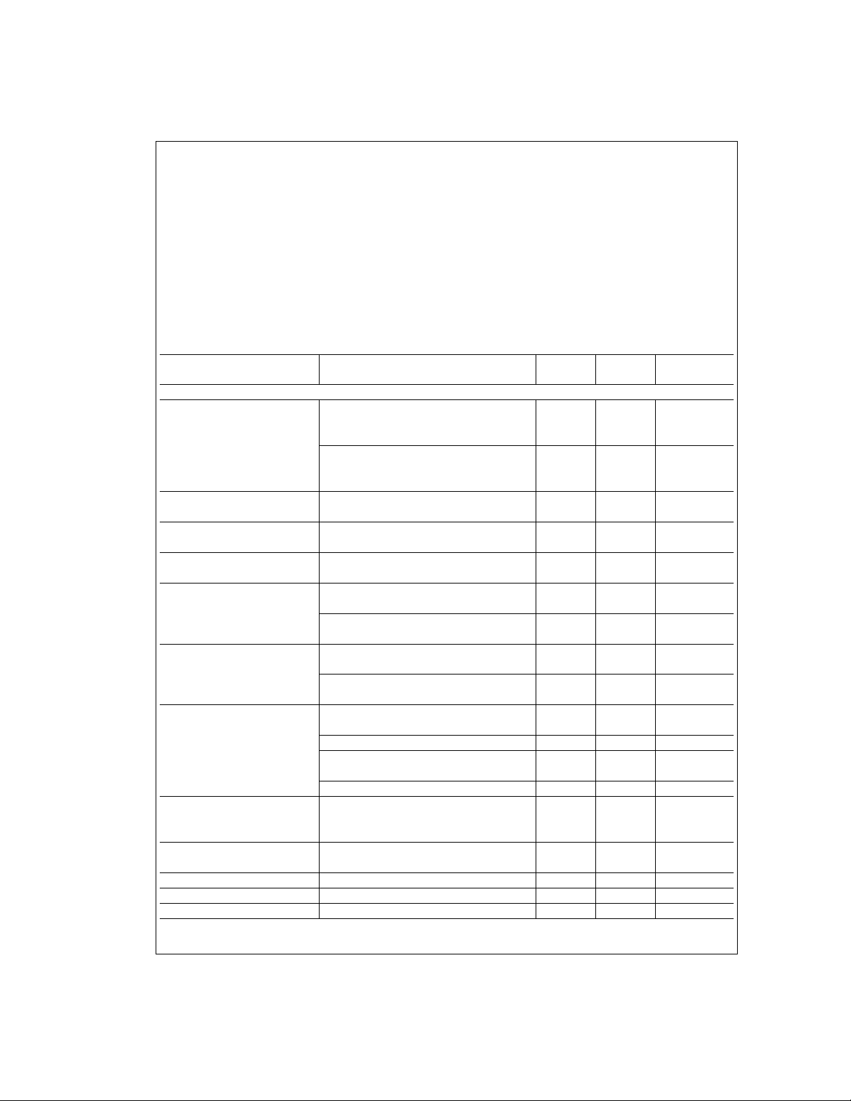
Absolute Maximum Ratings (Note 1)
If Military/Aerospace specified devices are required,
please contact the National Semiconductor Sales Office/
Distributors for availability and specifications.
Input Voltage
Survival
t=100 ms 80V
t=1 ms −50V
Continuous −18V to +26V
Power Dissipation (Note 3) Internally Limited
Junction Temperature (T
) 150˚C
JMAX
Storage Temperature Range −40˚C to +150˚C
Lead Temperature
(Soldering, 10 sec.) 260˚C
Operating Ratings(Note 1)
Junction Temperature Range (T
Maximum Input Voltage 26V
) −40˚C to +125˚C
J
Reset Output Sink Current 10 mA
ESD Susceptibility (Note 2) 2 kV
Electrical Characteristics
=
V
14.4V, C
IN
REGULATOR OUTPUT
Output Voltage 5 mA ≤ I
Line Regulation I
Load Regulation 5 mA ≤ I
Quiescent Current I
Quiescent Current at Low V
Dropout Voltage (Note 6) I
Short Circuit Current V
Ripple Rejection ƒ
Output Impedance I
Output Noise 10 Hz to 100 kHz, I
Long Term Stability 20 mV/1000 Hr
=
10 µF, −40˚C ≤ T
O
≤ 125˚C, unless otherwise specified.
J
Parameter Conditions Typ Limit Units
(Note 4) (Note 5) (Limit)
≤ 500 mA, 4.85 V (min)
O
=
T
25˚C 5 V
J
5.15 V (max)
5mA≤I
≤500 mA 4.75 V (min)
O
5V
5.25 V (max)
=
5 mA, 9V ≤ V
O
≤ 16V 1 mV
IN
25 mV (max)
=
I
5 mA, 7V ≤ V
O
≤ 26V 3 mV
IN
50 mV (max)
≤ 500 mA 5 mV
O
60 mV (max)
=
5mA 2 mA
O
3 mA (max)
=
I
500 mA 8 mA
O
30 mA (max)
=
I
IN
O
5 mA, V
=
5V 3 mA
IN
10 mA (max)
=
I
O
500 mA, V
=
6V 25 mA
IN
60 mA (max)
O
=
5 mA, T
=
25˚C 60 mV
J
200 mV (max)
=
I
5 mA 300 mV (max)
O
=
I
O
500 mA, T
=
25˚C 350 mV
J
600 mV (max)
=
I
500 mA 700 mV (max)
O
=
IN
=
8V, R
1Ω 800 mA (min)
L
2A
3 A (max)
=
120 Hz, V
RIPPLE
=
I
50 mA
O
=
50 mAdc and 10 mArms
O
=
1 Vrms, 60 dB (min)
RIPPLE
@
1 kHz 100 mΩ
=
50 mA 1 mVrms
O
www.national.com 2
Page 3
Electrical Characteristics (Continued)
=
V
14.4V, C
IN
REGULATOR OUTPUT
Maximum Operational Input
Voltage
Peak Transient Input Voltage V
Reverse DC Input Voltage V
Reverse Transient Input Voltage t
RESET OUTPUT
Threshold ∆V
Output Low Voltage I
Internal Pull-Up Resistance 30 kΩ
Delay Time C
Minimum Operational V
on Power Up I
Minimum Operational V
on Power Down I
DELAY CAPACITOR PIN
Threshold Difference (∆V
Charging Current (I
Note 1: Absolute Maximum Ratings indicate limits beyond which damage to the device may occur. Operating Ratings indicate conditions for which the device is intended to be functional, but do not guarantee specific performance limits. For guaranteed specifications and test conditions, see the Electrical Characteristics.
Note 2: Human body model; 100 pF discharged through a 1.5 kΩ resistor.
Note 3: The maximum power dissipation is a function of T
any ambient temperature is P
down. For the LM2926 and LM2927, the junction-to-ambient thermal resistance is 53˚C/W, and the junction-to-case thermal resistance is 3˚C/W.
Note 4: Typicals are at T
Note 5: Limits are 100%guaranteed by production testing.
Note 6: Dropout voltage is the input-output differential at which the circuit ceases to regulate against any further reduction in input voltage. Dropout voltage is mea-
sured when the output voltage (V
Note 7: The reset flag is set LOW when the output voltage has dropped an amount, ∆V
=
10 µF, −40˚C ≤ T
O
≤ 125˚C, unless otherwise specified.
J
Parameter Conditions Typ Limit Units
(Note 4) (Note 5) (Limit)
Continuous 26 V (min)
O
O
r
L
≥ −0.6V, R
=
1 ms, R
O
=
L
Required for Reset Condition (Note 7) −80 mV (min)
=
≤ 7V, R
=
100Ω,t
=
L
100 ms 80 V (min)
f
100Ω −18 V (min)
100Ω −50 V (min)
−250 mV
−400 mV (max)
SINK
=
1.6 mA, V
=
3.2V 0.15
IN
0.4 V (max)
=
10 nF (See Timing Curve) 19 ms
DELAY
IN
O
DELAY
Delayed Reset Output ≤ 0.8V, 2.2 V
SINK
=
1.6 mA, R
=
100Ω 3.2 V (min)
L
Delay Reset Output ≤ 0.8V, 0.7 V
SINK
=
10 µA, V
=
0V
IN
) Change in Delay Capacitor Voltage Required 3.5 V (min)
for Reset Output to Return High 3.75 V
4.1 V (max)
) 1.0 µA (min)
DELAY
2.0 µA
3.0 µA (max)
, and θJA, and TA, and is limited by thermal shutdown. The maximum allowable power dissipation at
=
D
=
25˚C and represent the most likely parametric norm.
J
)/θJA. If this dissipation is exceeded, the die temperature will rise above 150˚C and the device will go into thermal shut-
(T
JMAX–TA
) has dropped 100 mV from the nominal value measured at V
O
JMAX
=
14.4V.
IN
, from the nominal value measured at V
O
=
14.4V.
IN
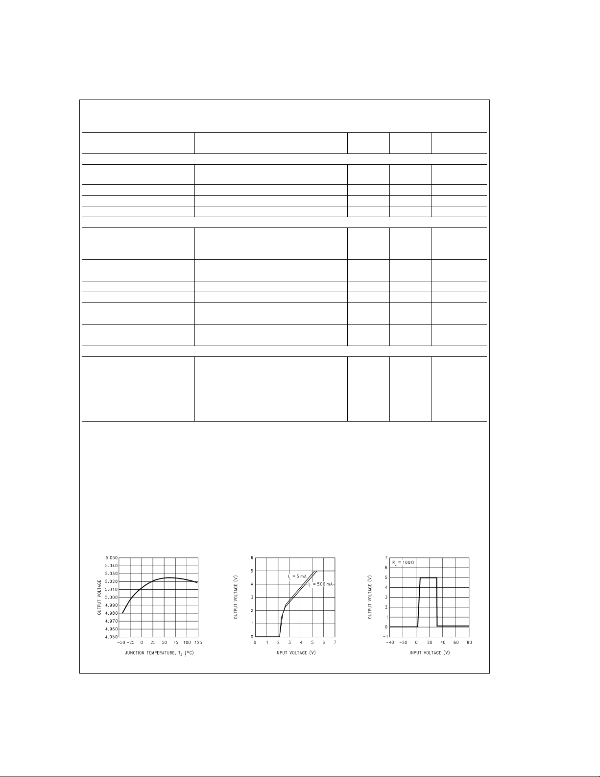
Typical Performance Characteristics
Output Voltage
DS010759-15
Low Voltage Behavior
Output at Voltage Extremes
DS010759-16
3 www.national.com
DS010759-32
Page 4

Typical Performance Characteristics (Continued)
Supply Current
Dropout Voltage
Ripple Rejection
DS010759-17
DS010759-20
Quiescent Current
Output Current Limit
Ripple Rejection
DS010759-18
DS010759-21
Quiescent Current
DS010759-19
Output Capacitor ESR
DS010759-22
Output Impedance
DS010759-23
Line Transient Response
DS010759-26
Load Transient Response
www.national.com 4
DS010759-24
DS010759-27
DS010759-25
Maximum Power
Dissipation (TO-220)
DS010759-28
Page 5

Typical Performance Characteristics (Continued)
Reset Delay
DS010759-29
Typical Circuit Waveforms
Reset Delay
DS010759-30
Applications Information
EXTERNAL CAPACITORS
The LM2926/7 output capacitor is required for stability. Without it, the regulator output will oscillate at amplitudes as high
as several volts peak-to-peak at frequencies up to 500 kHz.
Although 10 µF is the minimum recommended value, the actual size and type may vary depending upon the application
load and temperature range. Capacitor equivalent series resistance (ESR) also affects stability. The region of stable operation is shown in the Typical Performance Characteris-
tics (Output Capacitor ESR curve).
Output capacitors can be increased in size to any desired
value above 10 µF.One possible purpose of this would be to
maintain the output voltage during brief conditions of input
transients that might be characteristic of a particular system.
Capacitors must also be rated at all ambient temperatures
expected in the system. Many aluminum electrolytics freeze
at temperatures below −30˚C, reducing their effective capacitance to zero. To maintain regulator stability down to
−40˚C, capacitors rated at that temperature (such as tantalums) must be used.
DS010759-5
DELAYED RESET
The delayed reset output is designed to hold a microprocessor in a reset state on system power-up for a programmable
time interval to allow the system clock and other powered circuitry to stabilize.A full reset interval is also generated whenever the output voltage falls out of regulation. The circuit is
tripped whenever the output voltage of the regulator is out of
regulation by the Reset Threshold value. This can be caused
by low input voltages, over current conditions, over-voltage
shutdown, thermal shutdown, and by both power-up and
power-down sequences. When the reset circuit detects one
of these conditions, the delay capacitor is discharged by an
SCR and held in a discharged state by a saturated NPN
switch. As long as the delay capacitor is held low, the reset
output is also held low.Because of the action of the SCR, the
reset output cannot glitch on noise or transient fault conditions.A full reset pulse is obtained for any fault condition that
trips the reset circuit.
When the output regains regulation, the SCR is switched off
and a small current (I
5 www.national.com
=
2 µA) begins charging the de-
DELAY
Page 6

Applications Information (Continued)
lay capacitor. When the capacitor voltage increases 3.75V
(∆V
) from its discharged value, the reset output is
DELAY
again set HIGH. The delay time is calculated by:
The constant, 1.9 x 10⁶, has a±20%tolerance from device
to device. The total delay time error budget is the sum of the
20%device tolerance and the tolerance of the external capacitor.For a 20%timing capacitor tolerance, the worst case
total timing variation would amount to
2.33:1. In most applications the minimum expected reset
pulse is of interest. This occurs with minimum C
mum ∆V
are fully specified in the Electrical Characteristics. Graphs
, and maximum I
DELAY
showing the relationship between delay time and both temperature and C
Characteristics.
As shown in
are shown in the Typical Performance
DELAY
Figure 1
, the delayed reset output is pulled low
by an NPN transistor (Q2), and pulled high to V
nal 30 kΩ resistor (R3) and PNP transistor (Q3). The reset
output will operate when V
more).At lower voltages the reset output will be in a high im-
is sufficient to bias Q2 (0.7V or
O
pedance condition. Because of differences in the V
and Q3 and the values of R1 and R2, Q2 is guaranteed by
design to bias
the high impedance state when V
state when V
before
Q3, providing a smooth transition from
>
0.7V.
O
±
40%, or a ratio of
. ∆V
DELAY
DELAY
<
0.7V,to the active low
O
DELAY
and I
by an inter-
O
BE
, mini-
DELAY
of Q2
DS010759-7
FIGURE 2. Reset Output Behavior during Power-Up
Figure 2
is useful for determing reset performance at any
particular input voltage. Dynamic performance at power-up
will closely follow the characteristics illustrated in
except for the delay added by C
when VOreaches 5V.
DELAY
Figure 2
The dynamic reset characteristics at power-down are illustrated by the curve shown in
Figure 3
. At time t=0 the input
voltage is instantaneously brought to 0V, leaving the output
powered by C
a 100Ω load resistor), the reset output is held low. As V
.As the voltage on COdecays (discharged by
O
drops below 0.7V, the reset rises up slightly should there be
any external pull-up resistance. With no external resistance,
the reset line stays low throughout the entire power down
cycle. If the input voltage does not fall instantaneously, the
reset signal will tend to follow the performance characteristics shown in
Figure 2
.
SYSTEM DESIGN CONSIDERATIONS
Many microprocessors are specified for operation at 5V
±
10%, although they often continue operating well outside
this range. Others, such as certain members of the COPS
family of microcontrollers, are specified for operation as low
as 2.4V.
,
O
DS010759-6
FIGURE 1. Delay Reset Output
Figure 2
The static reset characteristics are shown in
. This
shows the relationship between the input voltage, the regultor output and reset output. Plots are shown for various external pull-up resistors ranging in value from 3 kΩ to an open
circuit. Any external pull-up resistance causes the reset output to follow the regulator output until Q2 is biased ON. C
has no effect on this characteristic.
LAY
www.national.com 6
-
DE
DS010759-8
FIGURE 3. Reset Output Behavior during Power-Down
Of particular concern is low voltage operation, which occurs
in battery operated systems when the battery reaches the
end of its discharge cycle. Under this condition, when the
supply voltage is outside the guaranteed operating range,
the clock may continue to run and the microprocessor will attempt to execute instructions. If the supply voltage is outside
the guaranteed operating range, the instructions may not execute properly and a hardware reset such as is supplied by
Page 7

Applications Information (Continued)
the LM 2926/7 may fail to bring the processor under control.
The LM2926/7 reset output may be more efficiently employed in certain applications as a means of defeating
memory WRITE lines, clocks, or external loads, rather than
depending on unspecified microprocessor operating conditions.
In critical applications the microprocessor reset input should
be fully characterized and guaranteed to operate until the
clock ceases oscillating.
INPUT TRANSIENTS
The LM2926/7 are guaranteed to withstand positive input
transients to 80V followed by an exponential decay of
τ=20 ms (t
ing an output of less than 7V. The regulator remains operational to 26 V
=
100 ms, or 5 time constants) while maintain-
f
, and shuts down if this value is exceeded.
DC
Typical Applications
Battery Powered Regulator with Flashing
LED for Low Battery Indication
DS010759-9
General Microprocessor Configuration
DS010759-10
7 www.national.com
Page 8

Typical Applications (Continued)
Using the Reset to De-Activate Power Loads. The LM1921 is a Fully Protected 1 Amp High-Side Driver.
DS010759-11
Generating an Active High Reset Signal
Using the Reset to Ensure an Accurate Display
on Power-Up or Power-Down
www.national.com 8
DS010759-12
DS010759-13
Page 9

9
Page 10

Physical Dimensions inches (millimeters) unless otherwise noted
5-Lead TO-220 Outline Drawing
Order Number LM2926T or LM2927T
NS Package Number T05A
LM2926/LM2927 Low Dropout Regulator with Delayed Reset
LIFE SUPPORT POLICY
NATIONAL’S PRODUCTS ARE NOT AUTHORIZED FOR USE AS CRITICAL COMPONENTS IN LIFE SUPPORT DEVICES OR SYSTEMS WITHOUT THE EXPRESS WRITTEN APPROVAL OF THE PRESIDENT OF NATIONAL SEMICONDUCTOR CORPORATION. As used herein:
1. Life support devices or systems are devices or sys-
tems which, (a) are intended for surgical implant into
the body, or (b) support or sustain life, and whose failure to perform when properly used in accordance
with instructions for use provided in the labeling, can
be reasonably expected to result in a significant injury
to the user.
National Semiconductor
Corporation
Americas
Tel: 1-800-272-9959
Fax: 1-800-737-7018
Email: support@nsc.com
www.national.com
National does not assume any responsibility for use of any circuitry described, no circuit patent licenses are implied and National reserves the right at any time without notice to change said circuitry and specifications.
National Semiconductor
Europe
Fax: +49 (0) 1 80-530 85 86
Email: europe.support@nsc.com
Deutsch Tel: +49 (0) 1 80-530 85 85
English Tel: +49 (0) 1 80-532 78 32
Français Tel: +49 (0) 1 80-532 93 58
Italiano Tel: +49 (0) 1 80-534 16 80
2. A critical component in any component of a life support
device or system whose failure to perform can be reasonably expected to cause the failure of the life support
device or system, or to affect its safety or effectiveness.
National Semiconductor
Asia Pacific Customer
Response Group
Tel: 65-2544466
Fax: 65-2504466
Email: sea.support@nsc.com
National Semiconductor
Japan Ltd.
Tel: 81-3-5620-6175
Fax: 81-3-5620-6179
 Loading...