

Page 1
现货库存、技术资料、百科信息、热点资讯,精彩尽在鼎好!
LM2904,LM358/LM358A,LM258/
LM258A
Dual Operational Amplifier
www.fairchildsemi.com
Features
• Internally Frequency Compensated for Unity Gain
• Large DC Voltage Gain: 100dB
• Wide Power Supply Range:
LM258/LM258A, LM358/LM358A: 3V~32V (or ±1.5V
~ 16V)
LM2904 : 3V~26V (or ±1.5V ~ 13V)
• Input Common Mode Voltage Range Includes Ground
• Large Output Voltage Swing: 0V DC to Vcc -1.5V DC
• Power Drain Suitable for Battery Operation.
Description
The LM2904,LM358/LM358A, LM258/LM258A consist of
two independent, high gain, internally frequency
compensated operational amplifiers which were designed
specifically to operate from a single power supply over a
wide range of voltage. Operation from sp lit power supplies
is also possible and the low power supply cu rrent drain is
independent of the magnitude of the power supply voltage.
Application areas include transducer amplifier, DC gain
blocks and all the conventional OP-AMP circuits which now
can be easily implemented in single power supply systems.
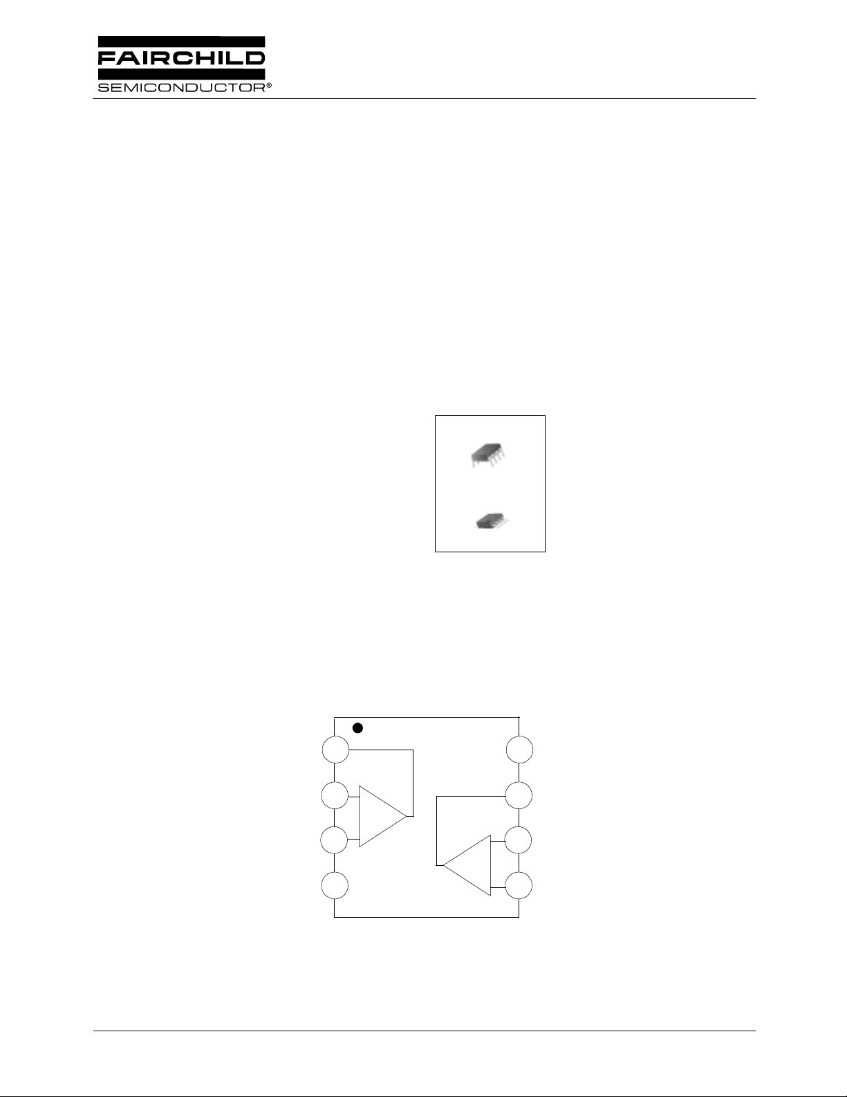
8-DIP
1
8-SOP
1
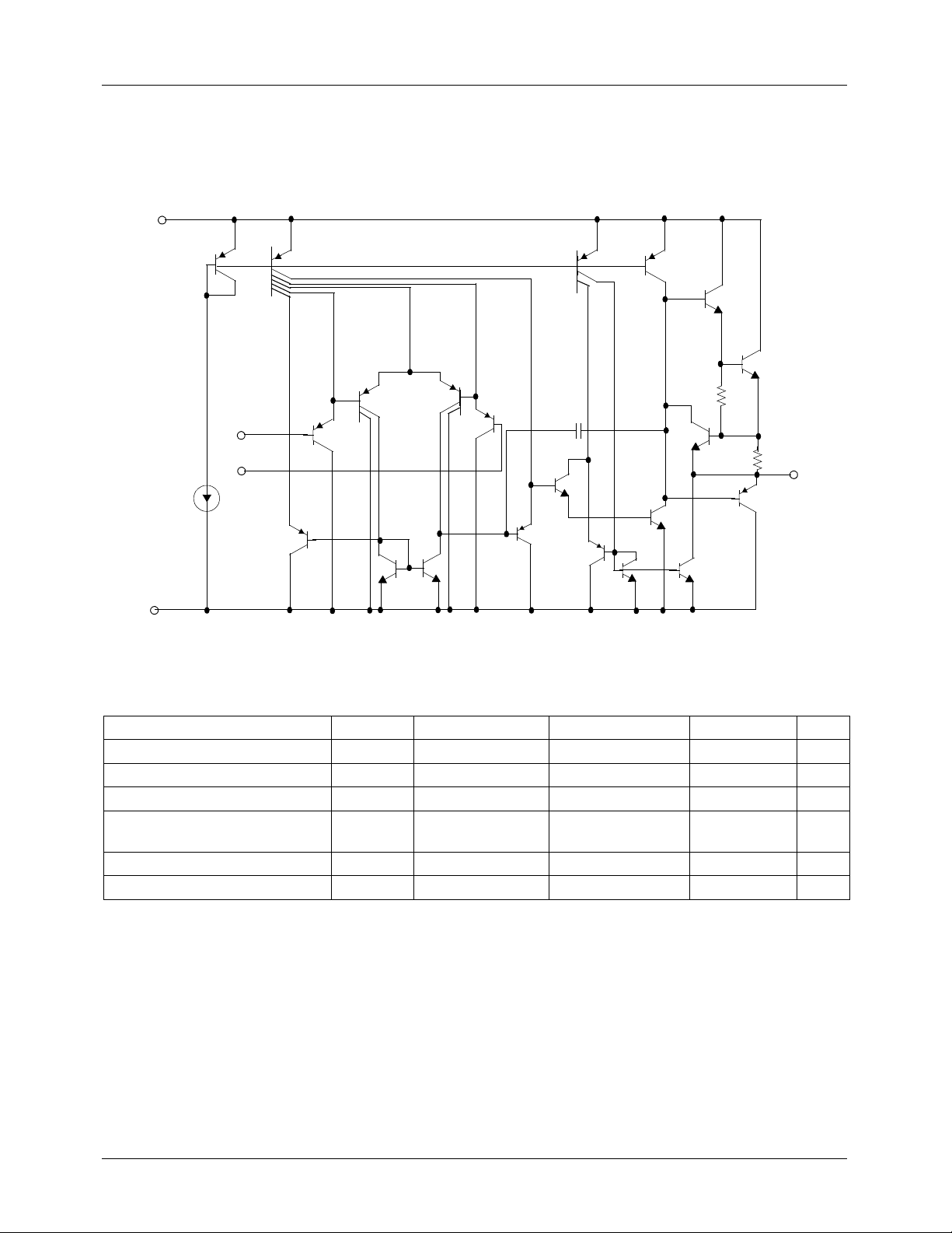
Internal Block Diagram
OUT1
IN1 (-)
IN1 (+)
GND
©2002 Fairchild Semiconductor Corporation
1
2
-
+
3
45
-
+
8
7
6
V
CC
OUT2
IN2 (-)
IN2 (+)
Rev. 1.0.2
Page 2
LM2904,LM358/LM358A,LM258/LM258A
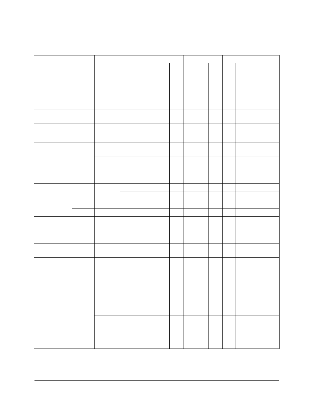
Schematic Diagram
(One section only)
V
CC
IN(-)
IN(+)
Q6
Q1
Q7
Q5
GND
Absolute Maximum Ratings
Q2
Q8
Q9
Q3
Q4
Q10
Q11
C1
Q13
Q12
Q14
Q17
Q15
Q18
Q16
Q19
R1
Q20
Q21
R2
OUTPUT
Parameter Symbol LM258/LM258A LM358/LM358A LM2904 Unit
Supply Voltage V
Differential Input Voltage V
I(DIFF)
Input Voltage V
Output Short Circuit to GND
V
≤15V, T
CC
Operating Temperature Range T
Storage Temperature Range T
= 25°C(One Amp)
A
OPR
STG
CC
I
- Continuous Continuous Continuous -
±16 or 32 ±16 or 32 ±13 or 26 V
32 32 26 V
-0.3 to +32 -0.3 to +32 -0.3 to +26 V
-25 ~ +85 0 ~ +70 -40 ~ +85 °C
-65 ~ +150 -65 ~ +150 -65 ~ +150 °C
2
Page 3
Electrical Characteristics
(Vcc = 5.0V, VEE = GND, TA = 25°C, unless otherwise specified)
LM2904,LM358/LM358A,LM258/LM258A
Parameter Symbol Conditions
VCM = 0V to V
Input Offset
Voltage
Input Offset
Current
Input Bias
Current
Input Voltage
Range
V
I
IO
I
BIAS
V
I(R)
IO
-1.5V
V
= 1.4V,
O(P)
R
= 0Ω
S
VCC = 30V
(LM2904, V
--330-550-550nA
- - 45 150 - 45 250 - 45 250 nA
CC
RL = ∞, VCC = 30V
Supply Current I
Large Signal
Voltage Gain
Output Voltage
Swing
Common-Mode
Rejection Ratio
Power Supply
Rejection Ratio
CMRR - 70 85 - 65 80 - 50 80 - dB
PSRR - 65 100 - 65 100 - 50 100 - dB
Channel
Separation
Short Circuit to
GND
I
SOURCE
Output Current
Differential
Input Voltage
V
CC
G
V
V
O(H)
V
O(L)
CS
I
SC
I
SINK
I(DIFF)
(LM2904, V
R
= ∞, VCC = 5V - 0.5 1.2 - 0.5 1.2 - 0.5 1.2 mA
L
VCC = 15V,
R
= 2kΩ
L
V
O(P)
VCC=30V
(V
CC
=26V for
LM2904)
VCC = 5V, R
f = 1kHz to 20kHz
(Note1)
V
I(+)
V
= 0V
I(-)
V
= 15V,
CC
V
O(P)
V
I(+)
V
= 15V,
CC
V
O(P)
V
I(+)
V
CC
V
O(P)
CC
= 1V to 11V
R
L
R
L
10kΩ
= 10kΩ - 5 20 - 5 20 - 5 20 mV
L
- - 40 60 - 40 60 - 40 60 mA
= 1V,
= 2V
= 0V, V
I(-)
= 2V
= 0V,V
I(-)
= 15V,
= 200mV
---V
LM258 LM358 LM2904
Min. Typ. Max. Min. Typ. Max. Min. Typ. Max.
CC
Unit
- 2.9 5.0 - 2.9 7.0 - 2.9 7.0 mV
=26V)
=26V)
Vcc
-1.5 0 -
0-
Vcc
-1.5
0-
- 0.8 2.0 - 0.8 2.0 - 0.8 2.0 mA
Vcc
-1.5 V
50 100 - 25 100 - 25 100 - V/mV
= 2kΩ 26 - - 26 - - 22 - - V
=
27 28 - 27 28 - 23 24 - V
- 120 - - 120 - - 120 - dB
20 30 - 20 30 - 20 30 - mA
= 1V,
10 15 - 10 15 - 10 15 - mA
=1V ,
12 100 - 12 100 - - - - µA
--VCC--VCCV
CC
Note:
1. This parameter, although guaranteed, is not 100% tested in production.
3
Page 4
LM2904,LM358/LM358A,LM258/LM258A
Electrical Characteristics
(VCC= 5.0V, V
The following specification apply over the range of -25°C ≤ T
for the LM358; and the -40°C ≤ T
Parameter Symbol Conditions
= GND, unless otherwise specified)
EE
(Continued)
≤ +85°C for the LM2904
A
Min. Typ. Max. Min. Typ. Max. Min. Typ. Max.
VCM = 0V to
V
Input Offset
Voltage
Input Offset
Voltage Drift
Input Offset
Current
Input Offset
Current Drift
Input Bias
Current
Input Voltage
Range
Large Signal
Voltage Gain
Output Voltage
Swing
Output Current
Differential
Input Voltage
V
IO
∆V
IO/∆T
I
IO
∆I
/∆T - -10 - -10- -10-pA/°C
IO
I
BIAS
V
I(R)
G
V
V
O(H)
V
O(L)
I
SOURCE
I
SINK
V
I(DIFF)
-1.5V
CC
V
= 1.4V,
O(P)
R
= 0Ω
S
RS = 0Ω
- - - 100 - - 150 - 45 200 nA
- - 40 300 - 40 500 - 40 500 nA
VCC = 30V
(LM2904 ,
V
= 26V)
CC
VCC = 15V,
=2.0kΩ
R
L
V
= 1V to 11V
O(P)
VCC=30V
(V
=
CC
26V for
LM2904)
VCC = 5V, R
V
= 1V,
I(+)
V
= 0V
I(-)
V
= 15V,
CC
V
= 2V
O(P)
V
= 0V,
I(+)
V
= 1V
I(-)
V
= 15V,
CC
V
= 2V
O(P)
---V
- - 7.0 - - 9.0 - - 10.0 mV
- 7.0 - - 7.0 - - 7.0 - µV/°C
0-
25 - - 15 - - 15 - - V/mV
RL = 2kΩ 26 - - 26 - - 22 - - V
=10kΩ 27 28 - 27 28 - 23 24 - V
R
L
=10kΩ
L
- 5 20 - 5 20 - 5 20 mV
10 30 - 10 30 - 10 30 - mA
58 - 59 - 59 -mA
≤ +85°C for the LM258; and the 0°C ≤ TA ≤ +70°C
A
LM258 LM358 LM2904
Vcc
-2.0
CC
Vcc
0-
--VCC--VCCV
-2.0 0 -
Vcc
-2.0 V
Unit
4
Page 5

LM2904,LM358/LM358A,LM258/LM258A
Electrical Characteristics
(VCC = 5.0V, V
Parameter Symbol Conditions
Input Offset Voltage V
Input Offset Current I
Input Bias Current I
Input Voltage Range V
Supply Current I
Large Signal Voltage
Gain
Output Voltage Swing
Common-Mode
Rejection Ratio
Power Supply
Rejection Ratio
= GND, TA = 25°C, unless otherwise specified)
EE
IO
IO
BIAS
I(R)
CC
G
V
V
OH
V
O(L)
CMRR - 70 85 - 65 85 - dB
PSRR - 65 100 - 65 100 - dB
(Continued)
LM258A LM358A
Min. Typ. Max. Min. Typ. Max.
VCM = 0V to VCC -1.5V
V
= 1.4V, RS = 0Ω
O(P)
- 1.0 3.0 - 2.0 3.0 mV
- -215-530nA
- - 40 80 - 45 100 nA
VCC = 30V 0 -
V
CC
-1.5
0-
V
CC
-1.5
RL = ∞,VCC = 30V - 0.8 2.0 - 0.8 2.0 mA
RL = ∞, V
VCC = 15V, R
= 1V to 11V
V
O
VCC = 30V
VCC = 5V, R
= 5V - 0.5 1.2 - 0.5 1.2 mA
CC
= 2kΩ
L
R
= 2kΩ 26 - - 26 - - V
L
R
=10kΩ 27 28 - 27 28 - V
L
=10kΩ - 5 20 - 5 20 mV
L
50 100 - 25 100 - V/mV
Channel Separation CS f = 1kHz to 20kHz (Note1) - 120 - - 120 - dB
Short Circuit to GND I
I
SOURCE
Output Current
Differential Input
Voltage
V
SC
I
SINK
I(DIFF)
V
V
V
V
V
V
I(+)
CC
I(+)
CC
in +
O(P)
= 1V, V
= 15V, V
= 1V, V
= 15V, V
= 0V, V
- - 40 60 - 40 60 mA
= 0V
I(-)
= 2V
O(P)
= 0V
I(-)
= 2V
O(P)
= 1V
in (-)
= 200mV
---V
20 30 - 20 30 - mA
10 15 - 10 15 - mA
12 100 - 12 100 - µA
--VCCV
CC
Unit
V
Note:
1. This parameter, although guaranteed, is not 100% tested in production.
5
Page 6

LM2904,LM358/LM358A,LM258/LM258A
Electrical Characteristics
(VCC = 5.0V, V
= GND, unless otherwise specified)
EE
(Continued)
The following specification apply over the range of -25°C ≤ T
for the LM358A
Parameter Symbol Conditions
Input Offset Voltage V
Input Offset Voltage Drift ∆V
Input Offset Current I
Input Offset Current Drift ∆I
Input Bias Current I
Input Common-Mode
Voltage Range
Output Voltage Swing
IO
BIAS
V
V
V
Large Signal Voltage Gain G
I
SOURCE
Output Current
I
SINK
Differential Input Voltage V
I(DIFF)
IO
IO
IO
I(R)
O(H)
O(L)
V
VCM = 0V to VCC -1.5V
V
= 1.4V, RS = 0Ω
O(P)
/∆T - -7.015 -7.020µV/°C
- --30--75nA
/∆T - - 10 200 - 10 300 pA/°C
- - 40 100 - 40 200 nA
VCC = 30V 0 -
R
VCC = 30V
L
R
L
VCC = 5V, RL=10kΩ -520-520mV
VCC = 15V, RL=2.0kΩ
= 1V to 11V
V
O(P)
V
I(+)
V
CC
V
I(+)
V
CC
= 1V, V
= 15V, V
= 1V, V
= 15V, V
I(-)
O(P)
I(-)
O(P)
= 0V
= 0V
---V
≤ +85°C for the LM258A; and the 0°C ≤ TA ≤ +70°C
A
LM258A LM358A
Min. Typ. Max. Min. Typ. Max.
Unit
--4.0--5.0mV
Vcc
-2.0
0-
Vcc
-2.0
= 2kΩ 26 - - 26 - - V
= 10kΩ 27 28 - 27 28 - V
25 - - 15 - - V/mV
= 2V
= 2V
10 30 - 10 30 - mA
59 - 59 - mA
--VCCV
CC
V
6
Page 7

Typical Performance Characteristics
Figure 1. Supply Current vs Supply Voltage Figure 2. Voltage Gain vs Supply Voltage
LM2904,LM358/LM358A,LM258/LM258A
Figure 3. Open Lo op Frequency R esponse Figure 4. Large Signal Output Swing vs Fr equency
Figure 5. Output Characteristics vs Current Sourcing Figure 6. Output Characteristics vs Current Sinking
7
Page 8

LM2904,LM358/LM358A,LM258/LM258A
Typical Performance Characteristics
Figure 7. Input Voltage Range vs Supply Voltage Figure 8. Common-Mode Rejection Ratio
(Continued)
Figure 9. Output Current vs Tempe rature (Current L im itin g) Figure 10. Input Current vs Temperature
Figure 11. Voltage Follower Pulse Response Figure 12. Voltage Follower Pulse Response
(Small Signal)
8
Page 9

Mechanical Dimensions
Package
6.40 ±0.20
0.252
±0.008
8-DIP
LM2904,LM358/LM358A,LM258/LM258A
Dimensions in millimeters
0.79
0.031
()
±0.10
#1
#4 #5
7.62
0.300
#8
MAX
9.20 ±0.20
9.60
0.378
5.08
MAX
0.200
3.40 ±0.20
0.134 ±0.008
0.362 ±0.008
0.33
0.013
3.30 ±0.30
0.130 ±0.012
MIN
0.46
2.54
0.018 ±0.004
0.100
1.524 ±0.10
0.060 ±0.004
0~15°
0.25
0.010
+0.10
–0.05
+0.004
–0.002
9
Page 10

LM2904,LM358/LM358A,LM258/LM258A
Mechanical Dimensions
Package
#1
#4
(Continued)
8-SOP
1.55 ±0.20
0.061 ±0.008
#8
#5
MAX
5.13
0.202
Dimensions in millimeters
0.1~0.25
MIN
0.004~0.001
0.56
0.022
()
4.92 ±0.20
0.194 ±0.008
0.006
0.15
+
-0.002
-0.05
0.004
0.50 ±0.20
0.020 ±0.008
+
0.10
6.00 ±0.30
0.236 ±0.012
3.95 ±0.20
0.156 ±0.008
5.72
0.225
0.071
0~8°
1.80
MAX
MAX0.10
MAX0.004
1.27
0.050
0.41 ±0.10
0.016 ±0.004
10
Page 11

Ordering Information
Product Number Package Operating Temperature
LM358N
LM358AN
LM358M
LM358AM
LM2904N 8-DIP
LM2904M 8-SOP
LM258N
LM258AN
LM258M
LM258AM
8-DIP
0 ~ +70°C
8-SOP
-40 ~ +85°C
8-DIP
-25 ~ +85°C
8-SOP
LM2904,LM358/LM358A,LM258/LM258A
11
Page 12

LM2904,LM358/LM358A,LM258/LM258A
DISCLAIMER
FAIRCHILD SEMICONDUCTOR RESERVES THE RIGHT TO MAKE CHANGES WITHOUT FURT HER NOTICE TO ANY
PRODUCTS HEREI N TO IMPROVE RELIABILITY, FUNCTIO N OR DESIGN. FAIRCH IL D DOES NOT ASSUME ANY
LIABILITY ARISING OUT OF THE APPLICATION OR USE OF ANY PRODUCT OR CIRCUIT DESCRIBED HEREIN; NEITHER
DOES IT CONVEY ANY LICENSE UNDER IT S PATENT RIGHTS, NOR THE RIGHTS OF OTHE RS.
LIFE SUPPORT POL I CY
FAIRCHILD’S PR ODUCTS ARE NOT AUTH ORIZED FOR USE AS C RITICAL COMPONENT S IN LIFE SUPPORT DE VICES
OR SYSTEMS WITHOUT THE EXPRESS WRITTEN APPROVAL OF THE PRESIDENT OF FAIRCHILD SEMICONDUCTOR
CORPORATION. As used herein :
1. Life support devices or systems are devices or systems
which, (a) are intended for surgical implant into the body,
or (b) support or sustain life, and (c) whose failure to
perform when properly used in accordance with
2. A critical component in any component of a life support
device or sy stem whose fai lure to perform can be
reasonably expec ted to cause the failur e of the life support
device or system, or to affect its safety or effec t iv ene ss .
instructions for use provided in the labeling, can be
reasonably expected to result in a significant injury of the
user.
www.fairchildsemi.com
8/26/02 0.0m 001
2002 Fairchild Semiconductor Corporation
Stock#DSxxxxxxxx
 Loading...