

Page 1
LM2853 Evaluation Board
Introduction
The LM2853 synchronous SIMPLE SWITCHER®buck regulator is a synchronous switching regulator capable of delivering up to 3A of current into a load. The LM2853 represents
the ultimate in ease of use, as internal type-3 compensation
minimizes the necessary external components and eases
the selection of those components. The LM2853 is capable
of accepting an input voltage between 3.0V and 5.5V and
delivering an output voltage that is factory programmable
from 0.8V to 3.3V in 100mV increments. The nominal switching frequency of the LM2853 is 550 kHz.
The LM2853 Evaluation Board was designed to accommodate three standard output voltage options (1.2V/1.8V/3.3V)
using the same layout and external components. Just five
external components are included on the board, and the
entire 3A power supply occupies a minimum amount of
space (1.2” by 0.82”) on a two layer PCB without sacrificing
efficiency or performance. The input voltage can be varied
over the entire operating range of the LM2853 (3.0V to 5.5V)
for testing purposes. Also, the board is designed to be stable
with all standard LM2853 voltage options, so if another
voltage option needs to be tested, the LM2853 IC can be
removed and replaced with the desired option.
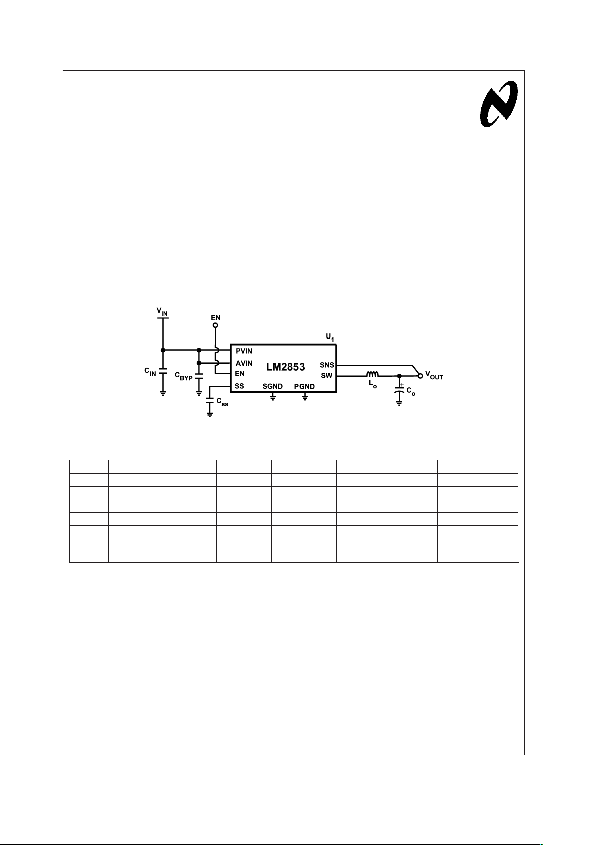
Schematic
20201803
Bill Of Material
ID Part Number Type Size Parameters QTY Vendor
U1 LM2853MH-x.x/NOPB 3A Buck ETSSOP-14 x.xV 1 NSC
C
IN
GRM31CR60J476ME19 Capacitor 1206 47 µF 1 Murata
C
BYP
GRM21BR71C105KA01 Capacitor 0805 1 µF 1 Murata
C
SS
VJ0805Y222KXXA Capacitor 0603 2.2 nF 1 Vishay-Vitramon
L
O
DO3316P-472 Inductor DO3316P 4.7 µH 1 Coilcraft
C
O
TPSD227X06R0050 Capacitor D Case 220 µF
(50 mΩ)
1 Vishay-Sprague
National Semiconductor
Application Note 1513
Jeff Kissinger
October 2006
LM2853 Evaluation Board AN-1513
© 2006 National Semiconductor Corporation AN202018 www.national.com
Page 2

Performance
Efficiency vs. I
LOAD(VIN
= 5V)
20201802
0.5A to 3A Load Step Response (VIN= 5V, V
OUT
= 1.8V)
20201805
Horizontal Resolution: 200 µs/Div.
Trace 1: V
OUT
(100 mV/Div.)
Trace 2: I
LOAD
(1 A /Div.)
Component Selection
CINand C
BYP
The necessary RMS current rating of the input capacitor can
be estimated by the following equation:
where the variable D refers to the duty cycle, and can be
approximated by:
From this equation, it follows that the maximum I
RMS
will
occur at a full 3A load current with the system operating at
50% duty cycle. Under this condition, the maximum I
RMS
is
given by:
Ceramic capacitors feature a very large I
RMS
rating in a small
footprint, making a ceramic capacitor ideal for this application. A 47 µF ceramic capacitor from Murata with a 4.9A I
RMS
rating provides the necessary input capacitance for the
evaluation board. For improved load regulation and transient
performance, an extra 1 µF ceramic capacitor is placed near
to the AVIN pin from V
IN
to GND. This small capacitor helps
to filter high frequency noise pulses on the supply, and
prevent those pulses from disturbing the analog control circuitry of the chip.
C
SS
The soft-start capacitor has been chosen to provide a softstart time of roughly 3 ms. Using the internal soft-start resistance of 450 kΩ and the external soft-start capacitor value of
2.2 nF, the approximate soft-start time can be calculated as
follows:
T
SS
=3xCSSxRSS=
3 x 2.2 nF x 450 kΩ = 2.97 ms ≈ 3ms
A 3 ms soft-start time will allow the LM2853 to start up
gracefully without triggering over-current protection, regardless of the operating conditions.
AN-1513
www.national.com 2
Page 3

Component Selection (Continued)
L
O
and C
O
The selection of the output filter components LOand CO, are
intrinsically linked, as both of these parameters affect the
stability of the system, and various characteristics of the
output voltage. First, a 4.7 µH inductor is chosen to allow
stable operation over the entire input voltage range (as per
the datasheet recommendations) from 3.0V to 5.5V. The size
of the inductor also directly affects the amplitude of the
inductor current ripple. This amplitude can be calculated
from the following equation:
From this, it follows that the maximum inductor current ripple
using standard operating conditions of the LM2853 and a 4.7
µH inductor will occur at V
IN
= 5.5V, and V
OUT
= 2.5V. Under
these conditions the inductor current ripple is given as:
This means an inductor must be selected with a saturation
current higher than 3.264A to ensure that the inductor will
never saturate during normal operating conditions. A Coilcraft DO3316P, 4.7 µH inductor provides the necessary current handling capabilities (I
SAT
= 5.4A) in a relatively small
footprint.
The ESR of the output capacitor affects both the ripple
voltage at the output and the overall stability of the loop. In
order to keep the output voltage ripple manageable under all
operating conditions, an ESR value of 50 mΩ is selected. As
per the datasheet recommendations, a capacitance of 220
µF will guarantee stability regardless of V
IN
and V
OUT
when
coupled with 4.7 µH inductor and 50 mΩ ESR. An AVX
low-ESR 6.3V tantalum capacitor provides the necessary
ESR and capacitance to stabilize the loop and control the
output voltage ripple, with suitable voltage derating for up to
a 3.3V output.
PCB Layout
The PCB layout of the LM2853 demo board was designed to
occupy as little board space as possible, while still following
sound layout guidelines and techniques. The input capacitor,
C
IN
is placed as close as possible to the PVIN pins and the
PGND pins, to minimize stray resistance and inductance
between C
IN
and the LM2853. Likewise, the AVIN bypass
capacitor is placed as close as possible to the AVIN and
SGND pins. PGND and SGND are connected to each other
and the ground plane at a single point, the exposed pad of
the LM2853. Also, in order to help conduct heat to the
ground plane and away from the LM2853, an array of vias is
used to connect the exposed pad to the ground plane,
instead of a single via. Finally, the sense pin trace is intentionally routed away from the SW node to minimize any EMI
pickup.
Top Layer (not to scale) Bottom Layer (not to scale)
20201804
20201801
AN-1513
www.national.com3
Page 4

Notes
THE CONTENTS OF THIS DOCUMENT ARE PROVIDED IN CONNECTION WITH NATIONAL SEMICONDUCTOR CORPORATION
(″NATIONAL″) PRODUCTS. NATIONAL MAKES NO REPRESENTATIONS OR WARRANTIES WITH RESPECT TO THE ACCURACY OR
COMPLETENESS OF THE CONTENTS OF THIS PUBLICATION AND RESERVES THE RIGHT TO MAKE CHANGES TO
SPECIFICATIONS AND PRODUCT DESCRIPTIONS AT ANY TIME WITHOUT NOTICE. NO LICENSE, WHETHER EXPRESS, IMPLIED,
ARISING BY ESTOPPEL OR OTHERWISE, TO ANY INTELLECTUAL PROPERTY RIGHTS IS GRANTED BY THIS DOCUMENT.
TESTING AND OTHER QUALITY CONTROLS ARE USED TO THE EXTENT NATIONAL DEEMS NECESSARY TO SUPPORT
NATIONAL’S PRODUCT WARRANTY. EXCEPT WHERE MANDATED BY GOVERNMENT REQUIREMENTS, TESTING OF ALL
PARAMETERS OF EACH PRODUCT IS NOT NECESSARILY PERFORMED. NATIONAL ASSUMES NO LIABILITY FOR APPLICATIONS
ASSISTANCE OR BUYER PRODUCT DESIGN. BUYERS ARE RESPONSIBLE FOR THEIR PRODUCTS AND APPLICATIONS USING
NATIONAL COMPONENTS. PRIOR TO USING OR DISTRIBUTING ANY PRODUCTS THAT INCLUDE NATIONAL COMPONENTS,
BUYERS SHOULD PROVIDE ADEQUATE DESIGN, TESTING AND OPERATING SAFEGUARDS.
EXCEPT AS PROVIDED IN NATIONAL’S TERMS AND CONDITIONS OF SALE FOR SUCH PRODUCTS, NATIONAL ASSUMES NO
LIABILITY WHATSOEVER, AND NATIONAL DISCLAIMS ANY EXPRESS OR IMPLIED WARRANTY RELATING TO THE SALE AND/OR
USE OF NATIONAL PRODUCTS INCLUDING LIABILITY OR WARRANTIES RELATING TO FITNESS FOR A PARTICULAR PURPOSE,
MERCHANTABILITY, OR INFRINGEMENT OF ANY PATENT, COPYRIGHT OR OTHER INTELLECTUAL PROPERTY RIGHT.
LIFE SUPPORT POLICY
NATIONAL’S PRODUCTS ARE NOT AUTHORIZED FOR USE AS CRITICAL COMPONENTS IN LIFE SUPPORT DEVICES OR
SYSTEMS WITHOUT THE EXPRESS PRIOR WRITTEN APPROVAL OF THE CHIEF EXECUTIVE OFFICER AND GENERAL COUNSEL
OF NATIONAL SEMICONDUCTOR CORPORATION. As used herein:
Life support devices or systems are devices which (a) are intended for surgical implant into the body, or (b) support or sustain life and whose
failure to perform when properly used in accordance with instructions for use provided in the labeling can be reasonably expected to result in
a significant injury to the user. A critical component is any component in a life support device or system whose failure to perform can be
reasonably expected to cause the failure of the life support device or system or to affect its safety or effectiveness.
National Semiconductor and the National Semiconductor logo are trademarks or registered trademarks of National Semiconductor
Corporation. All other brand or product names may be trademarks or registered trademarks of their respective holders.
Copyright © 2006 National Semiconductor Corporation.
For the most current product information visit us at www.national.com.
National Semiconductor
Americas Customer
Support Center
Email: new.feedback@nsc.com
Tel: 1-800-272-9959
National Semiconductor
Europe Customer Support Center
Fax: +49 (0) 180-530 85 86
Email: europe.support@nsc.com
Deutsch Tel: +49 (0) 69 9508 6208
English Tel: +44 (0) 870 24 0 2171
Français Tel: +33 (0) 1 41 91 8790
National Semiconductor
Asia Pacific Customer
Support Center
Email: ap.support@nsc.com
National Semiconductor
Japan Customer Support Center
Fax: 81-3-5639-7507
Email: jpn.feedback@nsc.com
Tel: 81-3-5639-7560
www.national.com
AN-1513 LM2853 Evaluation Board
 Loading...