

Page 1
LM2853
3A 550 kHz Synchronous SIMPLE SWITCHER
Regulator
®
Buck
LM2853 3A 550 kHz Synchronous SIMPLE SWITCHER
October 2006
General Description
The LM2853 synchronous SIMPLE SWITCHER®buck regulator is a 550 kHz step-down switching voltage regulator
capable of driving up to a 3A load with excellent line and load
regulation. The LM2853 accepts an input voltage between
3.0V and 5.5V and delivers a customizable output voltage
that is factory programmable from 0.8V to 3.3V in 100mV
increments. Internal type-three compensation enables a low
component count solution and greatly simplifies external
component selection. The exposed-pad TSSOP-14 package
enhances the thermal performance of the LM2853.
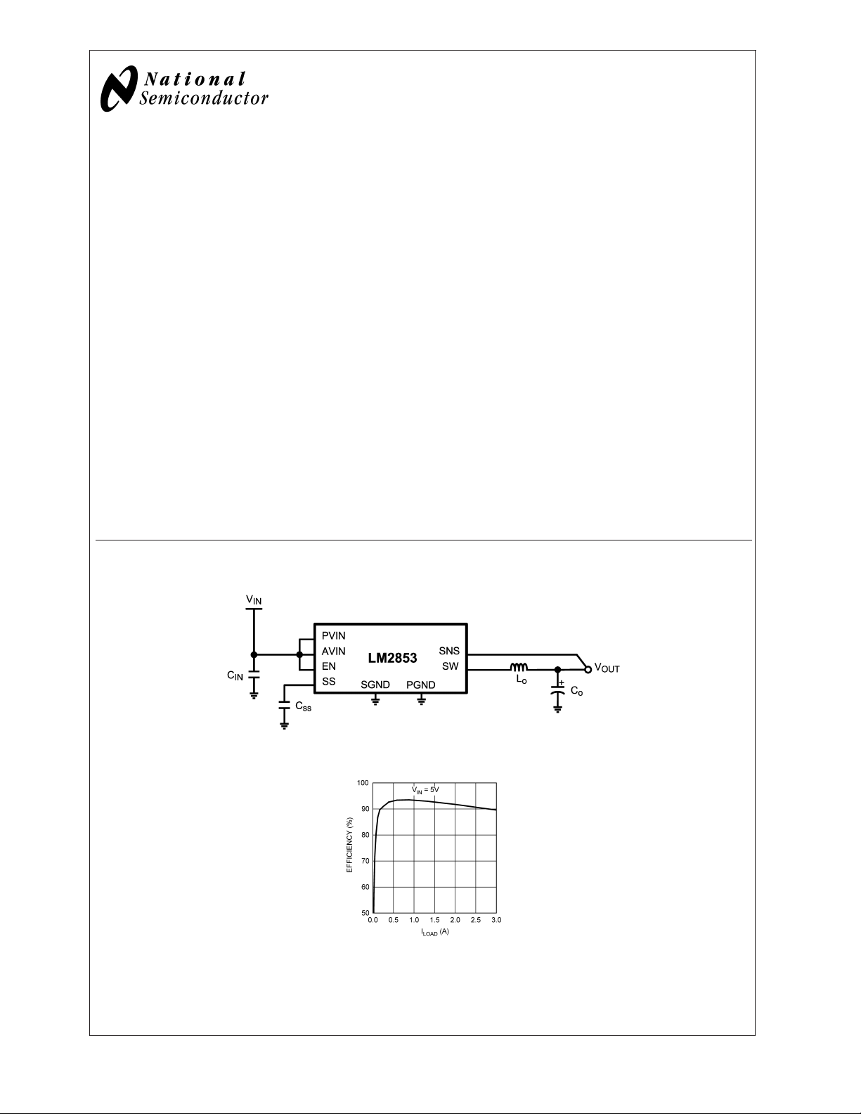
Typical Application Circuit
Features
n Input voltage range of 3.0V to 5.5V
n Factory EEPROM set output voltages from 0.8V to 3.3V
in 100 mV increments
n Maximum load current of 3A
n Voltage Mode Control
n Internal type-three compensation
n Switching frequency of 550 kHz
n Low standby current of 12 µA
n Internal 40 mΩ MOSFET switches
n Standard voltage options
0.8/1.0/1.2/1.5/1.8/2.5/3.0/3.3 volts
n Exposed pad TSSOP-14 package
Applications
n Low voltage point of load regulation
n Local solution for FPGA/DSP/ASIC core power
n Broadband networking and communications
infrastructure
®
Buck Regulator
20201502
Efficiency vs Load Current (V
SIMPLE SWITCHER®is a Registered Trademark of National Semiconductor Corporation.
© 2006 National Semiconductor Corporation DS202015 www.national.com
OUT
20201501
= 3.3V)
Page 2
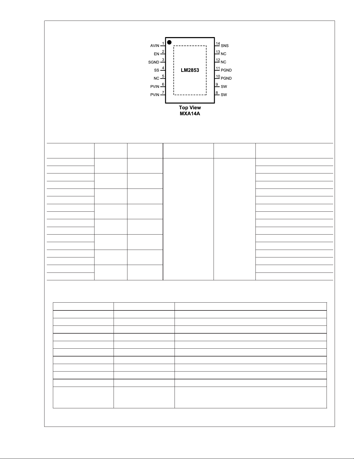
Connection Diagram
LM2853
Ordering Information
20201503
Voltage
Order Number
LM2853MH-0.8
LM2853MHX-0.8 2500 Units, Tape and Reel
LM2853MH-1.0
LM2853MHX-1.0 2500 Units, Tape and Reel
LM2853MH-1.2
LM2853MHX-1.2 2500 Units, Tape and Reel
LM2853MH-1.5
LM2853MHX-1.5 2500 Units, Tape and Reel
LM2853MH-1.8
LM2853MHX-1.8 2500 Units, Tape and Reel
LM2853MH-2.5
LM2853MHX-2.5 2500 Units, Tape and Reel
LM2853MH-3.0
LM2853MHX-3.0 2500 Units, Tape and Reel
LM2853MH-3.3
LM2853MHX-3.3 2500 Units, Tape and Reel
Note: Contact factory for other voltage options.
Option
0.8 LM2853-0.8
1.0 LM2853-1.0
1.2 LM2853-1.2
1.5 LM2853-1.5
1.8 LM2853-1.8
2.5 LM2853-2.5
3.0 LM2853-3.0
3.3 LM2853-3.3
Package
Marking Package Type
TSSOP-14 exposed
pad
Package
Drawing Supplied As
94 Units, Rail
94 Units, Rail
94 Units, Rail
94 Units, Rail
MXA14A
94 Units, Rail
94 Units, Rail
94 Units, Rail
94 Units, Rail
Pin Descriptions
Pin # Name Function
1 AVIN Input Voltage for Control Circuitry.
2 EN Enable.
3 SGND Low noise ground.
4 SS Soft-Start Pin.
5 NC No Connect. This pin must be tied to ground.
6,7 PVIN Input Voltage for Power Circuitry.
8,9 SW Switch Pin.
10,11 PGND Power Ground.
12,13 NC No-Connect. These pins must be tied to ground.
14 SNS Output Voltage Sense Pin.
Exposed Pad EP The exposed pad is internally connected to GND, but it cannot be
used as the primary GND connection. The exposed pad should be
soldered to an external GND plane.
www.national.com 2
Page 3
LM2853
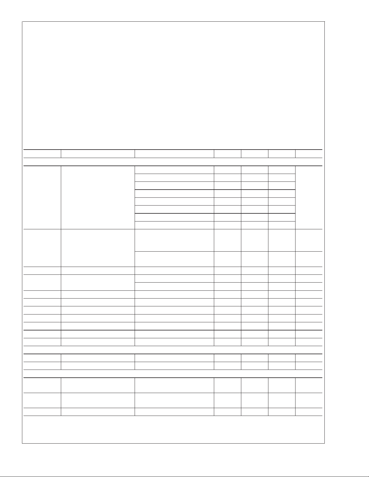
Absolute Maximum Ratings (Note 1)
If Military/Aerospace specified devices are required,
please contact the National Semiconductor Sales Office/
Distributors for availability and specifications.
14-Pin Exposed Pad TSSOP Package
Infrared (15 sec) 220˚C
Vapor Phase (60 sec) 215˚C
Soldering (10 sec) 260˚C
AVIN, PVIN, EN, SNS, SW, SS −0.3V to 6.0V
ESD Susceptibility (Note 2) 2kV
Operating Ratings (Note 1)
Power Dissipation Internally Limited
Storage Temperature Range −65˚C to +150˚C
Maximum Junction Temp. 150˚C
PVIN to GND 1.5V to 5.5V
AVIN to GND 3.0V to 5.5V
Junction Temperature −40˚C to +125˚C
Electrical Characteristics Specifications with standard typeface are for T
= 25˚C, and those in bold face
J
type apply over the full Junction Temperature Range (−40˚C to 125˚C). Minimum and Maximum limits are guaranteed through
test, design or statistical correlation. Typical values represent the most likely parametric norm at T
= 25˚C and are provided
J
for reference purposes only. Unless otherwise specified AVIN = PVIN = 5V.
Symbol Parameter Conditions Min Typ Max Units
SYSTEM PARAMETERS
V
OUT
∆V
/∆AVIN Line Regulation (Note 3) V
OUT
Voltage Tolerance (Note 3) V
= 0.8V option 0.782 0.8 0.818
OUT
V
= 1.0V option 0.9775 1.0 1.0225
OUT
V
= 1.2V option 1.1730 1.2 1.227
OUT
V
= 1.5V option 1.4663 1.5 1.5337
OUT
V
= 1.8V option 1.7595 1.8 1.8405
OUT
V
= 2.5V option 2.4437 2.5 2.5563
OUT
V
= 3.0V option 2.9325 3.0 3.0675
OUT
V
= 3.3V option 3.2257 3.3 3.3743
OUT
= 0.8V, 1.0V, 1.2V, 1.5V,
OUT
0.2 1.1 %
1.8V or 2.5V
3.0V ≤ AVIN ≤ 5.5V
= 3.0V or 3.3V
V
OUT
0.2 1.1 %
3.5V ≤ AVIN ≤ 5.5V
∆V
V
ON
OUT
/∆I
Load Regulation Normal operation 2 mV/A
O
UVLO Threshold (AVIN) Rising 2.47 3.0 V
Falling Hysteresis 50 155 260 mV
R
DS(ON)-P
R
DS(ON)-N
R
SS
I
CL
I
Q
I
SD
R
SNS
PFET On Resistance Isw = 3A 40 120 mΩ
NFET On Resistance Isw = 3A 32 100 mΩ
Soft-Start Resistance 450 kΩ
Peak Current Limit Threshold 3.6 5A
Operating Current Non-switching 0.85 2 mA
Shutdown Quiescent Current EN = 0V 12 50 µA
Sense Pin Resistance 432 kΩ
PWM
f
D
osc
range
Switching Frequency . 325 550 725 kHz
Duty Cycle Range 0 100 %
ENABLE CONTROL (Note 4)
V
IH
V
IL
I
EN
EN Pin Minimum High Input 75 %of
EN Pin Maximum Low Input 25 %of
EN Pin Pullup Current EN = 0V 1.5 µA
V
AVIN
AVIN
www.national.com3
Page 4
Electrical Characteristics Specifications with standard typeface are for T
apply over the full Junction Temperature Range (−40˚C to 125˚C). Minimum and Maximum limits are guaranteed through test,
LM2853
design or statistical correlation. Typical values represent the most likely parametric norm at T
= 25˚C, and those in bold face type
J
= 25˚C and are provided for
J
reference purposes only. Unless otherwise specified AVIN = PVIN = 5V. (Continued)
Symbol Parameter Conditions Min Typ Max Units
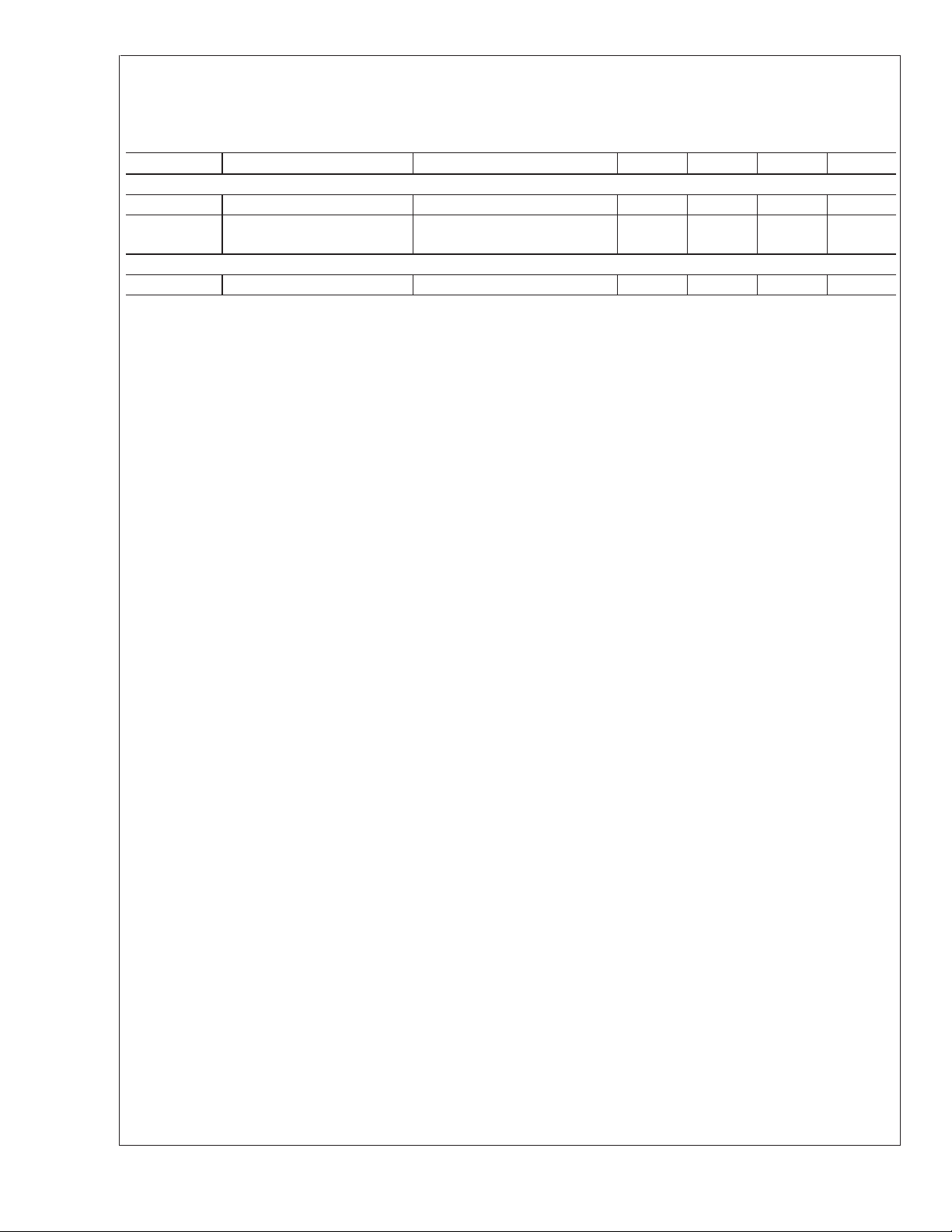
THERMAL CONTROLS
T
SD
T
SD-HYS
Thermal Shutdown Threshold 165 ˚C
Hysteresis for Thermal
10 ˚C
Shutdown
THERMAL RESISTANCE
θ
JA
Note 1: Absolute maximum ratings indicate limits beyond which damage to the device may occur. Operating Range indicates conditions for which the device is
intended to be functional, but does not guarantee specific performance limits. For guaranteed specifications and test conditions, see the Electrical Characteristics.
Note 2: The human body model is a 100 pF capacitor discharged through a 1.5 kΩ resistor into each pin. Test Method is per JESD22-AI14.
Note 3: V
Note 4: The enable pin is internally pulled up, so the LM2853 is automatically enabled unless an external enable voltage is applied.
Junction to Ambient MXA14A 38 ˚C/W
measured in a non-switching, closed-loop configuration at the SNS pin.
OUT
www.national.com 4
Page 5

LM2853
Typical Performance Characteristics Unless otherwise specified, the following conditions apply: V
= AVIN = PVIN = 5V, TJ= 25˚C.
Efficiency vs. I
V
OUT
Efficiency vs. I
V
OUT
LOAD
= 1.8V NFET R
20201507 20201505
LOAD
= 2.5V PFET R
vs. Temperature
DS(ON)
vs. Temperature
DS(ON)
IN
Efficiency vs. I
V
= 3.3V Switching Frequency vs. Temperature
OUT
20201509 20201504
LOAD
20201508 20201506
www.national.com5
Page 6

Typical Performance Characteristics Unless otherwise specified, the following conditions apply: V
= AVIN = PVIN = 5V, TJ= 25˚C. (Continued)
LM2853
I
vs. VINand Temperature ISDvs. VINand Temperature
Q
20201510 20201511
IN
www.national.com 6
Page 7

Block Diagram
LM2853
Applications Information
The LM2853 is a DC-DC buck regulator belonging to National Semiconductor’s synchronous SIMPLE SWITCHER
family. Integration of the PWM controller, power switches
and compensation network greatly reduces the component
count required to implement a switching power supply. A
typical application requires only four components: an input
capacitor, a soft-start capacitor, an output filter capacitor and
an output filter inductor.
INPUT CAPACITOR (C
Fast switching of large currents in the buck converter places
a heavy demand on the voltage source supplying PVIN. The
input capacitor, C
IN
needs to draw a burst of current from the supply. The RMS
current rating and the voltage rating of the C
therefore important in the selection of C
specification can be approximated by:
where D is the duty cycle, V
filtering of the supply. Trace resistance and inductance degrade the benefits of the input capacitor, so C
placed very close to PVIN in the layout. A 22 µF or 47 µF
ceramic capacitor is typically sufficient for C
with the large input capacitance a smaller capacitor should
be added such asa1µFceramic for higher frequency
filtering. Ceramic capacitors with high quality dielectrics such
as X5R or X7R should be used to provide a constant capacitance across temperature and line variations. For improved
)
IN
, supplies extra charge when the switcher
capacitor are
IN
. The RMS current
IN
OUT/VIN.CIN
also provides
should be
IN
. In parallel
IN
20201512
load regulation and transient performance, the use of a small
®
1 µF ceramic capacitor is also recommended as a local
bypass for the AVIN pin.
SOFT-START CAPACITOR (C
)
SS
The DAC that sets the reference voltage of the error amplifier sources a current through a resistor to set the reference
voltage. The reference voltage is one half of the output
voltage of the switcher due to the 200 kΩ divider connected
to the SNS pin. Upon start-up, the output voltage of the
switcher tracks the reference voltage with a two to one ratio
as the DAC current charges the capacitance connected to
the reference voltage node. Internal capacitance of 20 pF is
permanently attached to the reference voltage node which is
also connected to the soft start pin, SS. Adding a soft-start
capacitor externally increases the time it takes for the output
voltage to reach its final level. The charging time required for
the reference voltage can be estimated using the RC time
constant of the DAC resistor and the capacitance connected
to the SS pin. Three RC time constant periods are needed
for the reference voltage to reach 95% of its final value. The
actual start up time will vary with differences in the DAC
resistance and higher-order effects.
If little or no soft-start capacitance is connected, then the
start up time may be determined by the time required for the
current limit current to charge the output filter capacitance.
The capacitor charging equationI=C∆V/∆t can be used to
estimate the start-up time in this case. For example, a part
with a 3V output, a 100 µF output capacitance and a 5A
current limit threshold would require a time of 60 µs:
www.national.com7
Page 8

Applications Information (Continued)
LM2853
Since it is undesirable for the power supply to start up in
current limit, a soft-start capacitor must be chosen to force
the LM2853 to start up in a more controlled fashion based on
the charging of the soft-start capacitance. In this example,
supposea3msstart time is desired. Three time constants
are required for charging the soft-start capacitor to 95% of
the final reference voltage. So in this case RC = 1 ms. The
DAC resistor, R, is 450 kΩ so C can be calculated to be 2.2
nF. A 2.2 nF ceramic capacitor can be chosen to yield
approximatelya3msstart-up time.
SOFT-START CAPACITOR (C
CONDITIONS
Various fault conditions such as short circuit and UVLO of
the LM2853 activate internal circuitry designed to control the
voltage on the soft-start capacitor. For example, during a
short circuit current limit event, the output voltage typically
falls to a low voltage. During this time, the soft-start voltage
is forced to track the output so that once the short is removed, the LM2853 can restart gracefully from whatever
V
(V) VIN (V)
OUT
0.8 5 4.7 6.8 120 220 70 100
0.8 3.3 4.7 4.7 150 220 50 100
) AND FAULT
SS
TABLE 1. Recommended L
Min Max Min Max Min Max
voltage the output reached during the short circuit event. The
range of soft-start capacitors is therefore restricted to values
1nFto50nF.
COMPENSATION
The LM2853 provides a highly integrated solution to power
supply design. The compensation of the LM2853, which is
type-three, is included on-chip. The benefit of integrated
compensation is straight-forward, simple power supply design. Since the output filter capacitor and inductor values
impact the compensation of the control loop, the range of L
C
O
and C
values is restricted in order to ensure stability.
ESR
OUTPUT FILTER VALUES
Table 1 details the recommended inductor and capacitor
ranges for the LM2853 that are suggested for various typical
output voltages. Values slightly different than those recommended may be used, however the phase margin of the
power supply may be degraded. For best performance when
output voltage ripple is a concern, ESR values near the
minimum of the recommended range should be paired with
capacitance values near the maximum. If a minimum output
voltage ripple solution from a 5V input voltage is desired, a
6.8 µH inductor can be paired with a 220 µF (50 mΩ)
capacitor without degraded phase margin.
and COValues
O
(µH) CO(µF) C
L
O
ESR
(mΩ)
,
O
1 5 4.7 6.8 120 220 70 100
1 3.3 4.7 4.7 150 220 50 100
1.2 5 4.7 6.8 120 220 70 100
1.2 3.3 4.7 4.7 120 220 60 100
1.5 5 4.7 6.8 120 220 70 100
1.5 3.3 4.7 4.7 120 220 60 100
1.8 5 4.7 6.8 120 220 70 120
1.8 3.3 4.7 4.7 100 220 70 120
2.5 5 4.7 6.8 120 220 70 150
2.5 3.3 4.7 4.7 100 220 80 150
3.0 5 4.7 6.8 120 220 70 150
3.0 3.3 4.7 4.7 100 220 80 150
3.3 5 4.7 6.8 120 220 70 150
www.national.com 8
Page 9

Applications Information (Continued)
CHOOSING AN INDUCTANCE VALUE
The current ripple present in the output filter inductor is
determined by the input voltage, output voltage, switching
frequency and inductance according to the following equation:
where ∆ILis the peak to peak current ripple, D is the duty
cycle V
OUT/VIN,VIN
stage, V
OUT
switching frequency and L
filter inductor. Knowing the current ripple is important for
inductor selection since the peak current through the inductor is the load current plus one half the ripple current. Care
must be taken to ensure the peak inductor current does not
reach a level high enough to trip the current limit circuitry of
the LM2853. As an example, consider a 5V to 1.2V conversion and a 550 kHz switching frequency. According to Table
1, a 4.7 µH inductor may be used. Calculating the expected
peak-to-peak ripple,
Inductance Part Number Vendor
is the input voltage applied to the output
is the output voltage of the switcher, f is the
is the inductance of the output
O
TABLE 2. Recommended Inductors
4.7 µF DO3308P-472ML Coilcraft
4.7 µF DO3316P-472ML Coilcraft
4.7 µF MSS1260-472ML Coilcraft
5.2 µF MSS1038-522NL Coilcraft
5.6 µF MSS1260-562ML Coilcraft
6.8 µF DO3316P-682ML Coilcraft
6.8 µF MSS1260-682ML Coilcraft
The maximum inductor current for a 3A load would therefore
be 3A plus 177 mA, 3.177A. As shown in the ripple equation,
the current ripple is inversely proportional to inductance.
OUTPUT FILTER INDUCTORS
Once the inductance value is chosen, the key parameter for
selecting the output filter inductor is its saturation current
) specification. Typically I
(I
SAT
is given by the manufac-
SAT
turer as the current at which the inductance of the coil falls to
a certain percentage of the nominal inductance. The I
SAT
an inductor used in an application should be greater than the
maximum expected inductor current to avoid saturation. Below is a table of inductors that are suitable in LM2853
applications.
LM2853
of
OUTPUT FILTER CAPACITORS
The recommended capacitors that may be used in the output
Below are some examples of capacitors that can typically be
used in an LM2853 application.
filter with the LM2853 are limited in value and ESR range
according to Table 1.
TABLE 3. Recommended Capacitors
Capacitance (µF) Part Number Chemistry Vendor
100 594D107X_010C2T Tantalum Vishay-Sprague
100 593D107X_010D2_E3 Tantalum Vishay-Sprague
100 TPSC107M006#0075 Tantalum AVX
100 NOSD107M006#0080 Niobium Oxide AVX
100 NOSC107M004#0070 Niobium Oxide AVX
120 594D127X_6R3C2T Tantalum Vishay-Sprague
150 594D157X_010C2T Tantalum Vishay-Sprague
150 595D157X_010D2T Tantalum Vishay-Sprague
150 591D157X_6R3C2_20H Tantalum Vishay-Sprague
150 TPSD157M006#0050 Tantalum AVX
150 TPSC157M004#0070 Tantalum AVX
150 NOSD157M006#0070 Niobium Oxide AVX
220 594D227X_6R3D2T Tantalum Vishay-Sprague
220 591D227X_6R3D2_20H Tantalum Vishay-Sprague
220 591D227X_010D2_20H Tantalum Vishay-Sprague
220 593D227X_6R3D2_E3 Tantalum Vishay-Sprague
www.national.com9
Page 10

Applications Information (Continued)
LM2853
Capacitance (µF) Part Number Chemistry Vendor
220 TPSD227M006#0050 Tantalum AVX
220 NOSD227M0040060 Niobium Oxide AVX
TABLE 3. Recommended Capacitors (Continued)
SPLIT-RAIL OPERATION
The LM2853 can be powered using two separate voltages
for AVIN and PVIN. AVIN is the supply for the control logic;
PVIN is the supply for the power FETs. The output filter
SWITCH NODE PROTECTION
The LM2853 includes protection circuitry that monitors the
voltage on the switch pin. Under certain fault conditions,
switching is disabled in order to protect the switching devices. One side effect of the protection circuitry may be
observed when power to the LM2853 is applied with no or
light load on the output. The output will regulate to the rated
voltage, but no switching may be observed. As soon as the
output is loaded, the LM2853 will begin normal switching
operation.
LAYOUT GUIDELINES
These are several guidelines to follow while designing the
PCB layout for an LM2853 application.
1. The input bulk capacitor, C
, should be placed very
IN
close to the PVIN pin to keep the resistance as low as
possible between the capacitor and the pin. High current
levels will be present in this connection.
2. All ground connections must be tied together. Use a
broad ground plane, for example a completely filled back
plane, to establish the lowest resistance possible be-
components need to be chosen based on the value of PVIN.
For PVIN levels lower than 3.3V, use output filter component
values recommended for 3.3V. PVIN must always be equal
to or less than AVIN.
20201513
tween all ground connections.
3. The sense pin connection should be made as close to
the load as possible so that the voltage at the load is the
expected regulated value. The sense line should not run
too close to nodes with high dV/dt or dl/dt (such as the
switch node) to minimize interference.
4. The switch node connections should be low resistance
to reduce power losses. Low resistance means the trace
between the switch pin and the inductor should be wide.
However, the area of the switch node should not be too
large since EMI increases with greater area. So connect
the inductor to the switch pin with a short, but wide trace.
Other high current connections in the application such
as PVIN and V
assume the same trade off between
OUT
low resistance and EMI.
5. Allow area under the chip to solder the entire exposed
die attach pad to ground for improved thermal performance. Lab measurements also show improved regulation performance when the exposed pad is well
grounded.
LM2853 Example Circuit Schematic
FIGURE 1.
www.national.com 10
20201514
Page 11

LM2853 Example Circuit Schematic (Continued)
Bill of Materials for 5V to 3.3V Conversion
ID Part Number Type Size Parameters Qty Vendor
U
1
C
IN
C
BYP
C
SS
L
O
C
O
ID Part Number Type Size Parameters Qty Vendor
U
1
C
IN
C
BYP
CSS VJ0805Y222KXXA Capacitor 0603 2.2 nF 1 Vishay-Vitramon
L
O
C
O
LM2853MH-3.3 3A Buck ETSSOP-14 3.3V 1 NSC
GRM31CR60J476ME19 Capacitor 1206 47 µF 1 Murata
GRM21BR71C105KA01 Capacitor 0805 1 µF 1 Murata
VJ0805Y222KXXA Capacitor 0603 2.2 nF 1 Vishay-Vitramon
DO3316P-682 Inductor DO3316P 6.8 µH 1 Coilcraft
594D127X06R3C2T Capacitor C Case 120µF
1 Vishay-Sprague
(85mΩ)
Bill of Materials for 3.3V to 1.2V Conversion
LM2853MH-1.2 3A Buck ETSSOP-14 1.2V 1 NSC
GRM31CR60J476ME19 Capacitor 1206 47 µF 1 Murata
GRM21BR71C105KA01 Capacitor 0805 1 µF 1 Murata
DO3316P-472 Inductor DO3316P 4.7 µH 1 Coilcraft
NOSD157M006R0070 Capacitor D Case 150 µF
1AVX
(70 mΩ)
LM2853
www.national.com11
Page 12

Physical Dimensions inches (millimeters) unless otherwise noted
Buck Regulator
®
14-Lead ETSSOP Package
NS Package Number MXA14A
National does not assume any responsibility for use of any circuitry described, no circuit patent licenses are implied and National reserves
the right at any time without notice to change said circuitry and specifications.
For the most current product information visit us at www.national.com.
LIFE SUPPORT POLICY
NATIONAL’S PRODUCTS ARE NOT AUTHORIZED FOR USE AS CRITICAL COMPONENTS IN LIFE SUPPORT DEVICES OR SYSTEMS
WITHOUT THE EXPRESS WRITTEN APPROVAL OF THE PRESIDENT AND GENERAL COUNSEL OF NATIONAL SEMICONDUCTOR
LM2853 3A 550 kHz Synchronous SIMPLE SWITCHER
CORPORATION. As used herein:
1. Life support devices or systems are devices or systems
which, (a) are intended for surgical implant into the body, or
(b) support or sustain life, and whose failure to perform when
properly used in accordance with instructions for use
2. A critical component is any component of a life support
device or system whose failure to perform can be reasonably
expected to cause the failure of the life support device or
system, or to affect its safety or effectiveness.
provided in the labeling, can be reasonably expected to result
in a significant injury to the user.
BANNED SUBSTANCE COMPLIANCE
National Semiconductor follows the provisions of the Product Stewardship Guide for Customers (CSP-9-111C2) and Banned Substances
and Materials of Interest Specification (CSP-9-111S2) for regulatory environmental compliance. Details may be found at:
www.national.com/quality/green.
Lead free products are RoHS compliant.
National Semiconductor
Americas Customer
Support Center
Email: new.feedback@nsc.com
Tel: 1-800-272-9959
www.national.com
National Semiconductor
Europe Customer Support Center
Fax: +49 (0) 180-530 85 86
Email: europe.support@nsc.com
Deutsch Tel: +49 (0) 69 9508 6208
English Tel: +44 (0) 870 24 0 2171
Français Tel: +33 (0) 1 41 91 8790
National Semiconductor
Asia Pacific Customer
Support Center
Email: ap.support@nsc.com
National Semiconductor
Japan Customer Support Center
Fax: 81-3-5639-7507
Email: jpn.feedback@nsc.com
Tel: 81-3-5639-7560
 Loading...