

Datasheet LM2798MMX-1.8, LM2798MMX-1.5, LM2798MM-2.0, LM2798MM-1.8, LM2798MM-1.5 Datasheet (NSC)
...Page 1
April 2003
LM2797/LM2798
120mA High Efficiency Step-Down Switched Capacitor
Voltage Converter with Voltage Monitoring
LM2797/LM2798 120mA High Efficiency Step-Down Switched Capacitor Voltage Converter with
Voltage Monitoring
General Description
The LM2797/98 switched capacitor step-down DC/DC converters efficiently produce a 120mA regulated low-voltage
rail from a 2.6V to 5.5V input. Fixed output voltage options of
1.5V, 1.8V, and 2.0V are available. The LM2797/98 uses
multiple fractional gain configurations to maximize conversion efficiency over the entire input voltage and output current ranges. Also contributing to high overall efficiency is the
extremely low supply current of the LM2797/98: 35µA operating unloaded and 0.1µA in shutdown.
Features of the LM2797/98 include input voltage and output
voltage monitoring. Pin BATOK provides battery monitoring
by indicating when the input voltage is above 2.85V (typ.).
Pin POK verifies that the output voltage is not more than 5%
(typ.) below the nominal output voltage of the part.
The optimal external component requirements of the
LM2797/98 solution minimize size and cost, making the part
ideal for Li-Ion and other battery powered designs. Two 1µF
flying capacitors and two 10µF bypass capacitors are all that
is required, and no inductors are needed.
The LM2797/98 also features short-circuit protection overtemperature protection, and soft-start circuitry to prevent
excessive inrush currents. The LM2798 has a 400µs turn-on
time. The turn-on time of the LM2797 is 100µs.
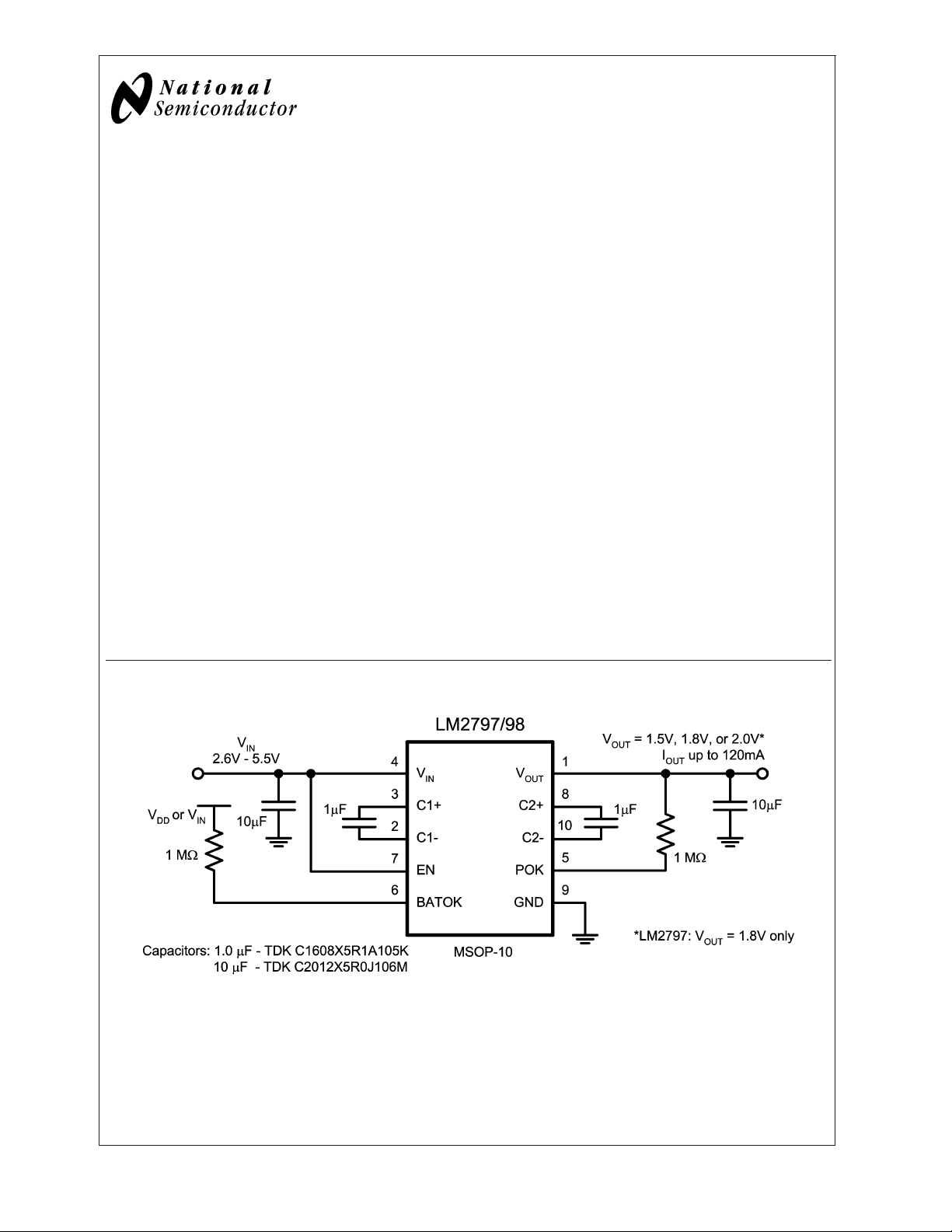
Typical Application Circuit
Features
n Output voltage options:
n 120mA output current capability
n Multi-Gain and Gain Hopping for Highest Possible
n 2.6V to 5.5V input range
n Input and Output Voltage Monitoring (BATOK and POK)
n Low operating supply current: 35µA
n Shutdown supply current: 0.1µA
n Thermal and short circuit protection
n LM2798 turn-on time: 400µs
n Available in an 10-Pin MSOP Package
±
5%, 1.8V±5%, and 1.5V±6%
2.0V
Efficiency - up to 90% Efficient
LM2797 turn-on time: 100µs
Applications
n Cellular Phones
n Pagers
n H/PC and P/PC Devices
n Portable Electronic Equipment
n Handheld Instrumentation
20044501
© 2003 National Semiconductor Corporation DS200445 www.national.com
Page 2
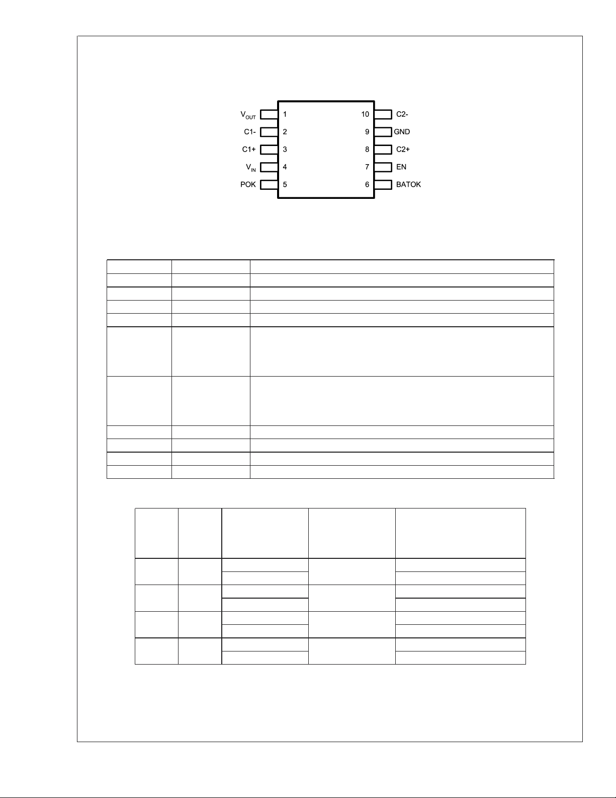
Connection Diagram
LM2797/LM2798
LM2797/98
Mini SO-10 (MSOP-10) Package
NS Package #: MUB10A
Pin Description
Pin Name Description
1V
OUT
2 C1- First Flying Capacitor: Negative Terminal
3 C1+ First Flying Capicitor: Positive terminal
4V
IN
5 POK Power-OK Indicator: Output voltage sense. Open-drain NFET output. With an
6 BATOK Battery-OK Indicator: Input voltage sense. Open-drain NFET output. With an
7 EN Enable Logic Input. High voltage = ON, Low voltage = SHUTDOWN
8 C2+ Second Flying Capacitor: Positive Terminal
9 GND Ground Connection
10 C2- Second Flying Capacitor: Negative Terminal
Ordering Information
Top View
20044502
Regulated Output Voltage
Input Voltage. Recommended VINRange: 2.6V to 5.5V
external pull-up resistor tied to POK, V(POK) will be high when V
regulating correctly. When V
falls out of regulation, the internal open-drain
OUT
OUT
FET pulls the POK voltage low.
external pull-up resistor tied to BATOK, V(BATOK) will be high when V
2.85V (typ). LM2797/98 pulls V(BATOK) low when V
<
2.65V (typ.) , and/or
IN
when the part is in shutdown [V(EN) = 0].
is
>
IN
Nominal
Output
Voltage
V
OUT(NOM)
1.80V 100µs
1.50V 400µs
1.80V 400µs
2.00V 400µs
www.national.com 2
Turn-on
Time
Order Number Package Marking Supplied As:
LM2797MM-1.8
LM2797MMX-1.8 3500 units on Tape-and-Reel
LM2798MM-1.5
LM2798MMX-1.5 3500 units on Tape-and-Reel
LM2798MM-1.8
LM2798MMX-1.8 3500 units on Tape-and-Reel
LM2798MM-2.0
LM2798MMX-2.0 3500 units on Tape-and-Reel
S80B
S56B
S57B
S58B
1000 units on Tape-and Reel
1000 units on Tape-and Reel
1000 units on Tape-and Reel
1000 units on Tape-and Reel
Page 3
LM2797/LM2798
Absolute Maximum Ratings (Notes 1,
2)
If Military/Aerospace specified devices are required,
please contact the National Semiconductor Sales Office/
Distributors for availability and specifications.
, EN, POK, BATOK pins: Voltage
V
IN
to Ground (Note 3) −0.3V to 5.6V
Junction Temperature (T
J-MAX-ABS
Continuous Power Dissipation
(Note 4) Internally Limited
V
Short-Circuit to GND Duration
OUT
(Note 4) Unlimited
Storage Temperature Range −65˚C to 150˚C
) 150˚C
Operating Ratings (Notes 1, 2)
Input Voltage Range 2.6V to 5.5V
Recommended Output Current
Range 0mA to 120mA
Junction Temperature Range -40˚C to 125˚C
Ambient Temperature Range
-40˚C to 85˚C
(Note 6)
Thermal Information
Thermal Resistance, MSOP-8 220˚C/W
Resistance, MSOP-8 Package
) (Note 7)
(θ
JA
Lead Temperature
(Soldering, 5 Sec.) 260˚C
ESD Rating (Note 5)
Human-body model:
Machine model
2kV
200V
Electrical Characteristics (Notes 2, 8)
Limits in standard typeface and typical values apply for TJ=25oC. Limits in boldface type apply over the operating junction
temperature range. Unless otherwise specified: 2.6 ≤ V
≤ 5.5V, V(EN) = VIN,C1=C2= 1µF, CIN=C
IN
Symbol Parameter Conditions Min Typ Max Units
LM2797-1.8, LM2798-1.8, LM2798-2.0
2.8V ≤ V
V
OUT
Output Voltage Tolerance
0mA ≤ I
4.2V
0mA ≤ I
IN
OUT
<
VIN≤ 5.5V
OUT
≤ 4.2V
≤ 120mA
≤ 120mA
-5 +5
-6 +6
LM2798-1.5
2.8V ≤ V
V
OUT
Output Voltage Tolerance
0mA ≤ I
4.2V
0mA ≤ I
IN
OUT
<
VIN≤ 5.5V
OUT
≤ 4.2V
≤ 120mA
≤ 120mA
-6 +6
-6 +6
All Output Voltage Options
I
I
V
E
E
t
f
I
Q
SD
R
PEAK
AVG
ON
SW
SC
Operating Supply Current I
= 0mA 35 50 µA
OUT
Shutdown Supply Current V(EN) = 0V 0.1 2 µA
Output Voltage Ripple LM2798-1.8: VIN= 3.6V, I
Peak Efficiency LM2798-1.8: VIN= 3.0V, I
Average Efficiency over
Li-Ion Input Voltage Range
(Note 11)
Turn-On Time LM2798, VIN=2.6V, I
LM2798-1.5: 3.0 ≤ V
LM2798-1.8: 3.0 ≤ V
LM2798-2.0: 3.0 ≤ V
LM2797, V
=2.6V, I
IN
IN
IN
IN
OUT
OUT
= 120mA 20 mV
OUT
= 60mA 90 %
OUT
≤ 4.2V, I
≤ 4.2V, I
≤ 4.2V, I
= 60mA 76 %
OUT
= 60mA 82
OUT
= 60mA 75
OUT
=100mA, (Note 12) 400 µs
=100mA, (Note 12) 100
Switching Frequency 500 kHz
Short-Circuit Current VIN= 3.6, V
=0V 25 mA
OUT
Enable Pin (EN) Characteristics
V
IH
V
IL
I
EN
EN pin Logic-High Input 0.9 V
EN pin Logic-Low Input 0 0.4 V
=0V 0 nA
V
EN pin input current
EN
V
= 5.5V 30
EN
= 10µF. (Note 9)
OUT
IN
%of
V
OUT(nom)
(Note 10)
%of
V
OUT(nom)
(Note 10)
p-p
V
www.national.com3
Page 4
Electrical Characteristics (Notes 2, 8) (Continued)
Limits in standard typeface and typical values apply for TJ=25oC. Limits in boldface type apply over the operating junction
temperature range. Unless otherwise specified: 2.6 ≤ V
≤ 5.5V, V(EN) = VIN,C1=C2= 1µF, CIN=C
IN
Symbol Parameter Conditions Min Typ Max Units
POK Characteristics
LM2797/LM2798
V
T-POK
Threshold of output voltage
for POK transition
POK transition L to H 95 99
POK transition H to L 83 92
Hysterisis 3
I
POK-H
V
POK-L
POK-high leakage current V(POK) = 3.6V 1 5 µA
POL-low pull-down voltage I(POK) = -100µA 200 300 mV
BATOK Characteristics
V
T-BATOK
Input voltage threshold for
BATOK transition
BATOK transition L to H 2.85 3.0 V
BATOK transition H to L 2.4 2.65
Hysterisis 0.20
I
BATOK-H
BATOK-high leakage
V(BATOK) = 3.6V 1 5 µA
current
V
BATOK-L
BATOK-low pull-down
I(BATOK) = - 100µA 200 300 mV
voltage
Note 1: Absolute Maximum Ratings indicate limits beyond which damage to the component may occur. Operating Ratings are conditions under which operation of
the device is guaranteed. Operating Ratings do not imply guaranteed performance limits. For guaranteed performance limits and associated test conditions, see the
Electrical Characteristics tables.
Note 2: All voltages are with respect to the potential at the GND pin.
Note 3: Voltage on the EN pin must not be brought above V
Note 4: Thermal shutdown circuitry protects the device from permanent damage.
Note 5: The human-body model is a 100 pF capacitor discharged through a 1.5kΩ resistor into each pin. The machine model is a 200pF capacitor discharged
directly into each pin.
Note 6: Maximum ambient temperature (T
dissipation of the device in the application (P
following equation: T
outside the listed T
Note 7: Junction-to-ambient thermal resistance is highly dependent on application conditions and PC board layout. In applications where high maximum power
dissipation exists, special care must be paid to thermal dissipation issues. For more information on these topics, please refer to the Power Dissipation section of
this datasheet.
Note 8: All room temperature limits are 100% tested or guaranteed through statistical analysis. All limits at temperature extremes are guaranteed by correlation
using standard Statistical Quality Control methods (SQC). All limits are used to calculate Average Outgoing Quality Level (AOQL). Typical numbers are not
guaranteed, but do represent the most likely norm.
Note 9: C
Note 10: V
Note 11: Efficiency is measured versus V
Weighting to account for battery voltage discharge characteristics (V
Note 12: Turn-on time is measured from when the EN signal is pulled high until the output voltage crosses 90% of its final value. Resistive load used for startup
measurement, with value chosen to give I
A
IN,COUT,C1
OUT (NOM)
A-MAX=TJ-MAX-OP
rating so long as the junction temperature of the device does not exceed the maximum operating rating of 125oC.
, and C2: Low-ESR Surface-Mount Ceramic Capacitors (MLCCs) used in setting electrical characteristics
is the nominal output voltage of the part. An example: V
-(θJAxP
) is dependent on the maximum operating junction temperature (T
A-MAX
), and the junction-to ambient thermal resistance of the part/package in the application (θJA), as given by the
D-MAX
D-MAX
, with VINbeing swept in small increments from 3.0V to 4.2V. The average is calculated from these measurement results.
IN
= 100mA when the output voltage is fully established.
OUT
+ 0.3V.
IN
J-MAX-OP
). The ambient temperature operating rating is provided merely for convenience. This part may be operated
of LM2798MM-1.8 is 1.8V.
OUT-NOM
vs. Time) is not done in computing the average.
BAT
= 10µF. (Note 9)
OUT
= 125oC), the maximum power
%of
V
OUT-NOM
(Note 10)
www.national.com 4
Page 5
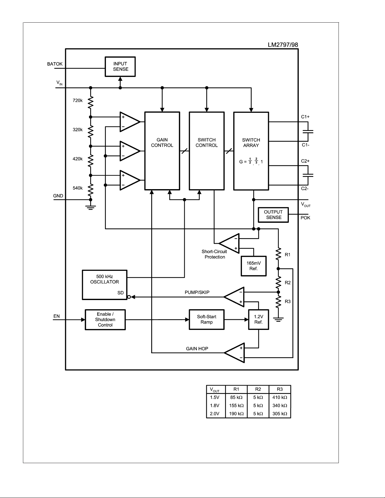
Block Diagram
LM2797/LM2798
20044503
www.national.com5
Page 6

Typical Performance Characteristics Unless otherwise specified: C
1.0µF C
LM2797/LM2798
= 10µF, TA=25oC. Capacitors are low-ESR multi-layer ceramic capacitors (MLCC’s).
OUT
Output Voltage vs. Input Voltage:
Output Voltage vs. Input Voltage:
LM2798-1.5 (1mA)
20044507 20044508
= 10µF, C1 = 1.0µF, C2 =
IN
LM2798-1.5 (120mA)
Output Voltage vs. Input Voltage:
LM2797/98-1.8 (1mA)
Output Voltage vs. Input Voltage:
LM2798-2.0 (1mA)
Output Voltage vs. Input Voltage:
LM2797/98-1.8 (120mA)
20044509 20044510
Output Voltage vs. Input Voltage:
LM2798-2.0 (120mA)
20044511 20044512
www.national.com 6
Page 7

LM2797/LM2798
Typical Performance Characteristics Unless otherwise specified: C
1.0µF C
= 10µF, TA=25oC. Capacitors are low-ESR multi-layer ceramic capacitors (MLCC’s). (Continued)
OUT
= 10µF, C1 = 1.0µF, C2 =
IN
Efficiency vs. Input Voltage: LM2798-1.5 Efficiency vs. Output Current: LM2798-1.5
20044513
Efficiency vs. Input Voltage: LM2797/98-1.8 Efficiency vs. Output Current: LM2797/98-1.8
20044514
20044515
20044516
Efficiency vs. Input Voltage: LM2798-2.0 Effiency vs. Output Current: LM2798-2.0
20044517
20044518
www.national.com7
Page 8

Typical Performance Characteristics Unless otherwise specified: C
1.0µF C
LM2797/LM2798
= 10µF, TA=25oC. Capacitors are low-ESR multi-layer ceramic capacitors (MLCC’s). (Continued)
OUT
Output Voltage Ripple vs. Output Current Output Voltage Ripple vs. Input Voltage
20044521 20044519
Output Voltage Ripple Short Circuit Current
= 10µF, C1 = 1.0µF, C2 =
IN
20044506
Start Up Waveform: LM2798-1.8 Transient Load Response
20044504 20044505
20044520
www.national.com 8
Page 9

Operation Description
OVERVIEW
The LM2797/98 are switched capacitor converters that produce a regulated low-voltage output. The core of the parts is
a highly efficient charge pump that utilizes multiple fractional
gains and pulse-frequency modulated (PFM) switching to
minimize power losses over wide input voltage and output
current ranges. A description of the principal operational
characteristics of the LM2797/98 is broken up into the following sections: PFM Regulation, Fractional Multi-Gain
Charge Pump, and Gain Selection for Optimal Efficiency.
Each of these sections refers to the block diagram presented
on the previous page.
PFM REGULATION
The LM2797/98 achieves tightly regulated output voltages
with pulse-frequency modulated (PFM) regulation. PFM simply means the part only pumps when it needs to. When the
output voltage is above the target regulation voltage, the part
idles and consumes minimal supply-current. In this state, the
load current is supplied solely by the charge stored on the
output capacitor. As this capacitor discharges and the output
voltage falls below the target regulation voltage, the charge
pump activates. Charge/current is delivered to the output
(supplying the load and boosting the voltage on the output
capacitor).
The primary benefit of PFM regulation is when output currents are light and the part is predominantly in the lowsupply-current idle state. Net supply current is minimal because the part only occasionally needs to recharge the
output capacitor by activating the charge pump.
FRACTIONAL MULTI-GAIN CHARGE PUMP
The core of the LM2797/98 is a two-phase charge pump
controlled by an internally generated non-overlapping clock.
The charge pump operates by using the external flying capacitors, C1 and C2, to transfer charge from the input to the
output. During the charge phase, which doubles as the PFM
"idle state", the flying capacitors are charged by the input
supply. The charge pump will be in this state until the output
voltage drops below the target regulation voltage, triggering
the charge pump to activate so that it can deliver charge to
the output. Charge transfer is achieved in the pump phase.
In this phase, the fully charged flying capacitors are connected to the output so that the charge they hold can supply
the load current and recharge the output capacitor.
Input, output, and intermediary connections of the flying
capacitors are made with internal MOS switches. The
LM2797/98 utilizes two flying capacitors and a versatile
switch network to achieve several fractional voltage gains:
1
⁄2,2⁄3, and 1. With this gain-switching ability, it is as if the
LM2797/98 is three-charge-pumps-in-one. The "active"
charge pump at any given time is the one that will yield the
highest efficiency given the input and output conditions
present.
I
=GxI
E=(V
OUTxIOUT
IN
)÷(VINxIIN)=V
OUT
÷(GXVIN)
OUT
In the equations, G represents the charge pump gain. Efficiency is at its highest as GxV
approaches V
IN
OUT
. Optimal
efficiency is achieved when gain is able to adjust depending
on input and output voltage conditions. Due to the nature of
charge pumps, G cannot adjust continuously, which would
be ideal from an efficiency standpoint. But G can be a set of
simple quantized ratios, allowing for a good degree of efficiency optimization.
The gain set of the LM2797/98 consists of the gains 1/2, 2/3,
and 1. An internal input voltage range detector, along with
the nominal output voltage of a given LM2797/98 option,
determines what is to be referred to as the "base gain" of the
part, G
the part over a set V
. The base gain is the default gain configuration of
B
range. Table 1 lists GBof the LM2798-
IN
1.8 over the input voltage range. For the remainder of this
discussion, the 1.8V option of the LM2798 will be used as an
example. The other voltage options of the LM2798 operate
under the same principles as LM2798-1.8, the gain transitions merely occur at different input voltages. Since the only
difference between the LM2797 and the LM2798 is start-up
time, the modes of operation of the LM2798-1.8 discussed
here are identical to those of the LM2797-1.8.
TABLE 1. LM2798-1.8 Base Gain (G
) vs. V
B
IN
Input Voltage Base Gain (GB)
2.6V - 2.9V 1
2.9V - 3.8V
3.8V - 5.5V
2
⁄
3
1
⁄
2
Figure 1 shows the efficiency of the LM2798-1.8 versus input
voltage, with output currents of 10mA and 120mA. The base
gain regions (G
set of ideal efficiency gradients, E
) are separated and labeled. There is also a
B
IDEAL(G=xx)
, showing the
ideal efficiency of a charge pumps with gains of 1/2, 2/3, and
1. These gradients have been generated using the ideal
efficiency equation presented above.
LM2797/LM2798
GAIN SELECTION AND GAIN HOPPING FOR OPTIMAL EFFICIENCY
The ability to switch gains based on input and output conditions results in optimal efficiency throughout the operating
ranges of the LM2797/98. Charge-pump efficiency is derived
in the following two ideal equations (supply current and other
losses are neglected for simplicity):
20044522
FIGURE 1. Efficiency of LM2798-1.8 with 10mA and
120mA output currents. Base-gain (G
) regions are
B
separated and labeled. Ideal efficiency curves of
charge pumps with G =1/2, 2/3, and 1 are included,
and are labelled:
E
IDEAL(G=1),EIDEAL(G=2/3),EIDEAL(G=1/2)
www.national.com9
Page 10

Operation Description (Continued)
The 10mA load curve in Figure 1 gives a clear picture of how
base-gain affects overall converter efficiency. The "ideal efficiency gradients" in the figure show the efficiency of ideal
switched capacitor converters with gains of 1, 2/3, and 1/2,
LM2797/LM2798
respectively. The 10mA-load efficiency curve closely follows
the ideal efficiency gradients in each of the respective basegain regions. At the base-gain transitions (V
there are sharp transitions in the 10mA curve because the
LM2797/98 switches base-gains. With a 10mA output current there is very little gain hopping (described below), and
the gain of the LM2798-1.8 is equal to the base-gain over the
entire operating input voltage range. Internal supply current
has a minimal impact on efficiency with a 10 mAload. Supply
current does have a small effect, and it the reason why the
10mA load curve is slightly below the ideal efficiency gradients in each of the base-gain regions. But overall, due to the
lack of gain hopping and the minimal impact of supply current on converter efficiency, the 10mA load curve very
closely mirrors the ideal efficiency curves in each of the
respecitve base-gain regions.
The 120mA-load curve in Figure 1 illustrates the effect of
gain hopping on converter efficiency. Gain hopping is implemented to overcome output voltage droop that results from
charge-pump non-idealities. In an ideal charge pump, the
output voltage is equal to the product of the gain and the
input voltage. Non-idealities such as finite switch resistance,
capacitor ESR, and other factors result in the output of
practical charge pumps being below the ideal value. This
output droop is typically modeled as an output resistance,
, because the magnitude of the droop increases lin-
R
OUT
early with load current.
Ideal Charge Pump: V
Real Charge Pump: V
OUT
OUT
=(GxVIN)-(I
The LM2797/98 compensates for output voltage droop under high load conditions by gain hopping. When the basegain is not sufficient to keep the output voltage in regulation,
the part will temporarily hop up to the next highest gain
setting to provide an intermittent boost in output voltage.
When the output voltage is sufficiently boosted, the gain
configuration reverts back to the base-gain setting. An example: if the input voltage of the LM2798-1.8 is 3.2V, the part
is in the 2/3 base-gain region. If the output voltage droops,
the gain configuration will temporarily hop up to a gain of 1.
It will operate with a gain of 1 until the nominal output voltage
is restored, at which time the gain will hop back down to 2/3.
If the load remains high, the part will continue to hop back
and forth between the base-gain and the next highest gain
setting, and the output voltage will remain in regulation. In
contrast to the base-gain decision, which is made based on
the input voltage, the decision to gain hop is made by
monitoring the voltage at the output of the part.
TABLE 3. Typical POK functionality, with 1MΩ pull-up resistor connected between POK and V
V
IN
>
1.7V H
>
1.7V H ≤ 92% OF V
>
1.7V L X LOW ON 0V
<
1.7V X X LOW OFF 0V, (V
EN V
>
95% of V
OUT
IN
=GxV
OUTxROUT
OUT-nom
OUT-nom
The 120mA-load efficiency curve in Figure 1 illustrates the
effect of gain hopping on efficiency. Comparing the 120mA
load curve to the 10mA load curve, notice that to the right of
the base-gain transitions the efficiency of the 120mA curve
increases gradually. In contrast, the 10mA curve makes a
very sharp transition. The base-gain of both curves is the
same for both loads. The difference comes in gain hopping.
With the 120mA load, the part operates in the base-gain
= 2.9V, 3.8V),
setting for a certain percentage of time and in the nexthighest gain setting for the remainder. The percentage of
time spent in an elevated gain configuration decreases as
the input voltage rises, as less gain-hopping boost is required with increased input voltage. When the input voltage
in a given base-gain region is large enough so that no extra
boost from gain hopping is required, the part operates entirely in the base gain region. This can be seen in the figure
where the 120mA-load efficiency curve follows the ideal
efficiency gradients.
TABLE 2. LM2798-1.8 Gain Hopping Regions
Input Voltage
3.0V - 3.3V
3.8V - 4.4V
Base Gain
)
(G
B
2
⁄
3
1
⁄
2
Gain hopping contributes to the overall high efficiency of the
LM2797/98. Gain hopping only occurs when required to
keep the output voltage in regulation. This allows the
LM2797/98 to operate in the higher efficiency base-gain
setting as much as possible. Gain hopping also allows the
base-gain transitions to be placed at input voltages that are
as low as practically possible. Doing so maximizes the peaks
IN
)
and minimizes the valleys of the efficiency "saw-tooth"
curves, maximizing total solution efficiency.
POK: OUTPUT VOLTAGE STATUS INDICATOR
The POK pin is an NMOS-open-drain-logic signal that indicates when the output voltage of the LM2797/98 is at or
above 95% (typ) of the target output voltage. To function
properly, the POK pin must be connected to a pull-up resistor
(1MΩ (typ.)), or other pull-up device. With a pull-up in place,
V(POK) will be HIGH when V
the nominal output voltage (V
is at or above 95% (typ) of
OUT
OUT-nom
depending on voltage option). If the output falls below 92%
(typ.) of the nominal output voltage, V(POK) will be 0V. There
is hysteresis of 3% between the thresholds. The POK function is disabled and V(POK) is pulled down to 0V when the
LM2797/98 is in shutdown (EN = 0V). Table 3 is a complete
list of the typical POK regions of operation.
POK State Internal POK Transistor State V(POK)
HIGH OFF V
LOW ON 0V
Gain Hop
Setting
1
2
⁄
3
= 1.5V, 1.8V, or 2.0V,
OUT
OUT
off)
OUT
www.national.com 10
Page 11

Operation Description (Continued)
LM2797/LM2798
TABLE 4. Typical BATOK functionality, with 1MΩ pull-up resistor connected between BATOK and V
V
IN
>
2.85V H HIGH OFF V
>
1.1V,<2.65V H LOW ON 0V
>
1.1V L LOW ON 0V
EN
BATOK State Internal BATOK
≤ 1.1V X LOW OFF V
BATOK: INPUT VOLTAGE STATUS INDICATOR
The BATOK pin is an NMOS-open-drain-logic signal that
indicates the status of the input voltage. To function properly,
the BATOK pin must be connected to a pull-up resistor, or
other pull-up device. With a pull-up in place, V(BATOK) will
be HIGH when V
is at or above 2.85V. If the output falls
IN
below 2.65V (typ.), V(BATOK) will be 0V. There is hysteresis
of 20mV (typ.) between the thresholds. The BATOK function
is disabled and V(BATOK) is pulled down to 0V when the
LM2797/98 is in shutdown (EN = 0V). Table 4 is a complete
list of the typical BATOK regions of operation.
SHUTDOWN
The LM2797/98 is in shutdown mode when the voltage on
the active-low logic enable pin (EN) is low. In shutdown, the
LM2797/98 draws virtually no supply current. When in shutdown, the output of the LM2797/98 is completely disconnected from the input, and will be 0V unless driven by an
outside source.
In some applications, it may be desired to disable the
LM2797/98 and drive the output pin with another voltage
source. This can be done, but the voltage on the output pin
of the LM2797/98 must not be brought above the input
voltage. The output pin will draw a small amount of current
when driven externally due the internal feedback resistor
divider connected between V
OUT
and GND.
SOFT START
The LM2797/98 employs soft start circuitry to prevent excessive input inrush currents during startup. At startup, the
output voltage gradually rises from 0V to the nominal output
voltage. This occurs in 400µs (typ.) with the LM2798.
Turn-on time of the LM2797 is 100µs (typ.). Soft-start is
engaged when the part is enabled, including situations
where voltage is established simultaneously on the V
and
IN
EN pins.
THERMAL SHUTDOWN
Protection from overheating-related damage is achieved
with a thermal shutdown feature. When the junction temperature rises to 150
o
C (typ.), the part switches into shutdown mode. The LM2797/98 disengages thermal shutdown
when the junction temperature of the part is reduced to
o
C (typ.). Due to its high efficiency, the LM2797/98
130
should not activate thermal shutdown (or exhibit related
thermal cycling) when the part is operated within specified
input voltage, output current, and ambient temperature operating ratings.
IN
V(BATOK)
Transistor State
IN
, ≤ 1.1V
IN
SHORT-CIRCUIT PROTECTION
The LM2797/98 short-circuit protection circuitry protects the
device in the event of excessive output current and/or output
shorts to ground. A graph of "Short-Circuit Current vs. Input
Voltage" is provided in the Performance Characteristics
section.
Application Information
OUTPUT VOLTAGE RIPPLE
The voltage ripple on the output of the LM2797/98 is highly
dependent on application conditions. The output capacitor,
the input voltage, and the output current each play a significant part in determining the output voltage ripple. Due to the
complexity of LM2797/98 operation, providing equations or
models to approximate the magnitude of the ripple cannot be
easily accomplished. The following general statements can
be made, however
The output capacitor will have a significant effect on output
voltage ripple magnitude. Ripple magnitude will typically be
linearly proportional to the output capacitance present. A
low-ESR ceramic capacitor is recommended on the output to
keep output voltage ripple low. Placing multiple capacitors in
parallel can reduce ripple significantly. Doing this increases
capacitance and reduces ESR (the effective net ESR is
governed by the properties of parallel resistance). Placing
two identical capacitors in parallel have twice the capacitance and half the ESR, as compared to one of these capacitors all by itself. Similarly, if a large-value, high-ESR
capacitor (tantalum, for example) is to be used as the primary output capacitor, the net output ESR can be significantly reduced by placing a low-ESR ceramic capacitor in
parallel with this primary output capacitor.
Ripple is increased when the LM2797/98 is gain hopping.
With high output currents, ripple is likely to vary significantly
with input voltage, depending on whether on not the part is
gain hopping.
CAPACITORS
The LM2797/98 requires 4 external capacitors for proper
operation. Surface-mount multi-layer ceramic capacitors are
recommended. These capacitors are small, inexpensive and
have very low equivalent series resistance (ESR, ≤ 15mΩ
typ.). Tantalum capacitors, OS-CON capacitors, and aluminum electrolytic capacitors generally are not recommended
for use with the LM2797/98 due to their high ESR, as compared to ceramic capacitors.
For most applications, ceramic capacitors with an X7R or
X5R temperature characteristic are preferred for use with the
LM2797/98. These capacitors have tight capacitance tolerance (as good as
ture (X7R:
o
Cto85oC).
-55
±
10%) and hold their value over tempera-
±
15% over -55oCto125oC; X5R:±15% over
www.national.com11
Page 12

Application Information (Continued)
Capacitors with a Y5V or Z5U temperature characteristic are
generally not recommended for use with the LM2797/98.
These types of capacitors typically have wide capacitance
tolerance (+80%, -20%) and vary significantly over tempera-
LM2797/LM2798
ture (Y5V: +22%, -82% over -30
+22%, -56% over +10
o
Cto+85oC range). Under some conditions, a 1µF-rated Y5V or Z5U capacitor could have a
capacitance as low as 0.1µF. Such detrimental deviation is
likely to cause these Y5V and Z5U capacitors to fail to meet
the minimum capacitance requirements of the LM2797/98.
The table below lists some leading ceramic capacitor manufacturers.
Manufacturer Contact Information
AVX www.avx.com
Murata www.murata.com
Taiyo-Yuden www.t-yuden.com
TDK www.component.tdk.com
Vishay-Vitramon www.vishay.com
o
Cto+85oC range; Z5U:
Low-ESR ceramic capacitors with X7R or X5R temperature
characteristic are strongly recommended for use here. The
flying capacitors C1 and C2 should be identical. As a general
rule, the capacitance value of each flying capacitor should
be 1/10th that of the output capacitor. ESR should be as low
as possible to minimize the output resistance of the charge
pump and give maximum output current capability. Polarized
capacitor (tantalum, aluminum electrolytic, etc.) must not be
used for the flying capacitors, as they could become reversebiased upon start-up of the LM2797/98.
INPUT CAPACITOR
The input capacitor (C
) is a reservoir of charge that aids a
IN
quick transfer of charge from the supply to the flying capacitors during the charge phase of operation. The input capacitor helps to keep the input voltage from drooping at the start
of the charge phase when the flying capacitor is connected
to the input, and helps to filter noise on the input pin that
could adversely affect sensitive internal analog circuitry biased off the input line. An X7R/X5R ceramic capacitor is
recommended for use. As a general recommendation, the
input capacitor should be chosen to match the output capacitor.
OUTPUT CAPACITOR
The output capacitor of the LM2797/98 greatly affect performance of the circuit. In typical high-current applications, a
10µF low-ESR (ESR = equivalent series resistance) ceramic
capacitor is recommended. For lighter loads, the output
capacitance may be reduced (as low as 1µF for output
currents ≤ 60mA is usually acceptable). The performance of
the part should be evaluated with special attention paid to
efficiency and output ripple to ensure the capacitance chosen on the output yields performance suitable for the application. In extreme cases, excessive ripple could cause control loop instability, severely affecting the performance of the
part. If excessive ripple is present, the output capacitance
should be increased.
The ESR of the output capacitor affects charge pump output
resistance, which plays a role in determining output current
capability. Both output capacitance and ESR affect output
voltage ripple (See Output Voltage Ripple section, above).
For these reasons, a low-ESR X7R/X5R ceramic capacitor is
the capacitor of choice for the LM2797/98 output.
FLYING CAPACITORS
The flying capacitors (C
and C2) transfer charge from the
1
input to the output, and determine the strength of the charge
pump: the larger the capacitance, the greater the output
current capability. If capacitors are too small, the LM2797/98
could spend excessive amount of time gain hopping: decreasing efficiency, increasing output voltage ripple, and
possibly impeding the ability of the part to regulate. On the
other hand, if the flying capacitors are too large they could
potentially overwhelm the output capacitor, resulting in increased output voltage ripple.
POWER DISSIPATION
LM2797/98 power dissipation will, typically, not be much of a
concern in most applications. Derating to accommodate selfheating will rarely be required due to the high efficiency of
the part. Peak power dissipation (P
tions is seen with the LM2798-1.5 operating at V
and I
= 120mA (conditions limited to valid operating
OUT
) of all LM2797/98 op-
D
IN
= 5.5V
ratings). Under these conditions, the power efficiency (E) of
the LM2798-1.5 is 54% (typ.). Assuming a typical junctionto-ambient thermal resistance (θ
of 220˚C/Watt, the junction temperature (T
) for the MSOP package
JA
) of the part is
J
calculated below for a part operating at the maximum rated
OUT
OUT
) of 85˚C.
A
ambient temperature (T
P
D=PIN-POUT
=(P
OUT
/E)-P
= [(1/E) - 1] x P
= [(1/64%) - 1] x 1.5V x 120mW
= 153mW
J=TA
=(PDx θJA)
T
= 85˚C + (.153W x 220˚C/W)
=119˚C
Even under these peak power dissipation and ambient temperature conditions, the junction temperature of the LM2798-
1.5 is below the maximum operating rating of 125˚C.
As an additional note, the ambient temperature operating
rating range listed in the specifications is provided merely for
convenience. The LM2797/98 may be operated outside this
rating, so long as the junction temperature of the device
does not exceed the maximum operating rating of 125˚C.
www.national.com 12
Page 13

Layout Guidelines
Proper board layout to accommodate the LM2797/98 circuit
will help to ensure optimal performance. The following guidelines are recommended:
Place capacitors as close to the LM2797/98 as possible,
•
and preferably on the same side of the board as the IC.
Use short, wide traces to connect the external capacitors
•
to the LM2797/98 to minimize trace resistance and inductance.
FIGURE 2. Sample single-layer board layout of the LM2797/98 Typical Application Circuit
(Vias to a ground plane, assumed to be present, are located in the center of the LM2797/98 footprint.)
Use a low resistance connection between ground and the
•
GND pin of the LM2797/98. Using wide traces and/or
multiple vias to connect GND to a ground plane on the
board is most advantageous.
Figure 2 is a sample single-layer board layout that accommodates the LM2797/98 typical application circuit, as pictured on the cover of this datasheet
20044524
LM2797/LM2798
www.national.com13
Page 14

Physical Dimensions inches (millimeters) unless otherwise noted
Voltage Monitoring
LM2797/LM2798 120mA High Efficiency Step-Down Switched Capacitor Voltage Converter with
Mini SOP-10 (MSOP-10)
MUB10A
LIFE SUPPORT POLICY
NATIONAL’S PRODUCTS ARE NOT AUTHORIZED FOR USE AS CRITICAL COMPONENTS IN LIFE SUPPORT
DEVICES OR SYSTEMS WITHOUT THE EXPRESS WRITTEN APPROVAL OF THE PRESIDENT AND GENERAL
COUNSEL OF NATIONAL SEMICONDUCTOR CORPORATION. As used herein:
1. Life support devices or systems are devices or
systems which, (a) are intended for surgical implant
into the body, or (b) support or sustain life, and
whose failure to perform when properly used in
accordance with instructions for use provided in the
2. A critical component is any component of a life
support device or system whose failure to perform
can be reasonably expected to cause the failure of
the life support device or system, or to affect its
safety or effectiveness.
labeling, can be reasonably expected to result in a
significant injury to the user.
National Semiconductor
Americas Customer
Support Center
Email: new.feedback@nsc.com
Tel: 1-800-272-9959
www.national.com
National Semiconductor
Europe Customer Support Center
Fax: +49 (0) 180-530 85 86
Email: europe.support@nsc.com
Deutsch Tel: +49 (0) 69 9508 6208
English Tel: +44 (0) 870 24 0 2171
Français Tel: +33 (0) 1 41 91 8790
National Semiconductor
Asia Pacific Customer
Support Center
Fax: +65-6250 4466
Email: ap.support@nsc.com
Tel: +65-6254 4466
National Semiconductor
Japan Customer Support Center
Fax: 81-3-5639-7507
Email: jpn.feedback@nsc.com
Tel: 81-3-5639-7560
National does not assume any responsibility for use of any circuitry described, no circuit patent licenses are implied and National reserves the right at any time without notice to change said circuitry and specifications.
 Loading...