

Page 1
LM2794/LM2795
Current Regulated Switched Capacitor LED Supply with
Analog and PWM Brightness Control
General Description
The LM2794/95 is a fractional CMOS charge-pump that
provides four regulated current sources. It accepts an input
voltage range from 2.7V to 5.5V and maintains a constant
current determined by an external sense resistor.
The LM2794/5 delivers up to 80mA of load current to accommodate four White LEDs. The switching frequency is
325kHz. (min.) to keep the conducted noise spectrum away
from sensitive frequencies within portable RF devices.
Brightness can be controlled by both linear and PWM techniques. A voltage between 0V and 3.0V may be applied to
the BRGT pin to linearly vary the LED current. Alternatively,
a PWM signal can be applied to the SD pin to vary the
perceived brightness of the LED. The SD pin reduces the
operating current to 2.3µA (typ.) The LM2794 is shut down
when the SD pin is low, and the LM2795 is shut down when
the SD pin is high.
The LM2794/95 is available in a micro SMD-14 CSP package.
Features
n Regulated current sources with±0.5% matching
between any two outputs
n High efficiency 3/2 boost function
n Drives one, two, three or four white LEDs
n 2.7V to 5.5V Input Voltage
n Up to 80mA output current
n Analog brightness control
n Active-low or high shutdown input (’94/95)
n Very small solution size and no inductor
n 2.3µA (typ.) shutdown current
n 325kHz switching frequency (min.)
n Constant Frequency generates predictable noise
spectrum
n Standard Micro SMD-14 package: 2.08mm X 2.403mm
X 0.845mm High
n Thin Micro SMD-14 package: 2.08mm X 2.403mm X
0.600mm High
Applications
n White LED Display Backlights
n White LED Keypad Backlights
n 1-Cell Li-Ion battery-operated equipment including
PDAs, hand-held PCs, cellular phones
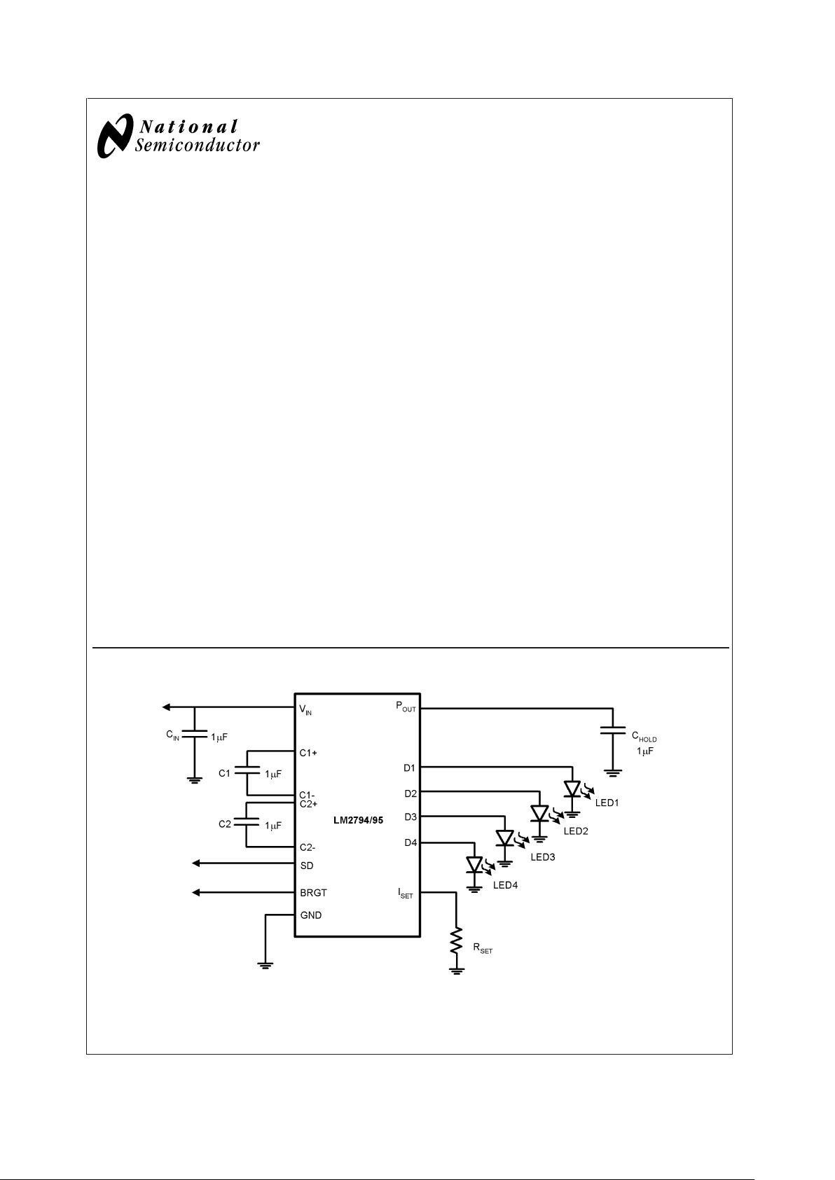
Basic Application Circuit
20028503
May 2003
LM2794/LM2795 Current Regulated Switched Capacitor LED Supply with Analog and PWM
Brightness Control
© 2003 National Semiconductor Corporation DS200285 www.national.com
Page 2
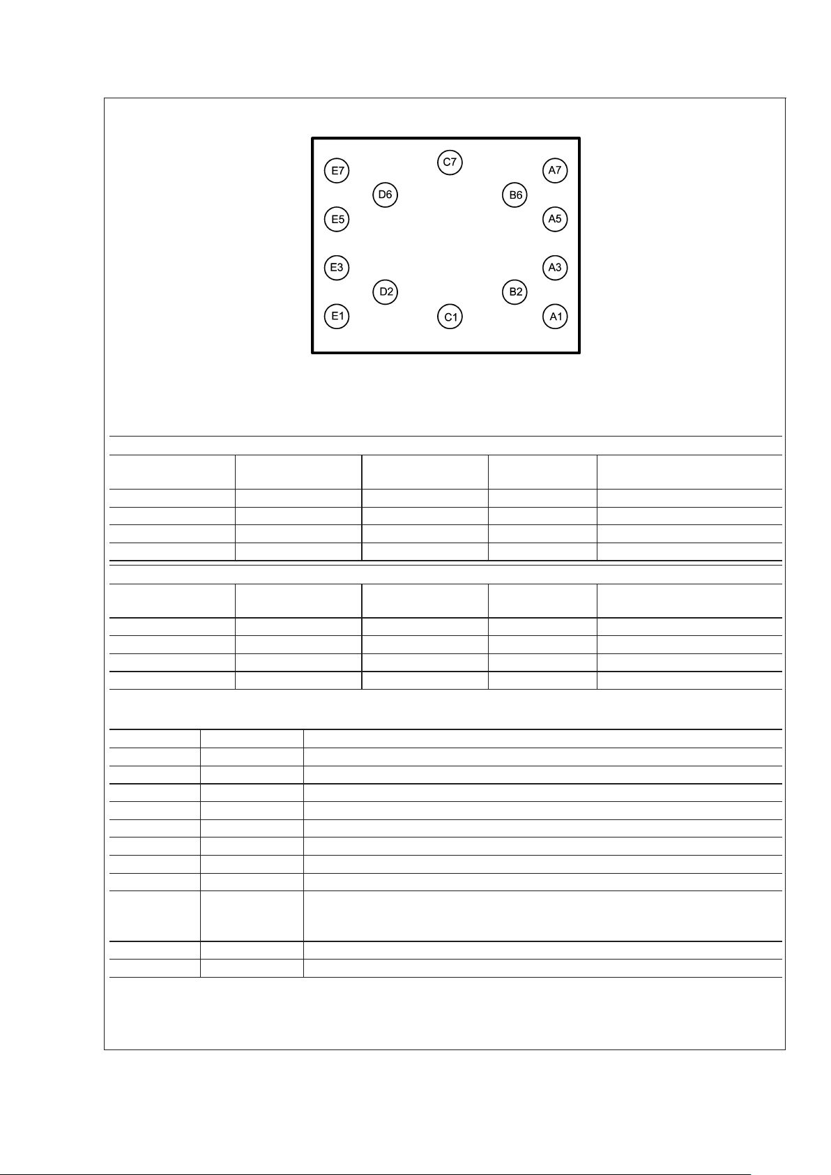
Connection Diagram
20028523
Bottom View
Ordering Information
Standard Micro SMD Package:
Order Number Shutdown Polarity Package Number Package
Marking
Supplied As
LM2794BL Active Low BLP14EHB I LOG 250 Units, Tape and Reel
LM2794BLX Active Low BLP14EHB I LOG 3000 Units, Tape and Reel
LM2795BL Active High BLP14EHB I LOJ 250 Units, Tape and Reel
LM2795BLX Active High BLP14EHB I LOJ 3000 Units, Tape and Reel
Thin Micro SMD Package:
Order Number Shutdown Polarity Package Number Package
Marking
Supplied As
LM2794TL Active Low TLP14EHA I LOG 250 Units, Tape and Reel
LM2794TLX Active Low TLP14EHA I LOG 3000 Units, Tape and Reel
LM2795TL Active High TLP14EHA I LOJ 250 Units, Tape and Reel
LM2795TLX Active High TLP14EHA I LOJ 3000 Units, Tape and Reel
Pin Description
Pin(*) Name Function
A1 C1+ Positive terminal of C1
B2 C1− Negative terminal of C1
C1 V
IN
Power supply voltage input
D2 GND Power supply ground input
E1 C2− Negative terminal of C2
E3,E5,E7,D6 D1−4 Current source outputs. Connect directly to LED
C7 I
SET
Current Sense Input. Connect 1% resistor to ground to set constant current through LED
B6 BRGT Variable voltage input controls output current
A7 SD The LM2794 has an active-low shutdown pin (LOW = shutdown, HIGH = operating). The
LM2795 has an active-high shutdown pin (HIGH = shutdown, LOW = operating) that has a
pull-up to V
IN
.
A5 C2+ Positive terminal of C2
A3 P
OUT
Charge pump output
(*) Note that the pin numbering scheme for the Micro SMD package was revised in April, 2002 to conform to JEDEC standard. Only the pin numbers were revised.
No changes to the physical location of the inputs/outputs were made. For reference purpose, the obsolete numbering had C1+ as pin 1, C1- as pin 2, VIN as pin
3, GND as pin 4, C2- as pin 5, D1-D4 as pin 6,7,8 & 9, Iset as pin 10, BRGT as pin 11, SD as pin 12, C2+ as pin 13, Pout as pin 14
LM2794/LM2795
www.national.com 2
Page 3
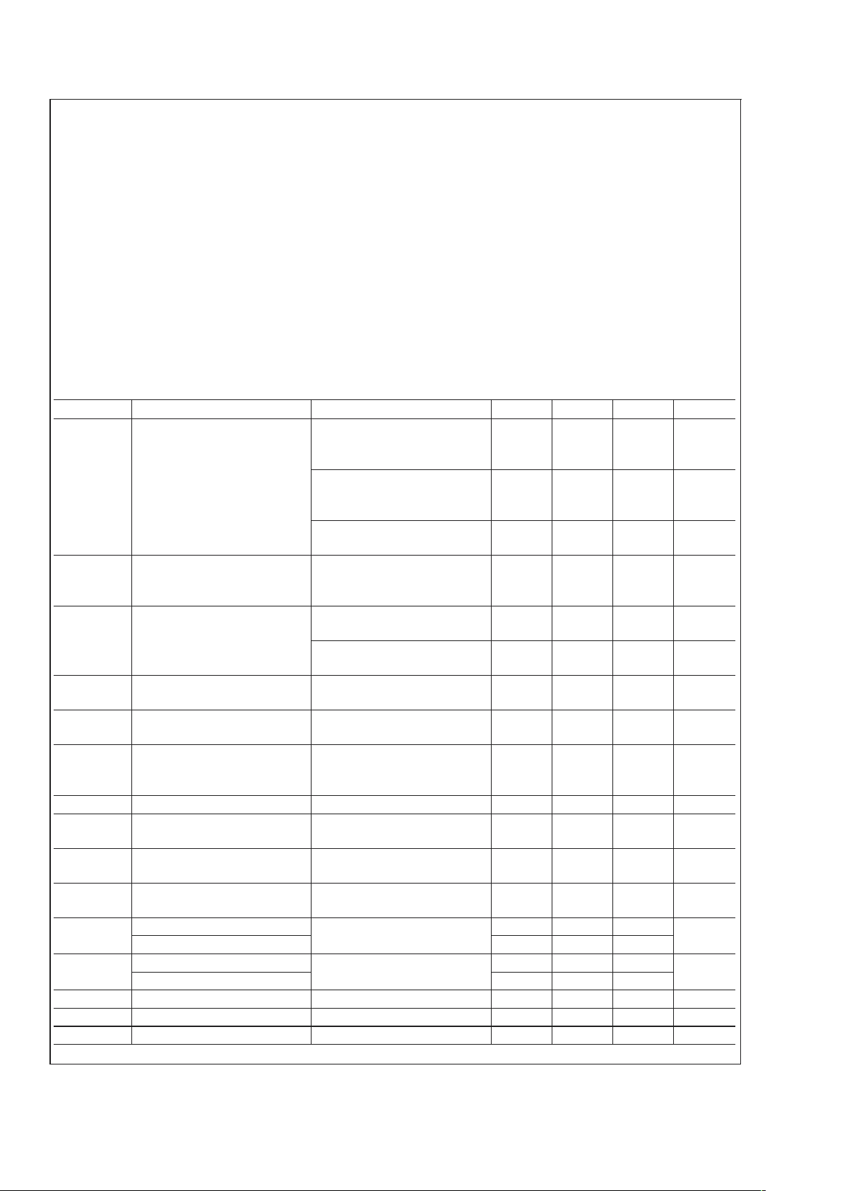
Absolute Maximum Ratings (Note 1)
If Military/Aerospace specified devices are required,
please contact the National Semiconductor Sales Office/
Distributors for availability and specifications.
V
IN
−0.5 to 6.2V max
SD −0.5 to (V
IN
+0.3V) w/
6.2V max
BRGT −0.5 to (V
IN
+0.3V) w/
6.2V max
Continuous Power Dissipation
(Note 2) Internally Limited
T
JMAX
(Note 2) 135˚C
θ
JA
(Notes 2, 3) 125˚C/W
Storge Temperature −65˚C to +150˚C
Lead Temp. (Soldering, 5 sec.) 260˚C
ESD Rating (Note 4)
Human Body Model 2kV
Machine Model 200V
Operating Conditions
Input Voltage (VIN) 2.7V to 5.5V
Ambient Temperature (T
A
) −30˚C to +85˚C
Junction Temperature (T
J
) −30˚C to +100˚C
Electrical Characteristics
Limits in standard typeface are for TJ= 25˚C and limits in boldface type apply over the full Operating Junction Temperature
Range (−30˚C ≤ T
J
≤ +100˚C). Unless otherwise specified, C1 = C2 = CIN=C
HOLD
= 1 µF, VIN= 3.6V, BRGT pin = 0V; R
SET
=124Ω ; LM2794:VSD=VIN(LM2795: VSD= 0V).
Symbol Parameter Conditions Min Typ Max Units
I
DX
Available Current at Output Dx 3.0V ≤ VIN≤ 5.5V
V
DX
≤ 3.8V
BRGT = 50mV
15 16.8 mA
2.7V ≤ V
IN
≤ 3.0V
V
DX
≤ 3.6V
BRGT = 0V
10
mA
V
DX
≤ 3.8V
BRGT = 200mV
20
mA
V
DX
Available Voltage at Output Dx 3.0V ≤ VIN≤ 5.5V
I
DX
≤ 15mA
BRGT = 50mV
3.8 V
I
DX
Line Regulation of Dx Output
Current
3.0V ≤ VIN≤ 5.5V
V
DX
= 3.6V
14.18 15.25 16.78 mA
3.0V ≤ V
IN
≤ 4.4V
V
DX
= 3.6V
14.18 15.25 16.32 mA
I
DX
Load Regulation of Dx Output
Current
VIN= 3.6V
3.0V ≤ V
DX
≤ 3.8V
14.18 15.25 16.32 mA
I
D-MATCH
Current Matching Between Any
Two Outputs
VIN= 3.6V, VDX= 3.6V 0.5 %
I
Q
Quiescent Supply Current 3.0V ≤ VIN≤ 4.2V, Active, No
Load Current
R
SET
= OPEN
5.5 8.2 mA
I
SD
Shutdown Supply Current 3.0V ≤ VIN≤ 5.5V, Shutdown 2.3 5 µA
I
PULL-SD
Shutdown Pull-Up Current
(LM2795)
VIN= 3.6V 1.5 µA
V
CP
Input Charge-Pump Mode To
Pass Mode Threshold
4.7 V
V
CPH
Input Charge-Pump Mode To
Pass Mode Hysteresis
(Note 5) 250 mV
V
IH
SD Input Logic High (LM2794) 3.0V ≤ VIN≤ 5.5V 1.0 V
SD Input Logic High (LM2795) 0.8V
IN
V
IL
SD Input Logic Low (LM2794) 3.0V ≤ VIN≤ 5.5V 0.2 V
SD Input Logic Low (LM2795) 0.2V
IN
I
LEAK-SD
SD Input Leakage Current 0V ≤ VSD≤ V
IN
100 nA
R
BRGT
BRGT Input Resistance 240 kΩ
I
SET
I
SET
Pin Output Current IDX/10 mA
LM2794/LM2795
www.national.com3
Page 4
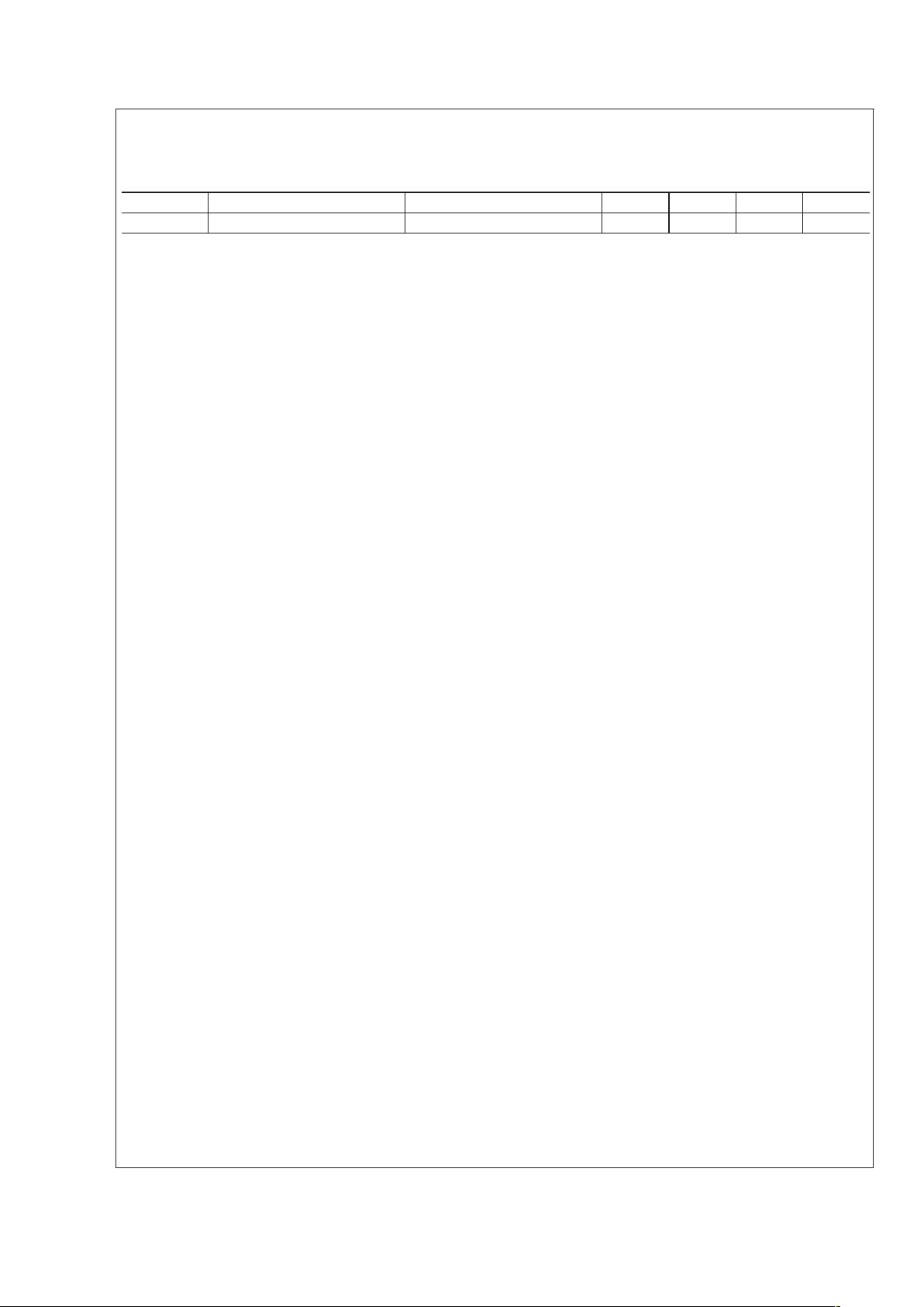
Electrical Characteristics (Continued)
Limits in standard typeface are for TJ= 25˚C and limits in boldface type apply over the full Operating Junction Temperature
Range (−30˚C ≤ T
J
≤ +100˚C). Unless otherwise specified, C1 = C2 = CIN=C
HOLD
= 1 µF, VIN= 3.6V, BRGT pin = 0V; R
SET
=124Ω ; LM2794:VSD=VIN(LM2795: VSD= 0V).
Symbol Parameter Conditions Min Typ Max Units
f
SW
Switching Frequency (Note 6) 3.0V ≤ VIN≤ 4.4V 325 515 675 kHz
Note 1: Absolute maximum ratings indicate limits beyond which damage to the device may occur. Electrical specifications do not apply when operating the device
beyond its rated operating conditions.
Note 2: Internal thermal shutdown circuitry protects the device from permanent damage. Thermal shutdown engages at T
J
=150˚C (typ.) and disengages at
T
J
=140˚C (typ.). D1, D2, D3 and D4 may be shorted to GND without damage. P
OUT
may be shorted to GND for 1sec without damage.
Note 3: The value of θ
JA
is based on a two layer evaluation board with a dimension of 2in. x1.5in.
Note 4: In the test circuit, all capacitors are 1.0µF, 0.3Ω maximum ESR capacitors. Capacitors with higher ESR will increase output resistance, reduce output
voltage and efficiency.
Note 5: Voltage at which the device switches from charge-pump mode to pass mode or pass mode to charge-pump mode. For example, during pass mode the
device output (Pout) follows the input voltage.
Note 6: The output switches operate at one eigth of the oscillator frequency, f
OSC
= 1/8fSW.
LM2794/LM2795
www.national.com 4
Page 5
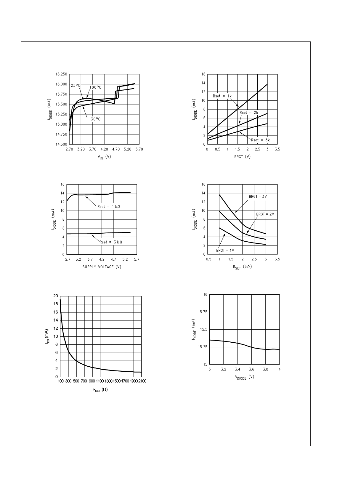
Typical Performance Characteristics Unless otherwise specified, C1 = C2 = C
IN=CHOLD
= 1µF,
V
IN
= 3.6V, BRGT pin = 0V, R
SET
= 124Ω.
I
DIODE
vs V
IN
I
DIODE
vs BRGT
20028512
20028509
I
DIODE
vs V
IN
BRGT = 3V I
DIODE
vs R
SET
20028507
20028508
I
DIODE
vs R
SET
V
BRGT
=0V I
DIODE
vs V
DIODE
20028541
20028524
LM2794/LM2795
www.national.com5
Page 6
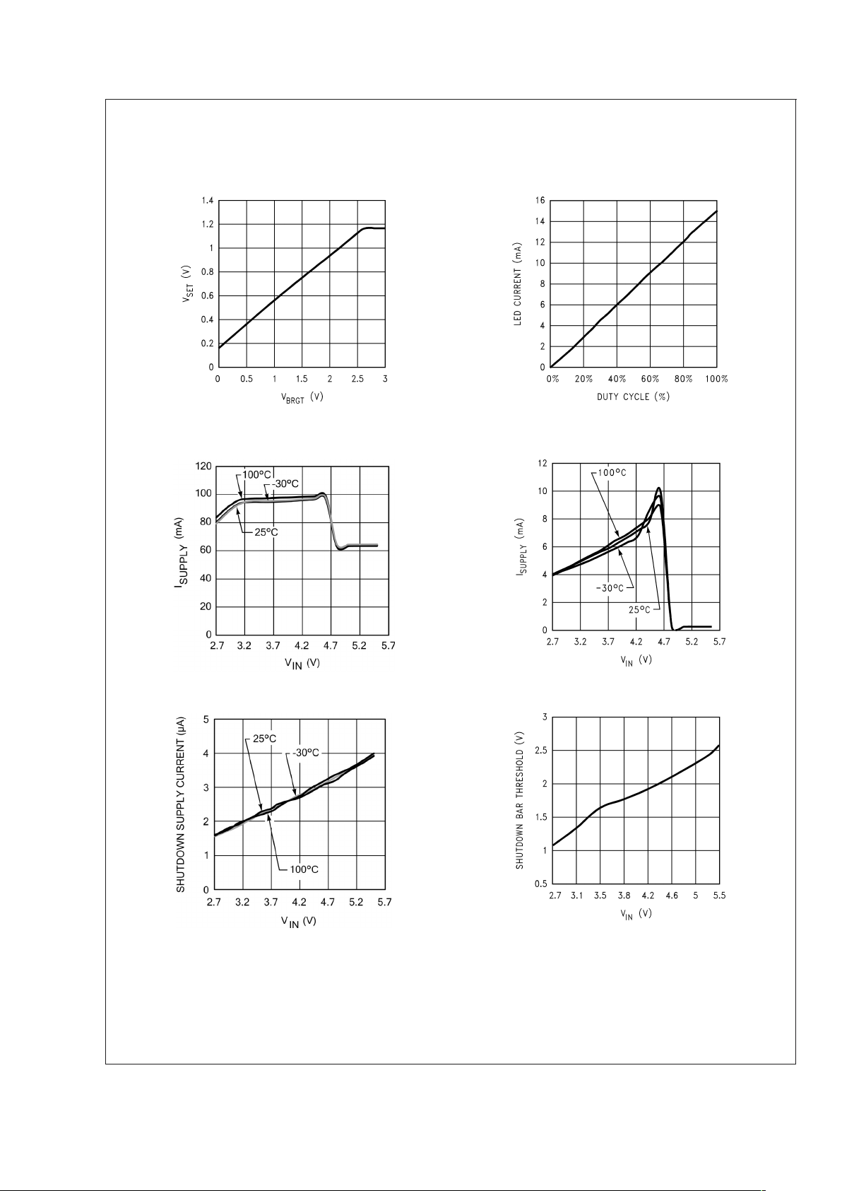
Typical Performance Characteristics Unless otherwise specified, C1 = C2 = C
IN=CHOLD
= 1µF, V
IN
= 3.6V, BRGT pin = 0V, R
SET
= 124Ω. (Continued)
V
SET
vs V
BRGT
R
SET
=1KΩ
Duty Cycle vs. Led Current (LM2794)
I
DIODE
1- 4 = 15mA
20028506
20028532
Supply Current vs V
IN
I
DIODE
1-4 = 15mA
Supply Current vs V
IN
I
DIODE
1-4 = Open
20028514
20028515
Shutdown Supply Current vs V
IN
Shutdown Threshold vs V
IN
20028513
20028505
LM2794/LM2795
www.national.com 6
Page 7

Typical Performance Characteristics Unless otherwise specified, C1 = C2 = C
IN=CHOLD
= 1µF, V
IN
= 3.6V, BRGT pin = 0V, R
SET
= 124Ω. (Continued)
Start-Up Response
@
VIN= 2.7V (LM2794) Start-Up Response@VIN= 2.7V (LM2795)
20028517 20028520
Start-Up Response@VIN= 3.6V (LM2794) Start-Up Response@VIN= 3.6V (LM2795)
20028518 20028522
Start-Up Response@VIN= 4.2V (LM2794) Start-Up Response@VIN= 4.2V (LM2795)
20028519 20028521
LM2794/LM2795
www.national.com7
Page 8

Typical Performance Characteristics Unless otherwise specified, C1 = C2 = C
IN=CHOLD
= 1µF, V
IN
= 3.6V, BRGT pin = 0V, R
SET
= 124Ω. (Continued)
Available Additional Current
@
P
OUT
I
DIODE
1− 4 = 15mA, R
SET
= 124 Ω Switching Frequency
20028531
20028516
LM2794/LM2795
www.national.com 8
Page 9

Functional Block Diagram
20028530
LM2794/LM2795
www.national.com9
Page 10

Application Information
CIRCUIT DESCRIPTION
The LM2794/5 is a 1.5x/1x CMOS charge pump with four
matched constant current outputs, each capable of driving
up to 20mA through White LEDs. This device operates over
the extended Li-Ion battery range from 2.7V to 5.5V. The
LM2794/5 has four regulated current sources connected to
the device’s 1.5x charge pump output (P
OUT
). At input voltages below 4.7V (typ.), the charge-pump provides the
needed voltage to drive high forward voltage drop White
LEDs. It does this by stepping up the P
OUT
voltage 1.5 times
the input voltage. The charge pump operates in Pass Mode,
providing a voltage on P
OUT
equal to the input voltage, when
the input voltage is at or above 4.7V (typ.). The device can
drive up to 80mA through any combination of LEDs connected to the constant current outputs D
1-D4
.
To set the LED drive current, the device uses a resistor
connected to the I
SET
pin to set a reference current. This
reference current is then multiplied and mirrored to each
constant current output. The LED brightness can then be
controlled by analog and/or digital methods. Applying an
analog voltage in the range of 0V to 3.0V to the Brightness
pin (BRGT) adjusts the dimming profile of the LEDs. The
digital technique uses a PWM (Pulse Width Modulation)
signal applied to the Shutdown pin (SD). (see I
SET
and
BRGT PINS section).
SOFT START
Soft start is implemented internally by ramping the reference
voltage more slowly than the applied voltage. During soft
start, the current through the LED outputs will ramp up in
proportion to the rate that the reference voltage is being
ramped up.
SHUTDOWN MODE
The shutdown pin (SD) disables the part and reduces the
quiescent current to 2.3µA (typ.).
The LM2795 has an active-high shutdown pin (HIGH =
shutdown, LOW = operating). An internal pull-up is connected between SD and V
IN
of the LM2795. This allows the
use of open-drain logic control of the LM2795 shutdown, as
shown in Figure 1. The LM2795 SD pin can also be driven
with a rail-to-rail CMOS logic signal.
The LM2794 has an active-low shutdown pin (LOW = shutdown, HIGH = operating). The LM2794 SD pin can be driven
with a low-voltage CMOS logic signal (1.5V logic, 1.8V logic,
etc). There is no internal pull-up or pull-down on the SD pin
of the LM2794.
CAPACITOR SELECTION
The LM2794/5 requires 4 external capacitors for proper
operation. Surface-mount multi-layer ceramic capacitors are
recommended. These capacitors are small, inexpensive and
have very low equivalent series resistance (ESR, ≤15mΩ
typ.). Tantalum capacitors, OS-CON capacitors, and aluminum electrolytic capacitors are generally not recommended
for use with the LM2794/5 due to their high ESR, as compared to ceramic capacitors.
For most applications, ceramic capacitors with X7R or X5R
temperature characteristic are preferred for use with the
LM2794/5. These capacitors have tight capacitance tolerance (as good as
±
10%), hold their value over temperature
(X7R:
±
15% over −55˚C to 125˚C; X5R:±15% over −55˚C
to 85˚C), and typically have little voltage coefficient. Capacitors with Y5V or Z5U temperature characteristic are generally not recommended for use with the LM2794/5. Capacitors with these temperature characteristics typically have
wide capacitance tolerance (+80%, −20%), vary significantly
over temperature (Y5V: +22%, −82% over −30˚C to +85˚C
range; Z5U: +22%, −56% over +10˚C to +85˚C range), and
have poor voltage coefficients. Under some conditions, a
nominal 1µF Y5V or Z5U capacitor could have a capacitance
of only 0.1µF. Such detrimental deviation is likely to cause
Y5V and Z5U capacitors to fail to meet the minimum capacitance requirements of the LM2794/5. Table 1 lists suggested
capacitor suppliers for the typical application circuit.
TABLE 1. Ceramic Capacitor Manufacturers
Manufacturer Contact
TDK www.component.tdk.com
Murata www.murata.com
Taiyo Yuden www.t-yuden.com
LED SELECTION
The LM2794/5 is designed to drive LEDs with a forward
voltage of about 3.0V to 4.0V. The typical and maximum
diode forward voltage depends highly on the manufacturer
and their technology. Table 2 lists two suggested manufacturers. Forward current matching is assured over the LED
process variations due to the constant current output of the
LM2794/5.
TABLE 2. White LED Selection
Manufacturer Contact
Osram www.osram-os.com
Nichia www.nichia.com
I
SET
AND BRGT PINS
An external resistor, R
SET
, is connected to the I
SET
pin to set
the current to be mirrored in each of the LED outputs. The
internal current mirror sets each LED output current with a
10:1 ratio to the current through R
SET
. The current mirror
circuitry matches the current through each LED to within
0.5%.
In addition to R
SET
, a voltage may be applied to the V
BRGT
pin to vary the LED current. By adjusting current with the
Brightness pin (BRGT), the brightness of the LEDs can be
smoothly varied.
20028536
FIGURE 1. Open-Drain Logic Shutdown Control
LM2794/LM2795
www.national.com 10
Page 11

Application Information (Continued)
Applying a voltage on BRGT between 0 to 3 volts will linearly
vary the LED current. Voltages above 3V do not increase the
LED current any further. The voltage on the V
BRGT
pin is fed
into an internal resistor network with a ratio of 0.385. The
resulting voltage is then summed with a measured offset
voltage of 0.188V, which comes from the reference voltage
being fed through a resistor network (See Functional Block
Diagram). The brightness control circuitry then uses the
summed voltage to control the voltage across R
SET
.An
equation for approximating the LED current is:
20028540
I
LED
CURRENT SELECTION PROCEDURES
The following procedures illustrate how to set and adjust
output current levels. For constant brightness or analog
brightness control, go to “Brightness control using BRGT”.
Otherwise refer to “Brightness control using PWM”.
Brightness Control Using PWM
1. Set the BRGT pin to 0V.
2. Determine the maximum desired I
LED
current. Use the
I
LED
equation to calculate R
SET
by setting BRGT to 0V or
use Table 3 to select a value for R
SET
when BRGT
equals 0V.
3. Brightness control can be implemented by pulsing a
signal at the SD pin. LED brightness is proportional to
the duty cycle (D) of the PWM signal. For linear brightness control over the full duty cycle adjustment range,
the PWM frequency (f) should be limited to accommodate the turn-on time (T
ON
= 100µs) of the device.
D x (1/f)
>
T
ON
f
MAX=DMIN÷TON
If the PWM frequency is much less than 100Hz, flicker
may be seen in the LEDs. For the LM2794, zero duty
cycle will turn off the LEDs and a 50% duty cycle will
result in an average I
LED
being half of the programmed
LED current. For example, if R
SET
is set to program
15mA, a 50% duty cycle will result in an average I
LED
of
7.5mA. For the LM2795 however, 100% duty cycle will
turn off the LEDs and a 50% duty cycle will result in an
average I
LED
being half the programmed LED current.
Brightness Control Using BRGT
1. Choose the maximum I
LED
desired and determine the
max voltage to be applied to the BRGT pin. For constant
brightness, set BRGT to a fixed voltage between 0V to
3V.
2. Use Table 3 to determine the value of R
SET
required or
use the I
LED
equation above to calculate R
SET
.
3. Use Table 4 as a reference for the dimming profile of the
LEDs, when BRGT ranges from 0V to 3V.
TABLE 3. R
SET
Values
LED Current
BRGT 5mA 10mA 15mA 20mA
0.0V 374Ω 187Ω 124Ω 93.1Ω
0.5V 768Ω 383Ω 255Ω 191Ω
1.0V 1.15KΩ 576Ω 383Ω 287Ω
1.5V 1.54KΩ 768Ω 511Ω 383Ω
2.0V 1.91KΩ 953Ω 624Ω 475Ω
2.5V 2.32KΩ 1.15KΩ 768Ω 576Ω
3.0V 2.67KΩ 1.33KΩ 909Ω 665Ω
R
SET
values are rounded off to the nearest 1% standard values.
TABLE 4. LED Current
R
SET
Values
BRGT 2.67KΩ 1.33KΩ 909Ω 665Ω
0.0V 0.7mA 1.4mA 2.1mA 2.8mA
0.5V 1.4mA 2.9mA 4.2mA 5.7mA
1.0V 2.1mA 4.3mA 6.3mA 8.6mA
1.5V 2.9mA 5.8mA 8.4mA 11.5mA
2.0V 3.6mA 7.2mA 10.5mA 14.4mA
2.5V 4.3mA 8.7mA 12.7mA 17.3mA
3.0V 5.0mA 10.1mA 14.8mA 20.2mA
CHARGE PUMP OUTPUT (P
OUT
)
The LM2794/5 charge pump is an unregulated switched
capacitor converter with a gain of 1.5. The voltage at the
output of the pump (the P
OUT
pin) is nominally 1.5 x VIN. This
rail can be used to deliver additional current to other circuitry.
Figure 2 shows how to connect additional LEDs to P
OUT
.A
ballast resistor sets the current through each LED, and LED
current matching is dependent on the LED forward voltage
matching. Because of this, LEDs driven by P
OUT
are recommended for functions where brightness matching is not critical, such as keypad backlighting.
Since P
OUT
is unregulated, driving LEDs directly off P
OUT
is
usually practical only with a fixed input voltage. If the input
voltage is not fixed (Li-Ion battery, for example), using a
linear regulator between the P
OUT
pin and the LEDs is
recommended. National Semiconductor’s LP3985-4.5V lowdropout linear regulator is a good choice for such an application.
The voltage at P
OUT
is dependent on the input voltage
supplied to the LM2794/5, the total LM2794/5 output current,
and the output resistance (R
OUT
) of the LM2794/5 charge
pump. Output resistance is a model of the switching losses
of the charge pump. Resistances of the internal charge
pump switches (MOS transistors) are a primary component
of the LM2794/5 output resistance. Typical LM2794/5 output
resistance is 3.0Ω. For worst-case design calculations, using
an output resistance of 3.5Ω is recommended. (Worst-case
recommendation accounts for parameter shifts from part-topart variation and applies over the full operating temperature
range).
LM2794/LM2795
www.national.com11
Page 12

Application Information (Continued)
20028535
FIGURE 2. Keypad LEDs Connected to P
OUT
LM2794/LM2795
www.national.com 12
Page 13

Application Information (Continued)
Output resistance results in droop in the P
OUT
voltage proportional to the amount of current delivered by the pump.
The P
OUT
voltage is an important factor in determining the
total output current capability of an application. Taking total
output current to be the sum of all D
X
output currents plus
the current delivered through the P
OUT
pin, the voltage at
P
OUT
can be predicted with the following equations:
I
TOTAL=ID1+ID2+ID3+ID4+IPOUT
V
POUT
=1.5xVIN−I
TOTALxROUT
LED HEADROOM VOLTAGE (VHR)
Four current sources are connected internally between P
OUT
and D1-D4. The voltage across each current source, (V
POUT
−VDX), is referred to as headroom voltage (VHR). The current sources require a sufficient amount of headroom voltage
to be present across them in order to regulate properly.
Minimum required headroom voltage is proportional to the
current flowing through the current source, as dictated by the
equation:
V
HR-MIN=kHRxIDX
The parameter kHR, typically 20mV/mA in the LM2794/5, is a
proportionality constant that represents the ON-resistance of
the internal current mirror transistors. For worst-case design
calculations, using a k
HR
of 25mV/mA is recommended.
(Worst-case recommendation accounts for parameter shifts
from part-to-part variation and applies over the full operating
temperature range). Figure 3 shows how output current of
the LM2794/5 varies with respect to headroom voltage.
On the flat part of the graph, the currents regulate properly
as there is sufficient headroom voltage for regulation. On the
sloping part of the graph the headroom voltage is too small,
the current sources are squeezed, and their current drive
capability is limited. Changes in headroom voltage from one
output to the next, possible with LED forward voltage mismatch, will result in different output currents and LED brightness mismatch. Thus, operating the LM2794/5 with insufficient headroom voltage across the current sources should
be avoided.
OUTPUT CURRENT CAPABILITY
The primary constraint on the total current capability is the
headroom voltage requirement of the internal current
sources. Combining the V
POUT
and VHRequations from the
previous two sections yields the basic inequality for determining the validity of an LM2794/5 LED-drive application:
V
POUT
=1.5xVIN−I
TOTALxROUT
V
HR-MIN=kHRxIDX
V
POUT−VDX
≥ V
HR-MIN
1.5xVIN−I
TOTALxROUT−VDX
≥ (kHRxIDX)
Rearranging this inequality shows the estimated total output
current capability of an application:
I
TOTAL
≤ [(1.5 x V
IN-MIN
)−V
DX-MAX
−(kHRxIDX)]÷R
OUT
Examining the equation above, the primary limiting factors
on total output current capability are input and LED forward
voltage. A low input voltage combined with a high LED
voltage may result in insufficient headroom voltage across
the current sources, causing them to fall out of regulation.
When the current sources are not regulated, LED currents
will be below desired levels and brightness matching will be
highly dependent on LED forward voltage matching.
Typical LM2794/5 output resistance is 3.0Ω. For worst-case
design calculations, using an output resistance of 3.5Ω is
recommended. LM2794/5 has a typical k
HR
constant of
20mV/mA. For worst-case design calculations, use k
HR
=
25mV/mA. (Worst-case recommendations account for parameter shifts from part-to-part variation and apply over the
full operating temperature range). R
OUT
and kHRincrease
slightly with temperature, but losses are typically offset by
the negative temperature coefficient properties of LED forward voltages. Power dissipation and internal self-heating
may also limit output current capability but is discussed in a
later section.
PARALLEL Dx OUTPUTS FOR INCREASED CURRENT
DRIVE
Outputs D
1
through D4may be connected together in any
combination to drive higher currents through fewer LEDs.
For example in Figure 4, outputs D
1
and D2are connected
together to drive one LED while D
3
and D4are connected
together to drive a second LED.
20028539
FIGURE 3. I
LED
vs V
HR
4 LEDs, VIN= 3.0V
20028533
FIGURE 4. Two Parallel Connected LEDs
LM2794/LM2795
www.national.com13
Page 14

Application Information (Continued)
With this configuration, two parallel current sources of equal
value provide current to each LED. R
SET
and V
BRGT
should
therefore be chosen so that the current through each output
is programmed to 50% of the desired current through the
parallel connected LEDs. For example, if 30mA is the desired drive current for 2 parallel connected LEDs , R
SET
and
V
BRGT
should be selected so that the current through each of
the outputs is 15mA. Other combinations of parallel outputs
may be implemented in similar fashions, such as in Figure 5.
Connecting outputs in parallel does not affect internal operation of the LM2794/95 and has no impact on the Electrical
Characteristics and limits previously presented. The available diode output current, maximum diode voltage, and all
other specifications provided in the Electrical Characteristics
table apply to parallel output configurations, just as they do
to the standard 4-LED application circuit.
THERMAL PROTECTION
When the junction temperature exceeds 150˚C (typ.), the
LM2794/5 internal thermal protection circuitry disables the
part. This feature protects the device from damage due to
excessive power dissipation. The device will recover and
operate normally when the junction temperature falls below
140˚C (typ.). It is important to have good thermal conduction
with a proper layout to reduce thermal resistance.
POWER EFFICIENCY
Figure 6 shows the efficiency of the LM2794/5. The change
in efficiency shown by the graph comes from the transition
from Pass Mode to a gain of 1.5.
Efficiency (E) of the LM2794/5 is defined here as the ratio of
the power consumed by LEDs (P
LED
) to the power drawn
from the input source (P
IN
). In the equations below, IQis the
quiescent current of the LM2794/5, I
LED
is the current flowing
through one LED, V
LED
is the forward voltage at that LED
current, and N is the number of LEDs connected to the
regulated current outputs. In the input power calculation, the
1.5 represents the switched capacitor gain configuration of
the LM2794/5.
P
LED
=NxV
LEDxILED
PIN=VINxI
IN
PIN=VINx(1.5xNxI
LED+IQ
)
E=(P
LED÷PIN
)
Efficiency, as defined here, is in part dependent on LED
voltage. Variation in LED voltage does not affect power
consumed by the circuit and typically does not relate to the
brightness of the LED. For an advanced analysis, it is recommended that power consumed by the circuit (V
INxIIN
)be
evaluated rather than power efficiency. Figure 7 shows the
power consumption of the LM2794/5 Typical Application Circuit.
20028534
FIGURE 5. One Parallel Connected LED
20028537
FIGURE 6. Efficiency vs V
IN
4 LEDs, V
LED
= 3.6V, I
LED
= 15mA
LM2794/LM2795
www.national.com 14
Page 15

Application Information (Continued)
POWER DISSIPATION
The power dissipation (P
DISSIPATION
) and junction tempera-
ture (T
J
) can be approximated with the equations below. P
IN
is the power generated by the 1.5x charge pump, P
LED
is the
power consumed by the LEDs, P
POUT
is the power provided
through the P
OUT
pin, TAis the ambient temperature, and θ
JA
is the junction-to-ambient thermal resistance for the micro
SMD-14 package. V
IN
is the input voltage to the LM2794/5,
V
DX
is the LED forward voltage, IDXis the programmed LED
current, and I
POUT
is the current drawn through P
OUT
.
P
DISSIPATION=PIN-PLED−PPOUT
= [1.5xVINx(4IDX+I
POUT
)]−(VDXx4IDX) − (1.5xVINxI
POUT
)
T
J=TA
+(P
DISSIPATION
x θJA)
The junction temperature rating takes precedence over the
ambient temperature rating. The LM2794/5 may be operated
outside the ambient temperature rating, so long as the junction temperature of the device does not exceed the maximum operating rating of 100˚C. The maximum ambient temperature rating must be derated in applications where high
power dissipation and/or poor thermal resistance causes the
junction temperature to exceed 100˚C.
MICRO SMD MOUNTING
The LM2794/5 is a 14-bump micro SMD with a bump size of
300 micron diameter. The micro SMD package requires
specific mounting techniques detailed in National Semiconductor Application Note (AN -1112). NSMD (non-solder mask
defined) layout pattern is recommended over the SMD (solder mask defined) since the NSMD requires larger solder
mask openings over the pad size as opposed to the SMD.
This reduces stress on the PCB and prevents possible
cracking at the solder joint. For best results during assembly,
alignment ordinals on the PC board should be used to
facilitate placement of the micro SMD device. Micro SMD is
a wafer level chip size package, which means the dimensions of the package are equal to the die size. As such, the
micro SMD package lacks the plastic encapsulation characteristics of the larger devices and is sensitive to direct exposure to light sources such as infrared, halogen, and sun light.
The wavelengths of these light sources may cause unpredictable operation.
20028538
FIGURE 7. PINvs V
IN
4 LEDs, 2.5 ≤ VDX≤ 3.9V, IDX= 15mA
LM2794/LM2795
www.national.com15
Page 16

Physical Dimensions inches (millimeters) unless otherwise noted
Standard Micro SMD Package
For Ordering, Refer to Ordering Information Table
NS Package Number BLP14
The dimensions for X1, X2, X3 are given as:
X1 = 2.08mm
±
0.03mm
X2 = 2.403mm
±
0.03mm
X3 = 0.845mm
±
0.01mm
LM2794/LM2795
www.national.com 16
Page 17

Physical Dimensions inches (millimeters) unless otherwise noted (Continued)
Thin Micro SMD Package
For Ordering, Refer to Ordering Information Table
NS Package Number TLP14
The dimensions for X1, X2, X3 are given as:
X1 = 2.08mm
±
0.03mm
X2 = 2.403mm
±
0.03mm
X3 = 0.600mm
±
0.075mm
LIFE SUPPORT POLICY
NATIONAL’S PRODUCTS ARE NOT AUTHORIZED FOR USE AS CRITICAL COMPONENTS IN LIFE SUPPORT
DEVICES OR SYSTEMS WITHOUT THE EXPRESS WRITTEN APPROVAL OF THE PRESIDENT AND GENERAL
COUNSEL OF NATIONAL SEMICONDUCTOR CORPORATION. As used herein:
1. Life support devices or systems are devices or
systems which, (a) are intended for surgical implant
into the body, or (b) support or sustain life, and
whose failure to perform when properly used in
accordance with instructions for use provided in the
labeling, can be reasonably expected to result in a
significant injury to the user.
2. A critical component is any component of a life
support device or system whose failure to perform
can be reasonably expected to cause the failure of
the life support device or system, or to affect its
safety or effectiveness.
National Semiconductor
Americas Customer
Support Center
Email: new.feedback@nsc.com
Tel: 1-800-272-9959
National Semiconductor
Europe Customer Support Center
Fax: +49 (0) 180-530 85 86
Email: europe.support@nsc.com
Deutsch Tel: +49 (0) 69 9508 6208
English Tel: +44 (0) 870 24 0 2171
Français Tel: +33 (0) 1 41 91 8790
National Semiconductor
Asia Pacific Customer
Support Center
Email: ap.support@nsc.com
National Semiconductor
Japan Customer Support Center
Fax: 81-3-5639-7507
Email: jpn.feedback@nsc.com
Tel: 81-3-5639-7560
www.national.com
LM2794/LM2795 Current Regulated Switched Capacitor LED Supply with Analog and PWM
Brightness Control
National does not assume any responsibility for use of any circuitry described, no circuit patent licenses are implied and National reserves the right at any time without notice to change said circuitry and specifications.
 Loading...