

Page 1
December 2002
LM2760
3.3V Regulated Switched Capacitor Voltage Converter
LM2760 3.3V Regulated Switched Capacitor Voltage Converter
General Description
The LM2760 is a switched-capacitor DC/DC converter that
generates a regulated 3.3V output capable of driving a load
up to 20mA (V
(2.0V-4.4V) allows this device to be powered from several
types of batteries, including single cell lithium-ion, two-cell
alkaline, nickel-metal-hydride, and nickel-cadmium. The
LM2760 solution does not require an inductor and needs
only three small external ceramic capacitors. The miniscule
quiescent current of the part, typically 10µA unloaded,
makes the LM2760 ideal for low-current standby power rails.
The LM2760 is a switched-capacitor circuit that is controlled
by a gated oscillator. Both a low-input-voltage boost mode
and high-input-voltage pass mode are implemented to optimize efficiency over the full input voltage range.
Additional features of the LM2760 include thermal protection
and current limiting. The LM2760 is available in a small,
five-pin SOT-23 package.
≥ 2.5V). The wide input voltage range
IN
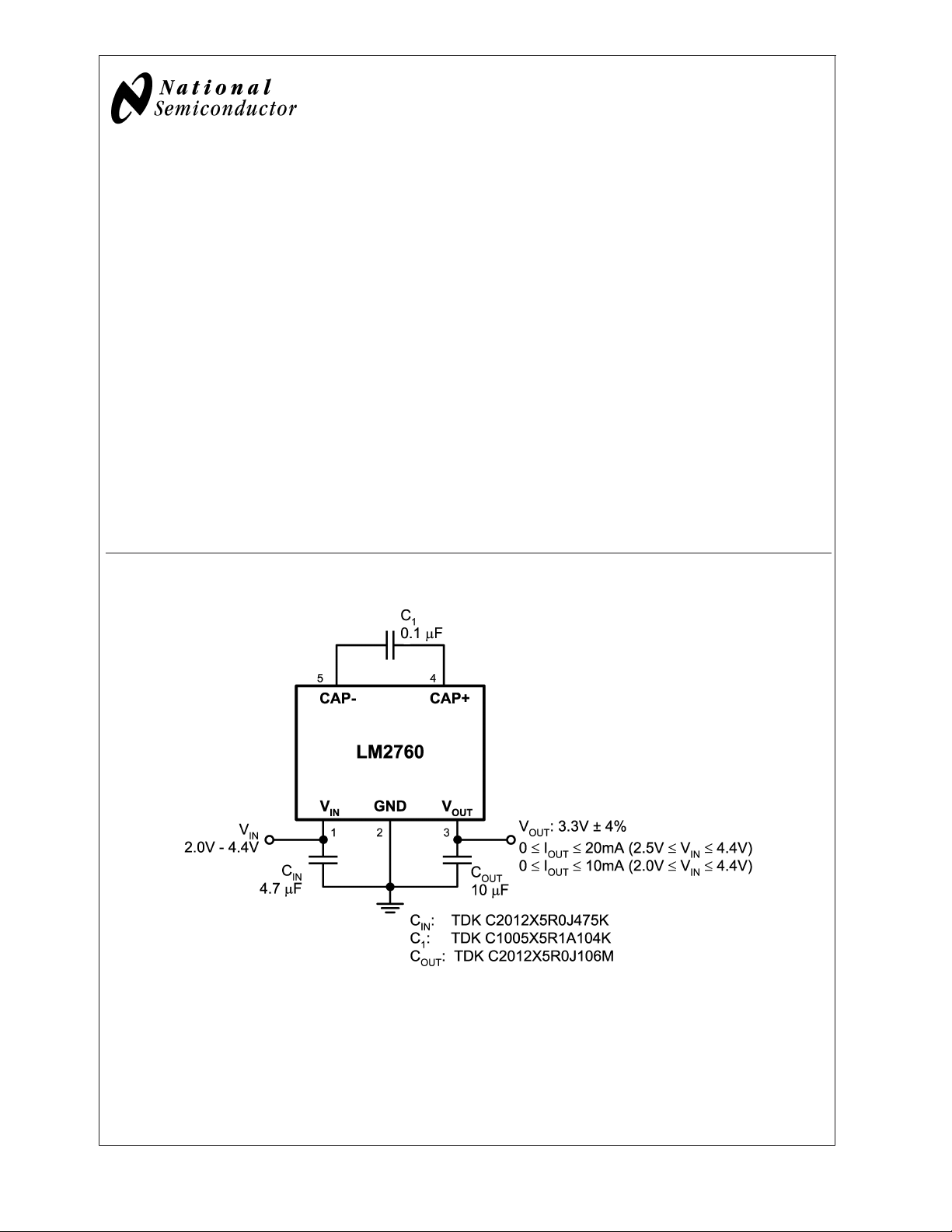
Typical Application Circuit
Features
n 3.3V±4% Regulated Output
n Ultralow Power: 10µA Typical Supply Current
n Boost and Pass Modes for Improved Efficiency
n Input Voltage Range: 2.0V to 4.4V
n Output Current up to 20mA (V
n Output Current up to 10mA (V
n Inductorless solution
n Small external parts count: 3 ceramic capacitors
n 750kHz Switching Frequency
n SOT23-5 Package
n Short-Circuit and Thermal Protection
≥ 2.5V)
IN
≥ 2.0V)
IN
Applications
n Battery-Operated Devices
n Cellular Phone
n Standby Power Supply
n Memory Keep-alive Power
20044301
© 2002 National Semiconductor Corporation DS200443 www.national.com
Page 2
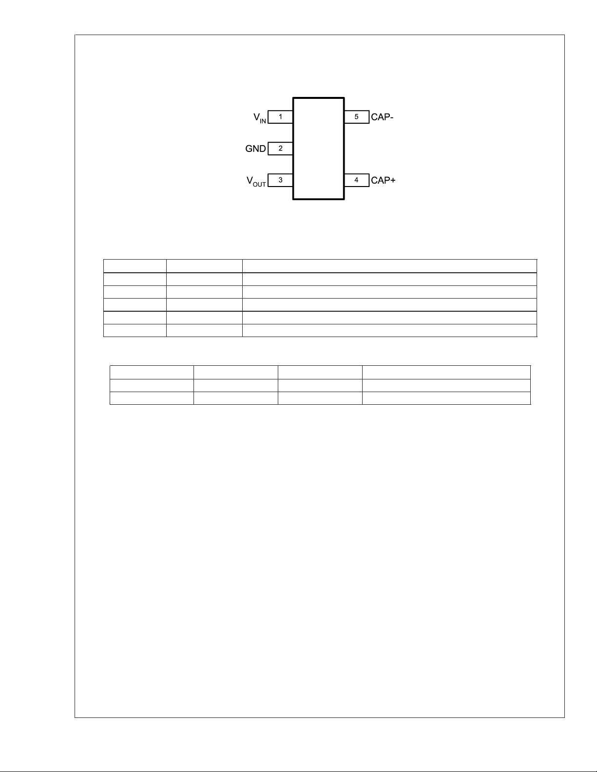
Connection Diagram
LM2760
LM2760
SOT23-5 Package
NS Package Number MF05A
Pin Description
Pin #(s) Pin Name Description
1V
2 GND Ground connection
3V
4 CAP+ Charge pump capacitor (+) connection
5 CAP- Charge pump capacitor (-) connnection
IN
OUT
Ordering Information
Order # Package Type Package Marking Supplied as
LM2760M5 SOT23-5 S19B Rail (250 units/rail)
LM2760M5X SOT23-5 S19B Tape and reel (3000 units/reel)
Top View
20044302
Input supply connection
Regulated 3.3V output
www.national.com 2
Page 3
LM2760
Absolute Maximum Ratings (Notes 1,
2)
If Military/Aerospace specified devices are required,
please contact the National Semiconductor Sales Office/
Distributors for availability and specifications.
Pin: Voltage to GND −0.3V to 6V
V
IN
Junction Temperature (T
J-MAX-ABS
Continuous Power Dissipation Internally Limited
) 150˚C
Operating Ratings (Notes 1, 2)
Input Voltage Range 2.0V to 4.4V
Recommended Output Current
2.5V ≤ V
2.0V ≤ V
Junction Temperature (T
Ambient Temperature (T
(Note 6)
≤ 4.4V 0mA to 20mA
IN
≤ 2.5V 0mA to 10mA
IN
) Range -40˚C to 100˚C
J
) Range
A
-40˚C to 85˚C
(Note 3)
V
Short-Circuit to GND Duration Unlimited
OUT
(Note 4)
Thermal Information
Storage Temperature Range -65˚C to 150˚C
Lead Temperature 260˚C
(Soldering, 5 sec.)
ESD Rating (Note 5)
Human-body model:
Machine model
2kV
200 V
Junction-to-Ambient Thermal 220˚C/W
Resistance (θ
), SOT23-5
JA
Package(Note 7)
Electrical Characteristics (Notes 2, 8)
Typical values and limits in standard typeface apply for TJ=25oC. Limits in boldface type apply over the operating junction
temperature range 0
= 10µF(Note 10)
C
OUT
Symbol Parameter Conditions Min Typ Max Units
V
OUT
I
Q
I
IN
f
OSC
V
p-p
t
ON
I
SC
Note 1: Absolute Maximum Ratings indicate limits beyond which damage to the component may occur. Operating Ratings are conditions under which operation of
the device is guaranteed. Operating Ratings do not imply guaranteed performance limits. For guaranteed performance limits and associated test conditions, see the
Electrical Characteristics tables.
Note 2: All voltages are with respect to the potential at the GND pin.
Note 3: Thermal shutdown circuitry protects the device from permanent damage.
Note 4: Excessive power dissipation will occur if the part is shorted to ground. Internal thermal shutdown will protect the device from permanent damage, but
thermal cycling of the part is likely to occur until the short is removed. Protection is guaranteed only for V
Note 5: : The human-body model is a 100 pF capacitor discharged through a 1.5 kΩ resistor into each pin. The machine model is a 200pF capacitor discharged
directly into each pin.
Note 6: Maximum ambient temperature (T
dissipation of the device in the application (P
following equation: T
LM2760 is 70mW. This occurs when the output current is 20mA and the input voltage is 3.4V (edge of the "doubler" region). The maximum ambient temperature
operating rating (T
Dissipation section of this datasheet.
Note 7: Junction-to-ambient thermal resistance (θ
guidelines set forth in the JEDEC standard JESD51-3. The test board is a 2-layer FR-4 board measuring 230mm x 125mm x 1.6mm. Thickness of the copper layers
is 18mm (1.0oz). Ambient temperature in simulation is 22˚C, still air. Power dissipation is 1W. Junction-to-ambient thermal resistance is a highly application-specific
parameter. The value of θ
Note 8: : All room temperature limits are 100% tested or guaranteed through statistical analysis. All limits at temperature extremes are guaranteed by correlation
using standard Statistical Quality Control methods (SQC). All limits are used to calculate Average Outgoing Quality Level (AOQL). Typical numbers are not
guaranteed, but do represent the most likely norm.
Note 9: With P
o
the 0
Note 10: C
D-MAX
C-to-85oC junction temperature range that is used in determining guaranteed limits.
FLY,CIN
o
C≤ TJ≤ +85oC[0oC ≤ TA≤ +70oC (Note 9)] Unless otherwise specified: CIN= 4.7µF, C
Output Voltage 2.5V ≤ VIN≤ 4.4V,
OUT
IN
OUT
≤ 20mA
≤ 4.4V,
≤ 10mA
0mA ≤ I
2.0V ≤ V
0mA ≤ I
Quiescent Supply Current 2.0V ≤ VIN≤ 4.4V, V
OUT
tied to
3.17 3.3 3.43 V
3.17 3.3 3.43 V
6 12 µA
FLY
= 0.1µF,
3.5V, unloaded (Note 11)
Normal Operation Supply
Current
2.0V ≤ VIN≤ 4.4V, unloaded,
Time-averaged (Note 12)
10 µA
Oscillator Frequency VIN= 3.0V 750 kHz
Output Ripple Voltage VIN= 3.0V, I
V
Turn-On Time VIN= 3.0V (Note 13) 1 ms
OUT
= 10mA 60 mV
OUT
Output Short Circuit Current VIN= 3.0V 170 mA
≤ 4.4V
IN
) is dependent on the maximum operating junction temperature (T
A-MAX
), and the junction-to-ambient thermal resistance of the part/package in the application (θJA), as given by the
D-MAX
A-MAX=TJ-MAX-OP
)of85oC is calculated using θJA= 220oC/W and P
A-MAX
of the LM2760 could fall in a range as wide as 150oC/W to 250oC/W (if not wider), depending on PCB and application conditions.
JA
of 70mW and θJAof 220oC/W (see Note 6), the ambient temperature range of 0oC-to-70oC is provided for convenience and is calculated from
, and C
OUT
-(θJAxP
: Low-ESR Surface-Mount Ceramic Capacitors (MLCCs) used in setting electrical characteristics
). When application conditions are within the specified operating ratings, maximum power dissipation of the
D-MAX
= 70mW. For more information on these topics, please refer to the Power
D-MAX
) of the SOT23-5 package is taken from a thermal modeling result, performed under the conditions and
JA
= 100oC), the maximum power
J-MAX-OP
p-p
www.national.com3
Page 4
Electrical Characteristics (Notes 2, 8) (Continued)
Note 11: In determining quiescent supply current limits, the voltage on the V
LM2760
inactive and all internal switches are off.
Note 12: The "normal operation" supply current specification is a measure of the time-averaged supply current when there is no current load connected to the output
of the LM2760. During this so-called normal operation, the charge pump occasionally is activated to provide charge to the output cap and keep the output voltage
from drooping. This is necessary because, when the pump is not active, the output capacitor supplies current to the internal feedback resistor divider. The occasional
pumping typically occurs every 2 seconds on average, contains a few short pump cycles, and results in a small increase in the average quiescent supply current.
Note 13: Turn-on time is measured from when the input voltage (V
) is established until the output voltage crosses 90% of its final value.
IN
pin is forced to 200mV above the typical V
OUT
to ensure that the charge pump is
OUT
Block Diagram
www.national.com 4
20044303
Page 5

LM2760
Typical Performance Characteristics Unless otherwise specified: V
4.7µF, C
= 0.1µF, C
FLY
Output Voltage vs. Input Voltage Output Voltage vs. Output Current
= 10µF. Capacitors are low-ESR multi-layer ceramic capacitors (MLCC’s).
OUT
20044314
Power Efficiency No-Load Current vs. Input Voltage
= 3.0V, TA=25oC, CIN=
IN
20044308
20044309
Short Circuit Current vs. Input Voltage
20044311
20044310
www.national.com5
Page 6
Typical Performance Characteristics Unless otherwise specified: V
4.7µF, C
LM2760
= 0.1µF, C
FLY
Output Voltage Ripple Load Step Response
= 10µF. Capacitors are low-ESR multi-layer ceramic capacitors (MLCC’s). (Continued)
OUT
= 3.0V, TA=25oC, CIN=
IN
20044312
20044313
www.national.com 6
Page 7

Operation Description
OVERVIEW
The LM2760 is a regulated switched capacitor converter that
efficiently provides a regulated 3.3V output capable of supplying a load up to 20mA. The part has two regulation
modes: a doubler mode and a pass mode. The part configures itself for doubler mode (2x) when the input voltage is
<
3.4V typ.) and boost of the input voltage is required.
low (
At higher input voltages, voltage boost is not needed, so the
part configures itself for pass mode (1x) to optimize efficiency. Efficiency is optimized even further, especially when
output current is low, through the implementation of pulsefrequency-modulated (PFM) regulation. The descriptions in
the sections to follow refer to the block diagram on the
previous page.
PULSE FREQUENCY MODULATED (PFM) REGULATION
The LM2760 uses pulse frequency modulation (PFM) to
provide highly efficient output voltage regulation. PFM is a
complicated-sounding term that simply means the part only
pumps when it needs to. If the output voltage is at or above
3.3V, the pump is turned off and supply current is minimized.
While in this rest state, output current is supplied by the
charge on the output capacitor. As charge is pulled off the
output capacitor, the output voltage will steadily fall until it
droops below 3.3V, at which time the pump reactivates and
output voltage is boosted. With PFM, the LM2760 requires
very little supply current "overhead": the input current is
generally only slightly above what is required to deliver
power to the output. This mode of operation allows the
LM2760 to maximize total solution efficiency.
DOUBLER MODE
When in doubler mode, the LM2760 operates as a regulated
switched capacitor voltage doubler. A two-phase nonoverlapping clock generated internally controls the operation
of the doubler. During the charge phase (ø1), the flying
capacitor (C
through internal pass-transistor switches (S1 and S2) and is
charged to the input voltage. In the pump phase that follows
(ø2), the flying capacitor is connected between the input and
output through similar switches (S3 and S4). Stacked atop
the input, the charge of the flying capacitor boosts the output
voltage and supplies the load current.
PASS MODE
Pass mode of the LM2760 is implemented to improve efficiency at higher input voltages (
boost is not required. In this mode of operation, switches S1
and S2 are on continuously, and switch S4 is always off.
Resistance of switch S1 is increased in this mode to optimize
performance. Output voltage regulation is achieved by applying a PFM clock to switch S3.
N0-LOAD OPERATION
The minimal supply-current overhead of the LM2760 is most
apparent, and beneficial, when the LM2670 is operating
unloaded. With zero output current, supply current of the
LM2760 is only 10µA (typ). There are two components to this
10µA input current (listed as I
istics): quiescent current (I
rent. Quiescent current is the steady-state DC current consumed by the LM2760 internal circuitry, and is typically 6µA
when the part is unloaded. This is best observed by mea-
) is connected between the input and ground
FLY
>
3.4V typ.) where voltage
in the Electrical Character-
IN
) and time-averaged pump cur-
Q
suring the input current of the part while forcing the voltage
on the output slightly above 3.3V (ensures the pump will not
activate: see below).
Even when output current of the LM2760 is zero, the pump
must occasionally be activated to keep the output voltage
from drooping. There is a resistor divider internal to the
LM2760 that is part of the regulation feedback loop, and is
connected to V
. Current through these resistors slowly
OUT
pulls charge from the output capacitor when the LM2760 is in
its rest state. The LM2760 must occasionally activate the
pump to restore charge to the output capacitor, thus keeping
the output voltage at the desired level. With a high-quality
10µF ceramic output capacitor (ensures capacitor current
leakage is minimal), the pump is only activated typically once
every 2 seconds. When the input current of these bursts are
averaged over time, they contribute only 4µA to the total
unloaded supply current of the LM2760.
The very low input current when the part is virtually unloaded
makes the LM2760 an excellent converter for generating
low-power keep-alive voltage rails.
STARTUP
When voltage is first connected to the input of the LM2760,
the output voltage is typically significantly less than the input
voltage, placing the part in pass mode. Pass mode, with the
increased resistance of switch S1, provides a controlled
start-up that limits input inrush current. Turn-on time of the
part, the time it takes for the output voltage to establish, is
typically 1ms when V
= 3.0V.
IN
THERMAL SHUTDOWN
To protect itself from damage caused by overheating, the
LM2760 implements a thermal shutdown mechanism. When
the junction temperature rises to 150
o
C (typ.), the part
switches itself into shutdown mode. The LM2760 releases
thermal shutdown when the junction temperature of the part
is reduced below 130
o
C (typ.). Thermal shutdown is mostoften triggered by self-heating, which occurs when there is
excessive power dissipation in the device and/or insufficient
thermal dissipation. When self-heating causes thermal shutdown, thermal cycling usually occurs. Thermal cycling is the
repeating process where the part self-heats, enters thermal
shutdown (where internal power dissipation is practically
zero), cools, turns-on, and then heats up again to the thermal shutdown threshold. Thermal cycling is recognized by a
pulsing output voltage and can be stopped by reducing the
internal power dissipation (reduce output current or input
voltage) or the ambient temperature.
SHORT CIRCUIT PROTECTION
The LM2760 contains short circuit protection circuitry that
protects the device from damage in the event of output
current and/or output shorts to ground. Current is limited to
170mA (typ.) when the output is shorted directly to ground
= 3.0V). When the LM2760 output is shorted, power
(V
IN
dissipation in the device is likely to be quite high, especially
when higher input voltages are present. In this event, thermal cycling should be expected (see "Thermal Shutdown"
section).
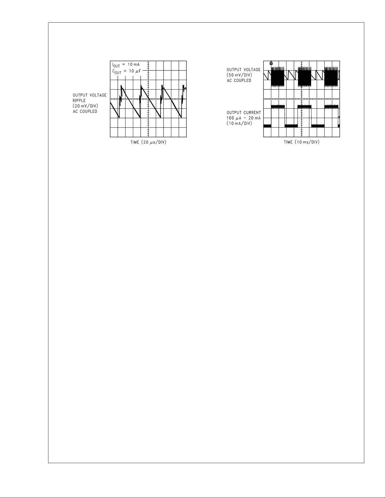
Application Information
OUTPUT VOLTAGE RIPPLE
The magnitude of the voltage ripple on the output of the
LM2760 is highly dependent on application conditions: output current and output capacitor properties, specifically. This
LM2760
www.national.com7
Page 8

Application Information (Continued)
is illustrated in Figure 1, which graphs of output voltage
LM2760
ripple versus input voltage for a few different output capacitor values.
FIGURE 1. Output Voltage Ripple vs. Input Voltage
=25oC)
(T
A
= 10mA, TA=25oC
I
OUT
Top: C
Mid: C
Bottom: C
In addition to the amount of output capacitance present, the
ESR of the output capacitor also affects output voltage
ripple. A low-ESR ceramic capacitor is recommended on the
output to keep output voltage ripple low. Placing multiple
capacitors is parallel can reduce ripple significantly, both by
increasing capacitance and reducing ESR. When capacitors
are in parallel, ESR is in parallel as well. The effective net
ESR is determined according to the properties of parallel
resistance. Two identical capacitors in parallel have twice the
capacitance and half the ESR as compared to a single
capacitor of the same make. On a similar note, if a largevalue, high-ESR capacitor (tantalum, for example) is to be
used as the primary output capacitor, the net output ESR can
be significantly reduced by placing a low-ESR ceramic capacitor in parallel with this primary output capacitor.
CAPACITORS
The LM2760 requires 3 external capacitors for proper operation. Surface-mount multi-layer ceramic capacitors are recommended. These capacitors are small, inexpensive and
have very low equivalent series resistance (≤10mΩ typ.).
Tantalum capacitors, OS-CON capacitors, and aluminum
electrolytic capacitors generally are not recommended for
use with the LM2760 due to their high ESR, as compared to
ceramic capacitors.
For most applications, ceramic capacitors with X7R or X5R
temperature characteristic are preferred for use with the
LM2760. These capacitors have tight capacitance tolerance
(as good as +/-10%), hold their value over temperature
(X7R: +/-15% over -55
o
Cto+85oC), and typically have little voltage coefficient.
-55
Capacitors with Y5V and/or Z5U temperature characteristic
are generally not recommended. These types of capacitors
typically have wide capacitance tolerance (+80%, -20%),
= 4.7µF
OUT
= 10µF
OUT
= 22µF
OUT
o
C to +125oC; X5R: +/-15% over
20044306
vary significantly over temperature (Y5V: +22%, -82% over
o
-35
Cto+85oC; Z5U: +22%, -56% over -10oCto+85oC), and
have poor voltage coefficients. Under some conditions, a
nominally 1µF Y5V or Z5U capacitor could have a capacitance of only 0.1µF. Such detrimental deviation is likely to
cause these Y5V and Z5U of capacitors to fail to meet the
minimum capacitance requirements of the LM2760.
The table below lists some leading ceramic capacitor manufacturers.
Manufacturer Contact Information
TDK www.component.tdk.com
AVX www.avx.com
Murata www.murata.com
Taiyo-Yuden www.t-yuden.com
Vishay-Vitramon www.vishay.com
INPUT CAPACITORS
The input capacitor (C
) is used as a reservoir of charge,
IN
helping to quickly transfer charge to the flying capacitor
during the charge phase (ø1) of operation. The input capacitor helps to keep the input voltage from drooping at the start
of the charge phase, when the flying capacitor is first connected to the input, and helps to filter noise on the input pin
that could adversely affect sensitive internal analog circuitry
biased off the input line. As mentioned above, an X7R/X5R
ceramic capacitor is recommended for use. An input capacitance of 4.7µF is recommended. It may be possible to reduce this value in applications where the maximum output
current is significantly less than 20mA. A smaller input capacitance typically results in higher input voltage ripple,
which may also show up as higher output voltage ripple as
well.
FLYING CAPACITORS
The flying capacitor (C
) transfers charge from the input to
FLY
the output, providing the voltage boost of the doubler. A
polarized capacitor (tantalum, aluminum electrolytic, etc.)
must not be used here, as the capacitor will be reversebiased upon start-up of the LM2760. For most applications, a
0.1µF X7R/X5R ceramic capacitor is recommended for C
FLY
Smaller flying capacitance typically will reduce the output
current capability of the part. The ESR also affects the output
current capability of the LM2760. For optimal performance, a
<
low-ESR ceramic capacitor (
10mΩ typ.) should be used.
Larger flying capacitance may increase output current capability, but it comes with the drawback of typically increasing
the magnitude of the output voltage ripple.
OUTPUT CAPACITOR
Both output capacitance and ESR of the LM2760 output
capacitor affect output voltage ripple. A low-ESR X7R/X5R
ceramic capacitor is the capacitor of choice for the LM2760
output. An output capacitance of 10µF is recommended for
most applications. Reducing output capacitance typically increases output voltage ripple. In applications where the
maximum output current is significantly less than 20mA,
output voltage ripple is less of a concern and it may be
desirable to reduce the output capacitance.
POWER EFFICIENCY
Efficiency of the LM2760 mirrors that of an unregulated
switched capacitor converter cascaded with a linear regulator when more-than nominal output current is present (≥
.
www.national.com 8
Page 9
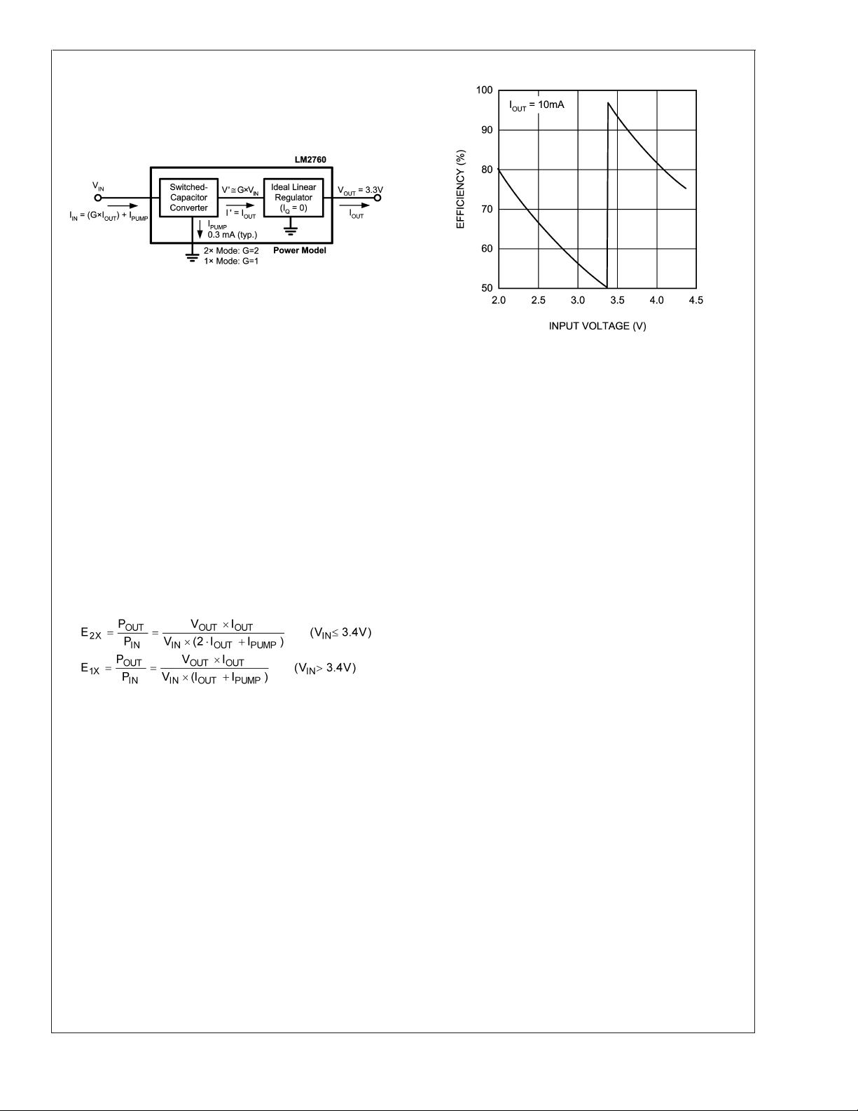
Application Information (Continued)
1mA). The simplified power model of the LM2760, in Figure
2, will be used to discuss power efficiency and power dissi-
pation.
20044304
FIGURE 2. LM2760 Power Model
LM2760
In calculating power efficiency, output power (P
OUT
) is easily
determined as the product of the output current and the 3.3V
output voltage. Like output current, input voltage is an
application-dependent variable. The input current can be
calculated using the principles of linear regulation and
switched capacitor conversion. In an ideal linear regulator,
the current into the circuit is equal to the current out of the
circuit. The principles of power conservation mandate the
ideal input current of a voltage converter must be equal to
the product of the gain of the converter and the output
current. When the input voltage is low (V
≤ 3.4V) and the
IN
LM2760 is in doubler mode (2x), the gain of the converter is
>
2. At higher input voltages (V
3.4V typ.) where the
IN
LM2760 is in pass mode (1x), the gain of the converter is 1.
Adding a correction factor for supply current when the pump
is continuously active (I
, 0.3mA typ.) gives an approxi-
PUMP
mation for total input current which, when combined with the
other input and output parameter(s), yields the following
equations for efficiency:
20044307
FIGURE 3.
A plot of efficiency versus input voltage, contained in Figure
4, gives a clear indication of how the pass mode improves
efficiency of the part at higher input voltages. Efficiency of
the part in both doubler and pass modes is inversely proportional to input voltage, highest when the input voltage is low.
When the part transitions to pass mode, however, there is a
boost in efficiency that is a result of the reduced input current
needed for the 1x-configured converter. This multi-gain topology maximizes LM2760 efficiency over the Li-Ion battery
input range: the average efficiency of the part over a 3.0Vto-4.2V input range is 75% (1mA ≤ I
OUT
≤ 20mA).
20044305
FIGURE 4. LM2760 Power Efficiency vs. Input Voltage
=25oC)
(T
A
Comparisons of LM2760 efficiency measurements to calculations using the above equations have shown the equations
to be quite accurate approximations of actual efficiency
when output currents are at or above 1mA. Under these
conditions, the pump is on nearly continuously, and PFMrelated rest states are infrequent. At lighter loads, however,
pulse frequency modulation has a greater impact on part
performance. With PFM, the part only pumps when it needs
to boost the output voltage. Otherwise, it idles in a lowcurrent rest mode. PFM reduces the input current of the part
(effectively reducing I
), improving the efficiency of the
PUMP
part at lighter loads.
POWER DISSIPATION
LM2760 power dissipation (P
) is calculated simply by sub-
D
tracting output power from input power. Maximum power
dissipation of the LM2760 occurs at the high end of the
doubler mode (V
= 3.4V). The following equation can be
IN
used to estimate power dissipation of the LM2760 when in
doubler mode:
P
D-2X=PIN-POUT
where I
PUMP
=[VINx (2·I
OUT+IPUMP
is the supply current when the pump is continu-
)]-[V
OUTxIOUT
ously active (0.3mA typ.).
Neglecting conditions outside the specified operating rat-
ings, maximum power dissipation of the LM2760 is approximately 70mW (V
) 3.4V, I
IN
When the junction-to-ambient thermal resistance of the
LM2760 in the application is 220
JESD51-3), power dissipation results in a 15
above ambient in the junction temperature of the part. Thus,
when the ambient temperature is 85
perature of the LM2760 under these conditions will be
o
C. LM2760 performance limits are guaranteed over a
100
junction temperature range of 0
= 20mA, I
OUT
o
o
Cto+70oC. The LM2760
PUMP
C/W (matches JEDEC
o
C, the junction tem-
o
C elevation
= 0.3mA).
must be operated with a junction temperature within this
range for the guaranteed performance limits listed in this
datasheet to apply.
],
www.national.com9
Page 10

Physical Dimensions inches (millimeters)
unless otherwise noted
5 Lead Small Outline Package (SOT-23-5)
MS05A
LM2760 3.3V Regulated Switched Capacitor Voltage Converter
LIFE SUPPORT POLICY
NATIONAL’S PRODUCTS ARE NOT AUTHORIZED FOR USE AS CRITICAL COMPONENTS IN LIFE SUPPORT
DEVICES OR SYSTEMS WITHOUT THE EXPRESS WRITTEN APPROVAL OF THE PRESIDENT AND GENERAL
COUNSEL OF NATIONAL SEMICONDUCTOR CORPORATION. As used herein:
1. Life support devices or systems are devices or
systems which, (a) are intended for surgical implant
into the body, or (b) support or sustain life, and
whose failure to perform when properly used in
accordance with instructions for use provided in the
labeling, can be reasonably expected to result in a
significant injury to the user.
National Semiconductor
Corporation
Americas
Email: support@nsc.com
www.national.com
National Semiconductor
Europe
Fax: +49 (0) 180-530 85 86
Email: europe.support@nsc.com
Deutsch Tel: +49 (0) 69 9508 6208
English Tel: +44 (0) 870 24 0 2171
Français Tel: +33 (0) 1 41 91 8790
2. A critical component is any component of a life
support device or system whose failure to perform
can be reasonably expected to cause the failure of
the life support device or system, or to affect its
safety or effectiveness.
National Semiconductor
Asia Pacific Customer
Response Group
Tel: 65-2544466
Fax: 65-2504466
Email: ap.support@nsc.com
National Semiconductor
Japan Ltd.
Tel: 81-3-5639-7560
Fax: 81-3-5639-7507
National does not assume any responsibility for use of any circuitry described, no circuit patent licenses are implied and National reserves the right at any time without notice to change said circuitry and specifications.
Page 11

 Loading...