


April 2005
LM2751
Regulated 2X, 1.5X Switched Capacitor White LED Driver
LM2751 Regulated 2X, 1.5X Switched Capacitor White LED Driver
General Description
The LM2751 is a constant frequency switched capacitor
charge pump with regulated output voltage options of 4.5V,
and 5.0V. Over the input voltage range of 2.8V to 5.5V the
LM2751 provides up to 150mA of output current and requires
only four low-cost ceramic capacitors.
The LM2751 provides excellent efficiency without the use of
an inductor by operating the charge pump in a gain of 3/2 or
2. The proper gain for maintaining regulation is chosen so
that efficiency is maximized over the input voltage range.
LM2751 uses constant frequency pre-regulation to minimize
conducted noise on the input and provide a predictable
switching frequency. The switching frequency is programmable to 725kHz, 300kHz, 37kHz, or 9.5kHz.
LM2751 is available in a 10-pin Leadless Leadframe NoPullback Package: LLP-10.
Typical Application Circuit
Features
n Regulated Output Options: 4.5V, 5.0V
n Output Voltage Regulated within 3%
n Peak Efficiency Over 90%
n 150mA (4.5V) or 80mA (5.0V) Output Current Capability
n Input Voltage Range: 2.8V to 5.5V
n Low Input and Output Voltage Ripple
<
n
1µA Typical Shutdown Current
n Small Solution Size - NO INDUCTOR
n Programmable 725kHz, 300kHz, 37kHz, or 9.5kHz
Switching Frequencies
n 10-pin LLP No-Pullback Package: 3mm x 3mm x 0.8mm
Applications
n White LED Display Backlights
n White LED Keypad Backlights
n General Purpose 2x, 1.5x Regulated Charge Pump
20112101
LM2751 2x/1.5x Efficiency vs.
2x Charge Pump Effciency
20112128
© 2005 National Semiconductor Corporation DS201121 www.national.com

Connection Diagram
LM2751
Pin Descriptions
#
Pin
1V
2C
3V
4 CS0 Frequency Select Input 0.
5 CS1 Frequency Select Input 1.
6 EN Enable Pin Logic Input.
7C
8 GND Ground.
9C
10 C
10-pin Leadless Leadframe Package (LLP-10) No Pullback
3mm x 3mm x 0.8mm
NS Package Number SDA10A
Name Description
OUT
1+
IN
2−
1−
2+
Pre-Regulated Output.
Flying Capacitor C1 Connection.
Input Supply Range: 2.8V to 5.5V.
Flying Capacitor C2 Connection.
Flying Capacitor C1 Connection.
Flying Capacitor C2 Connection.
20112102
Ordering Information
Version Voltage Option Order Number Package Marking Supplied As Tape and
A 5.0V LM2751SD-A XXXXX
A 5.0V LM2751SDX-A 4500 Units
B 4.5V LM2751SD-B XXXXX
B 4.5V LM2751SDX-B 4500 Units
www.national.com 2
Reel
1000 Units
YYYYY = L145B
1000 Units
YYYYY = L146B

LM2751
Absolute Maximum Ratings (Notes 1, 2)
If Military/Aerospace specified devices are required,
please contact the National Semiconductor Sales Office/
Distributors for availability and specifications.
Pin −0.3V to 6.0V
V
IN
EN, CS0, CS1 Pins −0.3V to (V
Continuous Power Dissipation
(Note 3) Internally Limited
Junction Temperature
(T
J-MAX-ABS
) 150˚C
Storage Temperature Range −65˚C to 150˚C
Maximum Lead Temperature 265˚C
(Soldering, 10sec.)
ESD Rating (Note 4)
Human-body model:
Machine model:
+0.3)
IN
w/ 6.0V max
2kV
200V
Operating Ratings (Notes 1, 2)
Input Voltage Range 2.8V to 5.5V
EN, CS0, CS1 Input Voltage Range 0V to V
Junction Temperature (TJ) Range -40˚C to 115˚C
Ambient Temperature (T
(Note 5)
Recommended Maximum Load Current
Version Freq. = 725kHz 150mA
B Freq. = 300kHz 120mA
Version Freq. = 725kHz 80mA
A Freq. = 300kHz 60mA
) Range -40˚C to 85˚C
A
Freq. = 37kHz 40mA
Freq. = 9.5kHz 10mA
Freq. = 37kHz 16mA
Freq. = 9.5kHz 4mA
Thermal Properties
Junction-to-Ambient Thermal
Resistance, LLP-10 55˚C/W
Package (θ
) (Note 6)
JA
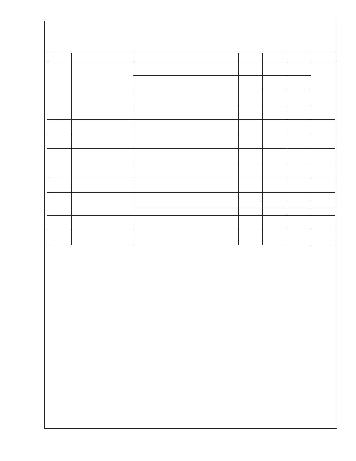
Electrical Characteristics (Notes 2, 7)
Limits in standard typeface are for TA=25oC. Limits in boldface type apply over the full operating ambient temperature range
(-40˚C ≤ T
= 3.6V, V(EN) = V
Symbol Parameter Conditions Min Typ Max Units
V
OUT
V
R
I
Q
I
SD
E Efficiency I
≤ +85˚C) . Unless otherwise noted, specifications apply to the LM2751 Typical Application Circuit (pg. 1) with: V
A
Output Voltage Version A, 2.8V ≤ VIN≤ 5.5V,
Output Ripple 2.8V ≤ VIN≤ 5.5V
Quiescent Current Freq. = 9.5kHz, I
CS0=CS1=VIN,C1=C2= 1.0µF, CIN=C
IN,
Freq. = 300kHz, 725kHz, T
= 0 to 60mA
I
OUT
Version A, 2.8V ≤ V
Freq. = 300kHz, I
Freq. = 725kHz, I
Version B, 2.8V ≤ V
IN
OUT
OUT
IN
Freq. = 300kHz, 725kHz, T
= 0 to 120mA
I
OUT
Version B, 2.8V ≤ V
Freq. = 300kHz, I
Freq. = 725kHz, I
= 60mA
I
OUT
Freq. = 37kHz, I
Freq. = 300kHz, I
Freq. = 725kHz, I
IN
OUT
OUT
OUT
= 0mA, VIN= 3.7V 450 640
OUT
OUT
OUT
= 2.2µF (Note 8).
OUT
= 25˚C
A
≤ 5.5V,
= 0 to 60mA
4.850
(-3%)
4.775
(-4.5%)
5.0 5.150
(+3%)
5.225
(+4.5%)
= 0 to 80mA
≤ 5.5V,
= 25˚C
A
≤ 5.5V,
= 0 to 120mA
4.343
(-3.5%)
4.275
(-5%)
4.5 4.658
(+3.5%)
4.725
(+5%)
= 0 to 150mA
8mV
= 0mA, VIN= 3.7V 425 600 µA
= 0mA, VIN= 3.7V 700 900
= 0mA, VIN= 3.7V 1000 1500
Shutdown Supply Current V(EN) = 0V 0.77 1.3 µA
V(EN) = 0V, T
= 80mA (Version A, 5.0V)
OUT
= 85˚C 1.0
A
92 %
Freq. = 300kHz, 725kHz
= 150mA (Version B, 4.5V)
I
OUT
83
Freq. = 300kHz, 725kHz
IN
IN
V
www.national.com3
Electrical Characteristics (Notes 2, 7) (Continued)
Limits in standard typeface are for TA=25oC. Limits in boldface type apply over the full operating ambient temperature range
LM2751
(-40˚C ≤ T
= 3.6V, V(EN) = V
Symbol Parameter Conditions Min Typ Max Units
fsw Switching Frequency CS0 = High, CS1 = Low
V
IH
V
IL
I
IH
I
IL
V
G
I
SC
t
ON
Note 1: Absolute Maximum Ratings indicate limits beyond which damage to the component may occur. Operating Ratings are conditions under which operation of
the device is guaranteed. Operating Ratings do not imply guaranteed performance limits. For guaranteed performance limits and associated test conditions, see the
Electrical Characteristics tables.
Note 2: All voltages are with respect to the potential at the GND pin.
Note 3: Internal thermal shutdown circuitry protects the device from permanent damage. Thermal shutdown engages at T
T
=140˚C (typ.).
J
Note 4: The Human body model is a 100 pF capacitor discharged through a 1.5kΩ resistor into each pin. The machine model is a 200pF capacitor discharged
directly into each pin. MIL-STD-883 3015.7
Note 5: In applications where high power dissipation and/or poor package thermal resistance is present, the maximum ambient temperature may have to be
derated. Maximum ambient temperature (T
dissipation of the device in the application (P
following equation: T
Note 6: Junction-to-ambient thermal resistance (θ
standard JESD51-7. The test board is a 4 layer FR-4 board measuring 102mm x 76mm x 1.6mm witha2x1array of thermal vias. The ground plane on the board
is 50mm x 50mm. Thickness of copper layers are 36µm/18µm /18µm/36µm (1.5oz/1oz/1oz/1.5oz). Ambient temperature in simulation is 22
dissipation is 1W.
The value of θ
conditions. In applications where high maximum power dissipation exists (high V
information on these topics, please refer to Application Note 1187: Leadless Leadframe Package (LLP) and the Power Efficiency and Power Dissipation
section of this datasheet.
Note 7: Min and Max limits are guaranteed by design, test, or statistical analysis. Typical numbers are not guaranteed, but represent the most likely norm.
Note 8: C
Note 9: EN Logic Input High Current (I
Note 10: Turn-on time is measured from when the EN signal is pulled high until the output voltage on V
≤ +85˚C) . Unless otherwise noted, specifications apply to the LM2751 Typical Application Circuit (pg. 1) with: V
A
Logic Input High Input Pins: EN, CS0, CS1
Logic Input Low Input Pins: EN, CS0, CS1
Logic Input High Current Input Pins: CS0, CS1
CS0=CS1=VIN,C1=C2= 1.0µF, CIN=C
IN,
2.8V ≤ V
IN
≤ 5.5V
CS0 = Low, CS1 = Low
2.8V ≤ VIN≤ 5.5V
CS0 = Low, CS1 = High
2.8V ≤ VIN≤ 5.5V
CS0 = High, CS1 = High
2.8V ≤ V
2.8V ≤ V
2.8V ≤ V
IN
IN
IN
≤ 5.5V
≤ 5.5V
≤ 5.5V
= 2.2µF (Note 8).
OUT
6.7
(−30%)
26
(−30%)
210
(−30%)
508
(−30%)
1.00 V
9.5 12.3
(+30%)
37 48
(+30%)
300 390
(+30%)
725 942
(+30%)
IN
0 .30 V
10 nA
V(CSx) = 1.8V
Input Pin: EN
2µA
V(EN) = 1.8V(Note 9)
Logic Input Low Current Input Pins: EN, CS0, CS1
10 nA
V(EN, CSx) = 0V
Gain Transition Voltage
(Version A, B)
1.5X to 2X 3.50 V
2X to 1.5X 3.58
Hysteresis 40 80 150 mV
Short Circuit Output
V
= 0V 250 mA
OUT
Current
V
Turn-On Time
OUT
300 µs
(Note 10)
=150˚C (typ.) and disengages at
J
) is dependent on the maximum operation junction temperature (T
A-MAX
), and the junction-to ambient thermal resistance of the part/package in the application (θJA), as given by the
D-MAX
A-MAX=TJ-MAX-OP
of the LM2751 in LLP-10 could fall in a range as wide as 50oC/W to 150oC/W (if not wider), depending on PWB material, layout, and environmental
JA
IN,COUT,C1
, and C2: Low-ESR Surface-Mount Ceramic Capacitors (MLCCs) used in setting electrical characteristics.
-(θJAxP
)isduetoa1MΩ(typ.) pull-down resistor connected internally between the EN pin and GND.
IH
).
D-MAX
) is taken from a thermal modeling result, performed under the conditions and guidelines set forth in the JEDEC
JA
, high I
IN
), special care must be paid to thermal dissipation issues. For more
OUT
crosses 90% of its final value.
OUT
=115oC), the maximum power
J-MAX-OP
o
C, still air. Power
IN
kHz
V
www.national.com 4

Block Diagram
LM2751
20112103
www.national.com5

Typical Performance Characteristics Unless otherwise specified: T
CS1=V
LM2751
, V(EN) = VIN,CIN=C
IN
Output Voltage vs. Output Current,
Version A (5V), 300kHz
= 2.2µF, C1=C2= 1µF.
OUT
Output Voltage vs. Output Current,
= 25˚C, VIN= 3.6V, CS0 =
A
Version B (4.5V), 300kHz
Output Voltage vs. Output Current,
Version A (5V), 725kHz
Input Current vs. Input Voltage,
Version A (5V)
20112110
20112116
Output Voltage vs. Output Current,
Version B (4.5V), 725kHz
20112111 20112117
Input Current vs. Input Voltage,
Version B (4.5V)
20112115 20112121
www.national.com 6

LM2751
Typical Performance Characteristics Unless otherwise specified: T
, V(EN) = VIN,CIN=C
=V
IN
Output Voltage vs. Input Voltage,
Output Voltage vs. Input Voltage,
Version A (5V), 300kHz
Version A (5V), 725kHz
= 2.2µF, C1=C2= 1µF. (Continued)
OUT
20112112 20112118
Output Voltage vs. Input Voltage,
Version B (4.5V), 300kHz
Output Voltage vs. Input Voltage,
Version B (4.5V), 725kHz
= 25˚C, VIN= 3.6V, CS0 = CS1
A
Efficiency vs. Input Voltage,
Version A (5V)
20112113 20112119
Efficiency vs. Input Voltage,
Version B (4.5V)
20112114 20112120
www.national.com7

Typical Performance Characteristics Unless otherwise specified: T
=V
LM2751
, V(EN) = VIN,CIN=C
IN
Output Voltage Ripple vs. Input Voltage
Version B (4.5V), Load = 120mA
= 2.2µF, C1=C2= 1µF. (Continued)
OUT
= 25˚C, VIN= 3.6V, CS0 = CS1
A
Output Voltage Ripple,
Version B (4.5V)
Line Step Response,
Version B (4.5V)
VIN= 3.2V - 4.2V Step, Load = 150mA
CH1 (top): V
CH2: V
Time scale: 200µs/Div
; Scale: 1V/Div, DC Coupled
IN
; Scale: 50mV/Div, AC Coupled
OUT
Start-up Behavior,
Version A (5V), Load = 80mA
20112124
20112129
VIN= 3.6V, Load = 150mA
CH1: V
Time scale: 400ns/Div
; Scale: 10mV/Div, AC Coupled
OUT
Load Step Response,
Version B (4.5V)
VIN= 3.6V, Load = 20mA - 150mA Step
CH1 (top): V
CH2: Output Current; Scale: 50mA/Div
Time scale: 200µs/Div
; Scale: 50mV/Div, AC Coupled
OUT
Start-up Behavior,
Version B (4.5V), Load = 150mA
20112126
20112127
CH1: EN pin; Scale: 2V/Div
CH2: V
Time scale: 100µs/Div
; Scale: 2V/Div
OUT
20112122
www.national.com 8
CH1: EN pin; Scale: 2V/Div
CH2: V
Time scale: 100µs/Div
; Scale: 2V/Div
OUT
20112123

Application Information
CIRCUIT DESCRIPTION
The LM2751 is a Switched Capacitor Convertor with gains of
2x and 1.5x. It is capable of continuously supplying up to
150mA at 4.5V or up to 80mA at 5V depending on the output
voltage option. The LM2751’s fixed frequency pre-regulation
maintains the output voltage to within 3% (typ.), making it
well suited for driving White LEDs. There are also four user
programmable switching frequencies to reduce the quiescent current consumption at light loads.
Aside from powering LEDs, the LM2751 is suitable for driving other devices with power requirements up to 150mA. The
LM2751 operates over the extended Li-Ion battery range
from 2.8V to 5.5V. The LM2751 limits output current to
250mA (typ.) during an output short circuit condition. LED
brightness is controlled by applying a PWM (Pulse Width
Modulation) signal to the Enable pin (EN). (see PWM
BRIGHTNESS CONTROL section).
SOFT START
Soft Start is engaged when the device is taken out of Shutdown mode (EN = logic HIGH) or when voltage is supplied
simultaneously to the V
voltage on V
will ramp up in proportion to the rate that the
OUT
reference voltage is being ramped up. The output voltage is
programmed to rise from 0V to the regulated output voltage
level (4.5V or 5V) in 300µs (typ.).
ENABLE MODE
The Enable logic pin (EN) disables the part and reduces the
quiescent current to 0.77µA (typ.). The LM2751 has an
active-high enable pin (LOW = shut down, HIGH = operating) which can be driven with a low-voltage CMOS logic
signal (1.5V logic, 1.8V logic, etc). There is an internal 1MΩ
pull-down resistor between the EN and GND pins of the
LM2751.
FREQUENCY MODE SELECT
The LM2751 switching frequency is user programmable via
two logic input pins, CS0 and CS1. Both logic input pins have
active-high logic (LOW = un-selected, HIGH = selected) and
can be driven with a low-voltage CMOS logic signal (1.5V
logic, 1.8V logic, etc). There are no internal pull-down or
pull-up resistors between the CSx and GND pins of the
LM2751. The CSO and CS1 can be controlled independently
or with the same logic signal.
The selectable switching frequencies are 9.5kHz, 37kHz,
300kHz, 725kHz. The switching frequency is programmed
according to Table 1
TABLE 1. Frequency Modes
CS0 CS1 Frequency
0 0 37kHz
0 1 300kHz
1 0 9.5kHz
1 1 725kHz
V
REGULATION
OUT
The LM2751 uses pre-regulation to regulate the output voltage to 4.5V or 5.0V depending on the voltage option. Preregulation uses the voltage present at V
and EN pins. During Soft Start, the
IN
to limit the gate
OUT
drive of the switched capacitor charge pump. This regulation
is done before the voltage is gained up by the charge pump,
giving rise to the term "pre-regulation". Pre-regulation helps
to reduce input current noise and large input current spikes
normally associated with switched capacitor charge pumps.
The LM2751 switched capacitor charge pump has gains of
2x and 1.5x. When the input voltage to the device is greater
than 3.58V (typ.), the LM2751 operates in a gain of 1.5x.
When the input voltage falls below 3.5V (typ.), the device
switches to a gain of 2x.
OUTPUT VOLTAGE RIPPLE
The primary contributor in keeping the output voltage ripple
of the LM2751 low is its switching topology. The output
capacitance, input voltage, switching frequency and output
current also play a significant part in determining the output
voltage ripple. Due to the complexity of the LM2751 operation, providing equations or models to approximate the magnitude of the ripple cannot be easily accomplished. However,
the following general statements can be made.
The LM2751 has very low output ripple when compared to
typical boost regulators due to its double-pump topology,
where charge is continually supplied to the output during
both 2x and 1.5x modes. Combined with fixed frequency
operation modes, double-pumping allows for the use of a
very small, low value ceramic capacitor on the output node
while still achieving minimal output ripple. Increasing the
capacitance by adding a higher value capacitor or placing
multiple capacitors in parallel can further reduce the ripple
magnitude.
CAPACITOR SELECTION
The LM2751 requires 4 external capacitors for proper operation. Surface-mount multi-layer ceramic capacitors are recommended. These capacitors are small, inexpensive and
have very low equivalent series resistance (ESR, ≤15mΩ
typ.). Tantalum capacitors, OS-CON capacitors, and aluminum electrolytic capacitors are generally not recommended
for use with the LM2751 due to their high ESR, as compared
to ceramic capacitors.
For most applications, ceramic capacitors with X7R or X5R
temperature characteristic are preferred for use with the
LM2751. These capacitors have tight capacitance tolerance
±
(as good as
±
15% over −55˚C to 125˚C; X5R:±15% over −55˚C to
10%), hold their value over temperature (X7R:
85˚C), and typically have little voltage coefficient when compared to other types of capacitors. However selecting a
capacitor with a voltage rating much higher than the voltage
it will be subjected to, will ensure that the capacitance will
stay closer to the capacitor’s nominal value. Capacitors with
Y5V or Z5U temperature characteristic are generally not
recommended for use with the LM2751. Capacitors with
these temperature characteristics typically have wide capacitance tolerance (+80%, −20%), vary significantly over
temperature (Y5V: +22%, −82% over −30˚C to +85˚C range;
Z5U: +22%, −56% over +10˚C to +85˚C range), and have
poor voltage coefficients. Under some conditions, a nominal
1µF Y5V or Z5U capacitor could have a capacitance of only
0.1µF. Such detrimental deviation is likely to cause Y5V and
Z5U capacitors to fail to meet the minimum capacitance
requirements of the LM2751.
LM2751
www.national.com9

Application Information (Continued)
The voltage rating of the output capacitor should be 10V or
LM2751
more. All other capacitors should have a voltage rating at or
above the maximum input voltage of the application.
DRIVING WHITE LEDS
The desired LED current is set by placing a resistor (R) in
series with each LED, and is determined by the equation:
=(V
I
LED
In the equation above, I
a particular LED, and V
OUT-VLED
is the current that flows through
LED
is the forward voltage of the LED
LED
at the given current. The output voltage (V
LM2751 is tightly regulated to 4.5V or 5V depending on the
output voltage option. However, LED forward voltage varies
from LED to LED, and LED current will vary accordingly.
Mismatch of LED currents will result in brightness mismatch
from one LED to the next. Therefore it is suggested that LED
groups with tightly controlled I-V characteristics ("Binned"
LEDs) be used. LEDs with looser tolerance can be used in
applications where brightness matching is not critical, such
as in keypad or general backlighting. The typical and maximum diode forward voltage depends highly on the manufacturer and their technology.
PWM BRIGHTNESS CONTROL
Perceived LED brightness can be adjusted using a PWM
control signal on the Enable pin of the LM2751, to turn the
voltage output ON and OFF at a rate faster than perceptible
by the eye. When this is done, the total brightness perceived
is proportional to the duty cycle (D) of the PWM signal (D =
the percentage of time that the LED is on in every PWM
cycle). A simple example: if the LEDs are driven at 15mA
each with a PWM signal that has a 50% duty cycle, perceived LED brightness will be about half as bright as compared to when the LEDs are driven continuously with 15mA.
For linear brightness control over the full duty cycle adjustment range, the PWM frequency (f) should be limited to
accommodate the turn-on time (typ. T
device.
D x (1/f)
f
MAX=DMIN÷TON
The minimum recommended PWM frequency is 100Hz. Frequencies below this may be visibly noticeable as flicker or
blinking. The maximum recommended PWM frequency is
1kHz. Frequencies above this may cause noise in the audible range.
)÷R
= 300µs) of the
ON
>
T
ON
)ofthe
OUT
THERMAL PROTECTION
When the junction temperature exceeds 150˚C (typ.), internal thermal protection circuitry disables the device. This
feature protects the LM2751 from damage due to excessive
power dissipation. The device will recover and operate normally when the junction temperature falls below 140˚C (typ.).
It is important to have good thermal conduction with a proper
layout to reduce thermal resistance.
POWER EFFICIENCY
Charge-Pump efficiency is derived in the following two ideal
equations (supply current and other losses are neglected for
simplicity):
=GxI
I
E=(V
OUTxIOUT
IN
)÷(VINxIIN)=V
OUT
OUT
÷(GxVIN)
In the equations, G represents the charge pump gain. Efficiency is at its highest asGxV
approaches V
IN
OUT
. Refer to
the efficiency graph in the Typical Performance Character-
istics section for the detailed efficiency data.
POWER DISSIPATION
The power dissipation (P
) can be approximated with the equations below. P
ture (T
J
DISSIPATION
is the product of the input current and input voltage, P
) and junction tempera-
OUT
the power consumed by the load connected to the output,
is the ambient temperature, and θJAis the junction-to-
T
A
ambient thermal resistance for the LLP-10 package. V
the input voltage to the LM2751, V
output of the device, and I
the load connected to V
P
DISSIPATION=PIN-POUT
is the total current supplied to
OUT
.
OUT
=(VINxIIN)−(V
J=TA
+(P
DISSIPATION
T
is the voltage at the
VOUT
VOUTxIOUT
x θJA)
)
IN
The junction temperature rating takes precedence over the
ambient temperature rating. The LM2751 may be operated
outside the ambient temperature rating, so long as the junction temperature of the device does not exceed the maximum operating rating of 115˚C. The maximum ambient temperature rating must be derated in applications where high
power dissipation and/or poor thermal resistance causes the
junction temperature to exceed 115˚C.
IN
is
is
www.national.com 10

Physical Dimensions inches (millimeters) unless otherwise noted
LM2751 Regulated 2X, 1.5X Switched Capacitor White LED Driver
10-Pin LLP
NS Package Number SDA10A
National does not assume any responsibility for use of any circuitry described, no circuit patent licenses are implied and National reserves
the right at any time without notice to change said circuitry and specifications.
For the most current product information visit us at www.national.com.
LIFE SUPPORT POLICY
NATIONAL’S PRODUCTS ARE NOT AUTHORIZED FOR USE AS CRITICAL COMPONENTS IN LIFE SUPPORT DEVICES OR SYSTEMS
WITHOUT THE EXPRESS WRITTEN APPROVAL OF THE PRESIDENT AND GENERAL COUNSEL OF NATIONAL SEMICONDUCTOR
CORPORATION. As used herein:
1. Life support devices or systems are devices or systems
which, (a) are intended for surgical implant into the body, or
(b) support or sustain life, and whose failure to perform when
properly used in accordance with instructions for use
2. A critical component is any component of a life support
device or system whose failure to perform can be reasonably
expected to cause the failure of the life support device or
system, or to affect its safety or effectiveness.
provided in the labeling, can be reasonably expected to result
in a significant injury to the user.
BANNED SUBSTANCE COMPLIANCE
National Semiconductor manufactures products and uses packing materials that meet the provisions of the Customer Products
Stewardship Specification (CSP-9-111C2) and the Banned Substances and Materials of Interest Specification (CSP-9-111S2) and contain
no ‘‘Banned Substances’’ as defined in CSP-9-111S2.
National Semiconductor
Americas Customer
Support Center
Email: new.feedback@nsc.com
Tel: 1-800-272-9959
www.national.com
National Semiconductor
Europe Customer Support Center
Fax: +49 (0) 180-530 85 86
Email: europe.support@nsc.com
Deutsch Tel: +49 (0) 69 9508 6208
English Tel: +44 (0) 870 24 0 2171
Français Tel: +33 (0) 1 41 91 8790
National Semiconductor
Asia Pacific Customer
Support Center
Email: ap.support@nsc.com
National Semiconductor
Japan Customer Support Center
Fax: 81-3-5639-7507
Email: jpn.feedback@nsc.com
Tel: 81-3-5639-7560
 Loading...