

Page 1
LM2750
Low Noise Switched Capacitor Boost Regulator
LM2750 Low Noise Switched Capacitor Boost Regulator
December 2005
General Description
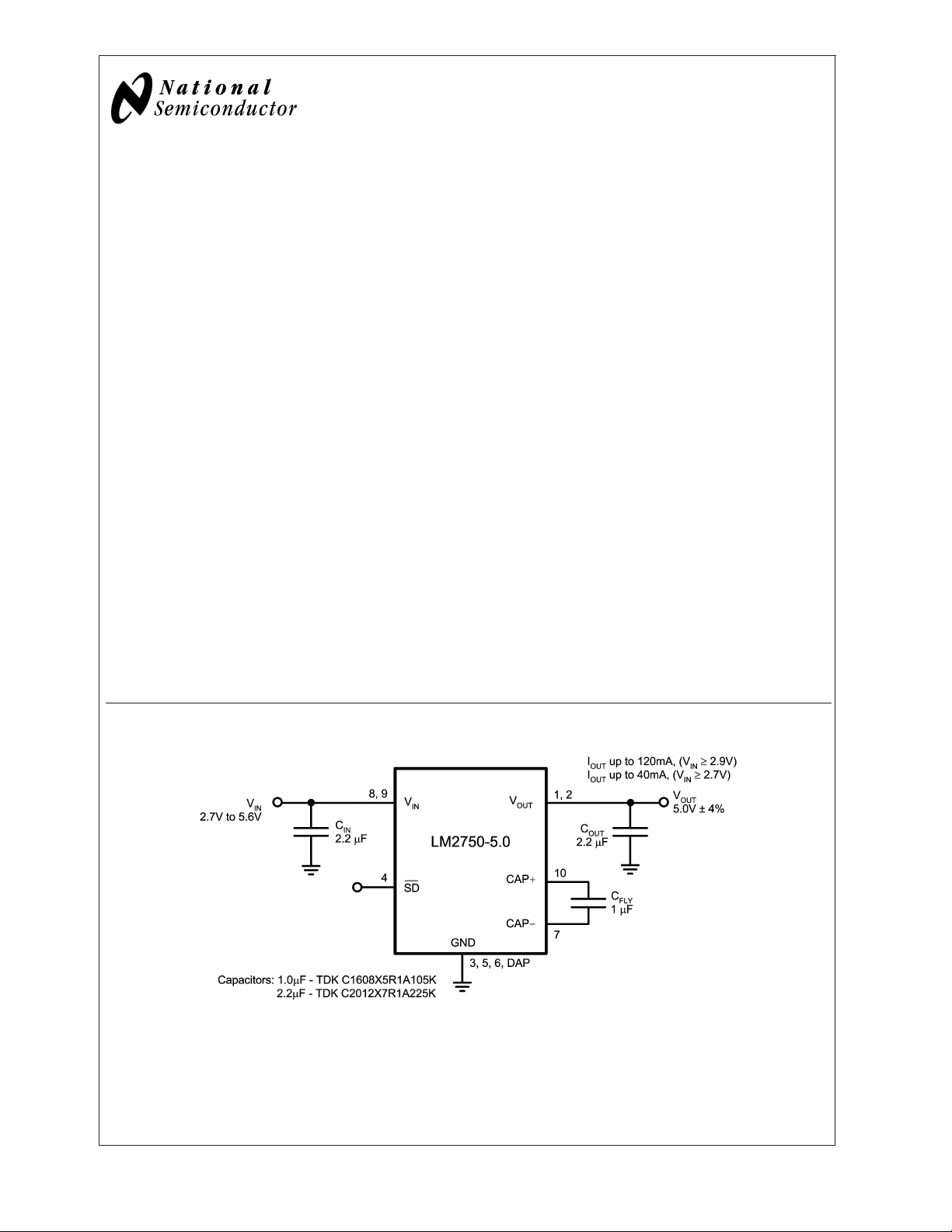
The LM2750 is a regulated switched-capacitor doubler that
produces a low-noise output voltage. The 5.0V output voltage option (LM2750-5.0) can supply up to 120mA of output
current over a 2.9V to 5.6V input range, as well as up to
40mA of output current when the input voltage is as low as
2.7V. An adjustable output voltage option with similar output
current capabilities is also available (LM2750-ADJ). The
LM2750 has been placed in National’s 10-pin LLP, a package with excellent thermal properties that keeps the part
from overheating under almost all rated operating conditions
A perfect fit for space-constrained, battery-powered applications, the LM2750 requires only 3 external components: one
input capacitor, one output capacitor, and one flying capacitor. Small, inexpensive ceramic capacitors are recommended for use. These capacitors, in conjunction with the
1.7MHz fixed switching frequency of the LM2750, yield low
output voltage ripple, beneficial for systems requiring a lownoise supply. Pre-regulation minimizes input current ripple,
reducing input noise to negligible levels.
A tightly controlled soft-start feature limits inrush currents
during part activation. Shutdown completely disconnects the
load from the input. Output current limiting and thermal
shutdown circuitry protect both the LM2750 and connected
devices in the event of output shorts or excessive current
loads.
Features
n Inductorless solution: Application requires only 3 small
ceramic capacitors
n Fixed 5.0V output and adjustable output voltage options
available
n 85% Peak Efficiency
70% Average Efficiency over Li-Ion Input Range
(2.9V-to-4.2V)
n Output Current up to 120mA with 2.9V ≤ V
Output Current up to 40mA with 2.7V ≤ V
n Wide Input Voltage Range: 2.7V to 5.6V
n Fixed 1.7MHz switching frequency for a low-noise,
low-ripple output signal
n Pre-regulation minimizes input current ripple, keeping
the battery line (V
n Tiny LLP package with outstanding power dissipation:
Usually no derating required.
n Shutdown Supply Current less than 2µA
) virtually noise-free
IN
IN
IN
≤ 5.6V
≤ 2.9V
Applications
n White and Colored LED-based Display Lighting
n Cellular Phone SIM cards
n Audio Amplifier Power Supplies
n General Purpose Li-Ion-to-5V Conversion
Typical Application Circuit
20035101
© 2005 National Semiconductor Corporation DS200351 www.national.com
Page 2
Connection Diagram
LM2750
LM2750
10-Pin Leadless Leadframe Package (LLP) - 3mm X 3mm
NS Package Number LDA10A (Shown below), and SDA10A
Pin Names and Numbers apply to both SDA10A and LDA10A packages.
20035102
Pin Descriptions
Pin #(s) Pin Name Description
8, 9 V
1, 2 V
10 CAP+ Flying Capacitor Positive Terminal
7 CAP- Flying Capacitor Negative Terminal
4SD
3
5, 6, DAP GND Ground - These pins must be connected externally.
LM2750-5.0: GND
LM2750-ADJ: FB Feedback Pin
IN
OUT
Input Voltage - The pins must be connected externally.
Output Voltage - These pins must be connected externally.
Active-Low Shutdown Input. A 200kΩ resistor is connected internally between
this pin and GND to pull the voltage on this pin to 0V, and shut down the part,
when the pin is left floating.
This pin must be connected exernally to the ground pins (pins 5, 6, and the
DAP).
Ordering Information
Output Voltage
Option
5.0 LM2750LD-5.0 LDA10A S002B 1000 Units, Tape and Reel
5.0 LM2750LDX-5.0 LDA10A S002B 4500 Units, Tape and Reel
Adjustable LM2750LD-ADJ LDA10A S003B 1000 Units, Tape and Reel
Adjustable LM2750LDX-ADJ LDA10A S003B 4500 Units, Tape and Reel
5.0 LM2750SD-5.0 SDA10A S005B 1000 Units, Tape and Reel
5.0 LM2750SDX-5.0 SDA10A S005B 4500 Units, Tape and Reel
Adjustable LM2750SD-ADJ SDA10A S004B 1000 Units, Tape and Reel
Adjustable LM2750SDX-ADJ SDA10A S004B 4500 Units, Tape and Reel
Note 1: LDA10A Package: 10 pad pullback LLP. SDA10A Package: 10 pad non-pullback LLP. For more details, refer to the package drawings in the Physical
Dimensions section at the end of this datasheet.
Ordering
Information
Package
(Note 1)
Package
Marking
Supplied as
www.national.com 2
Page 3
LM2750
Absolute Maximum Ratings (Notes 2, 3)
If Military/Aerospace specified devices are required,
please contact the National Semiconductor Sales Office/
Distributors for availability and specifications.
Pin: Voltage to Ground −0.3V to 6V
V
IN
SD Pin: Voltage to GND
Junction Temperature (T
J-MAX-ABS
) 150˚C
Continuous Power Dissipation Internally Limited
(Note 4)
Maximum Output Current (Note 5) 175mA
Storage Temperature Range −65˚C to 150˚C
Maximum Lead Temperature 260˚C
−0.3V to
+0.3V)
(V
IN
Operating Ratings (Notes 2, 3)
LM2750-5.0 Input Voltage Range 2.7V to 5.6V
LM2750-ADJ Input Voltage Range
3.8V ≤ V
4.9V ≤ V
LM2750-ADJ Output Voltage Range 3.8V to 5.2V
Recommended Output Current
2.9V ≤ V
2.7V ≤ V
Junction Temperature (T
Ambient Temperature (T
(Note 7)
≤ 4.9V: 2.7V to (V
OUT
≤ 5.2V: 2.7V to 5.6V
OUT
≤ 5.6V 0 to 120mA
IN
≤ 2.9V 0 to 40mA
IN
) Range -40˚C to 125˚C
J
) Range -40˚C to 85˚C
A
OUT
(Soldering, 5 sec.)
ESD Rating (Note 6)
Human-body model:
Machine model
2kV
100V
Thermal Information
Junction-to-Ambient Thermal
Resistance, LLP-10 55˚C/W
Package (θJA) (Note 8)
Electrical Characteristics (Notes 3, 9)
Typical values and limits in standard typeface apply for TJ=25oC. Limits in boldface type apply over the operating junction
temperature range. Unless otherwise specified: 2.9V ≤ V
= 2 x 1µF, C
= 2 x 1µF (Note 10).
OUT
≤ 5.6V, V
IN
Symbol Parameter Conditions Min Typ Max Units
2.9V ≤ V
V
OUT
I
Q
I
SD
V
FB
Output Voltage
(LM2750-5.0)
Operating Supply Current I
Shutdown Supply Current V(SD) = 0V 2 µA
Feedback Pin Voltage
I
OUT
2.7V ≤ V
I
OUT
OUT
V
IH(MIN)
VIN= 3.1V 1.170 1.232 1.294 V
≤ 5.6V,
IN
≤ 120mA
≤ 2.9V,
IN
≤ 40mA
= 0mA,
≤ V(SD) ≤V
(LM2750-ADJ)
I
FB
Feedback Pin Input Current
VFB= 1.4V 1 nA
(LM2750-ADJ)
V
E
E
f
t
R
PEAK
AVG
SW
ON
Output Ripple C
Peak Efficiency
(LM2750-5.0)
Average Efficiency over Li-Ion
Input Range
(LM2750-5.0)
(Note 12)
= 10µF, I
OUT
C
= 2.2µF, I
OUT
VIN= 2.7V, I
V
= 2.9V, I
IN
Range: 2.9V - 4.2V,
V
IN
I
OUT
V
Range: 2.9V - 4.2V,
IN
I
OUT
OUT
OUT
= 120mA
= 40mA
Switching Frequency 1.0 1.7 MHz
V
Turn-On Time VIN= 3.0V, I
OUT
OUT
(Note 11)
I
LIM
Current Limit V
shorted to GND 300 mA
OUT
Shutdown Pin (SD) Characteristics
V
IH
V
IL
I
IH
I
IL
Logic-High SD Input 1.3 V
Logic-Low SD Input 0 0.4 V
SD Input Current (Note 13) 1.3V ≤ V(SD) ≤ V
SD Input Current V(SD) = 0V −1 1 µA
= 5.0V (LM2750-ADJ), V(SD) = VIN,C
OUT
4.80
5.0 5.20
(-4%)
4.80
5.0 5.20
(-4%)
FLY
(+4%)
(+4%)
= 1µF, C
51012mA
IN
= 100mA 4
OUT
= 100mA 15
OUT
= 40mA 87 %
= 120mA 85
70 %
67
= 100mA,
IN
0.5 ms
IN
15 50 µA
+0.7V)
IN
V
(%)
mVp-p
V
www.national.com3
Page 4
Electrical Characteristics (Notes 3, 9) (Continued)
Typical values and limits in standard typeface apply for TJ=25oC. Limits in boldface type apply over the operating junction
LM2750
temperature range. Unless otherwise specified: 2.9V ≤ V
= 2 x 1µF, C
= 2 x 1µF (Note 10).
OUT
Symbol Parameter Conditions Min Typ Max Units
Capacitor Requirements
C
IN
C
OUT
Required Input
Capacitance(Note 14)
Required Output
Capacitance(Note 14)
Note 2: Absolute Maximum Ratings indicate limits beyond which damage to the component may occur. Operating Ratings are conditions under which operation of
the device is guaranteed. Operating Ratings do not imply guaranteed performance limits. For guaranteed performance limits and associated test conditions, see the
Electrical Characteristics tables.
Note 3: All voltages are with respect to the potential at the GND pin.
Note 4: Thermal shutdown circuitry protects the device from permanent damage. Thermal shutdown engages at T
Note 5: Absiolute Maximum Output Current guaranteed by design. Recommended input voltage range for output currents in excess of 120mA: 3.1V to 4.4V.
Note 6: The Human body model is a 100 pF capacitor discharged through a 1.5 kΩ resistor into each pin. MIL-STD-883 3015.7. The machine model is a 200pF
capacitor discharged directly into each pin.
Note 7: Maximum ambient temperature (T
dissipation of the device in the application (P
following equation: T
equation: P
I
are the maximum voltage/current of the specific application, and not necessarily the maximum rating of the LM2750.
OUT-MAX
The maximum ambient temperature rating of 85
V
= 5.5V and I
IN-MAX
20mW above 727mW (again assuming that θ
Leadframe Package (LLP) and the Power Efficiency and Power Dissipation section of this datasheet.
Note 8: Junction-to-ambient thermal resistance (θ
standard JESD51-7. The test board is a 4 layer FR-4 board measuring 102mm x 76mm x 1.6mm witha2x1array of thermal vias. The ground plane on the board
is 50mm x 50mm. Thickness of copper layers are 36µm/18µm /18µm/36µm (1.5oz/1oz/1oz/1.5oz). Ambient temperature in simulation is 22˚C, still air. Power
dissipation is 1W.
The value of θ
conditions. In applications where high maximum power dissipation exists (high V
information on these topics, please refer to Application Note 1187: Leadless Leadframe Package (LLP) and the Layout Recommendations section of this
datasheet.
Note 9: Min and Max limits are guaranteed by design, test, or statistical analysis. Typical numbers are not guaranteed, but do represent the most likely norm.
Note 10: C
Note 11: Turn-on time is measured from when SD signal is pulled high until the output voltage crosses 90% of its final value.
Note 12: Efficiency is measured versus VIN, with VINbeing swept in small increments from 3.0V to 4.2V. The average is calculated from these measurements
results. Weighting to account for battery voltage discharge characteristics (V
Note 13: SD Input Current (I
Note 14: Limit is the minimum required output capacitance to ensure proper operation. This electrical specification is guaranteed by design.
A-MAX=TJ-MAX-OP
=(V
D-MAX
FLY,CIN
IN-MAXxIIN-MAX
OUT-MAX
of the LM2750 in LLP-10 could fall in a range as wide as 50oC/W to 150oC/W (if not wider), depending on PCB material, layout, and environmental
JA
, and C
OUT
)-(V
= 115mA, for example). Maximum ambient temperature must be derated by 1.1oC for every increase in internal power dissipation of
: Low-ESR Surface-Mount Ceramic Capacitors (MLCCs) used in setting electrical characteristics
) is due to a 200kΩ (typ.) pull-down resistor connected internally between the SD pin and GND.
IH
) is dependent on the maximum operating junction temperature (T
A-MAX
), and the junction-to ambient thermal resistance of the part/package in the application (θJA), as given by the
D-MAX
-(θJAxP
JA
). Maximum power dissipation of the LM2750 in a given application can be approximated using the following
D-MAX
OUTxIOUT-MAX
o
C is determined under the following application conditions: θJA=55oC/W, P
=55oC/W in the application). For more information on these topics, please refer to Application Note 1187: Leadless
) is taken from a thermal modeling result, performed under the conditions and guidelines set forth in the JEDEC
JA
I
60mA ≤ I
I
60mA ≤ I
)=[V
≤ 5.6V, V
IN
≤ 60mA 1.0 µF
OUT
≤ 120mA 2.0
OUT
≤ 60mA 1.0 µF
OUT
≤ 120mA 2.0
OUT
x((2xI
IN-MAX
OUT-MAX
, high I
IN
vs. Time) is not done in computing the average.
BAT
= 5.0V (LM2750-ADJ), V(SD) = VIN,C
OUT
=150˚C (typ.) and disengages at TJ=135˚C (typ.).
J
= 125oC), the maximum power
J-MAX-OP
) + 5mA)] - (V
), special care must be paid to thermal dissipation issues. For more
OUT
OUTxIOUT-MAX
). In this equation, V
D-MAX
FLY
IN-MAX,IIN-MAX
= 727mW (achieved when
= 1µF, C
IN
, and
www.national.com 4
Page 5
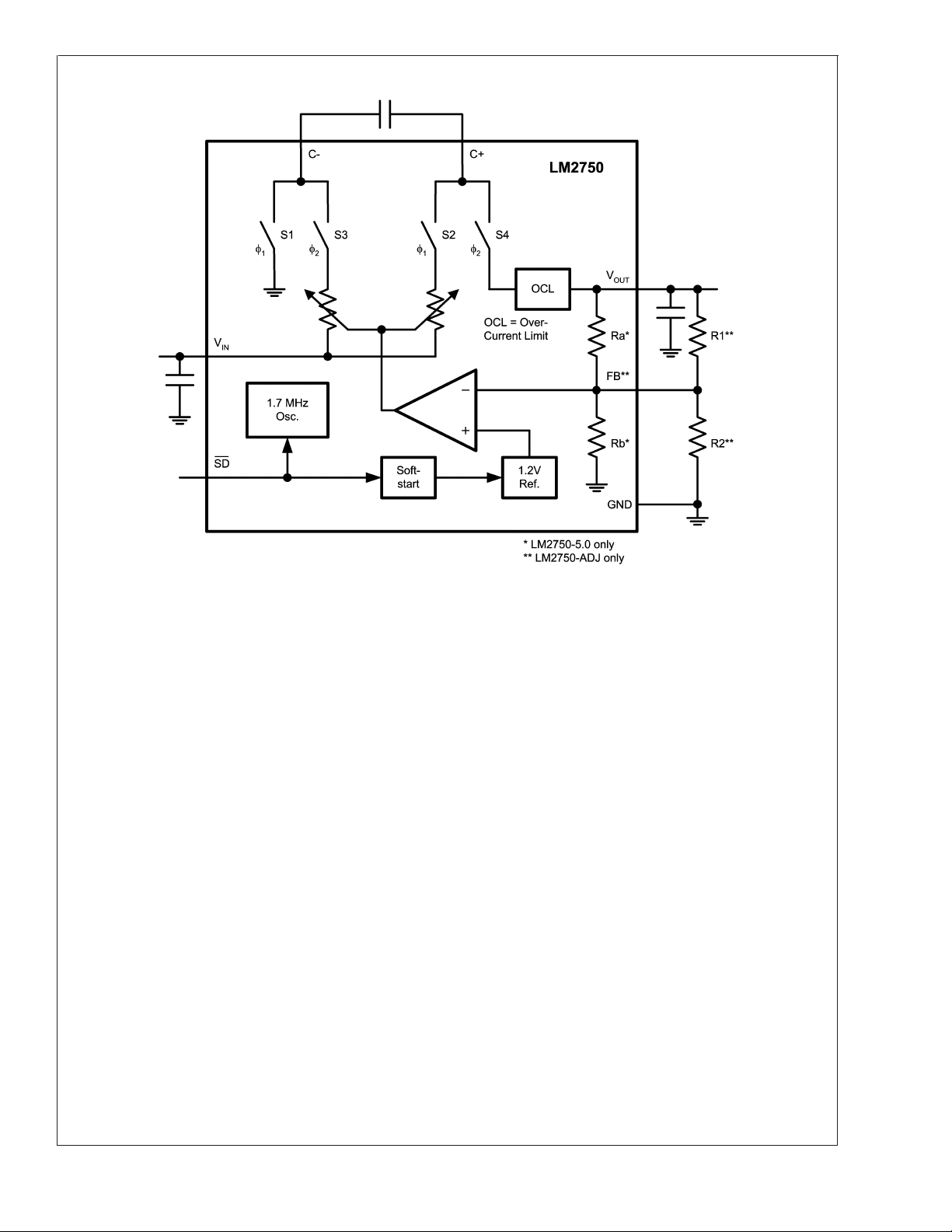
Block Diagram
LM2750
20035103
www.national.com5
Page 6
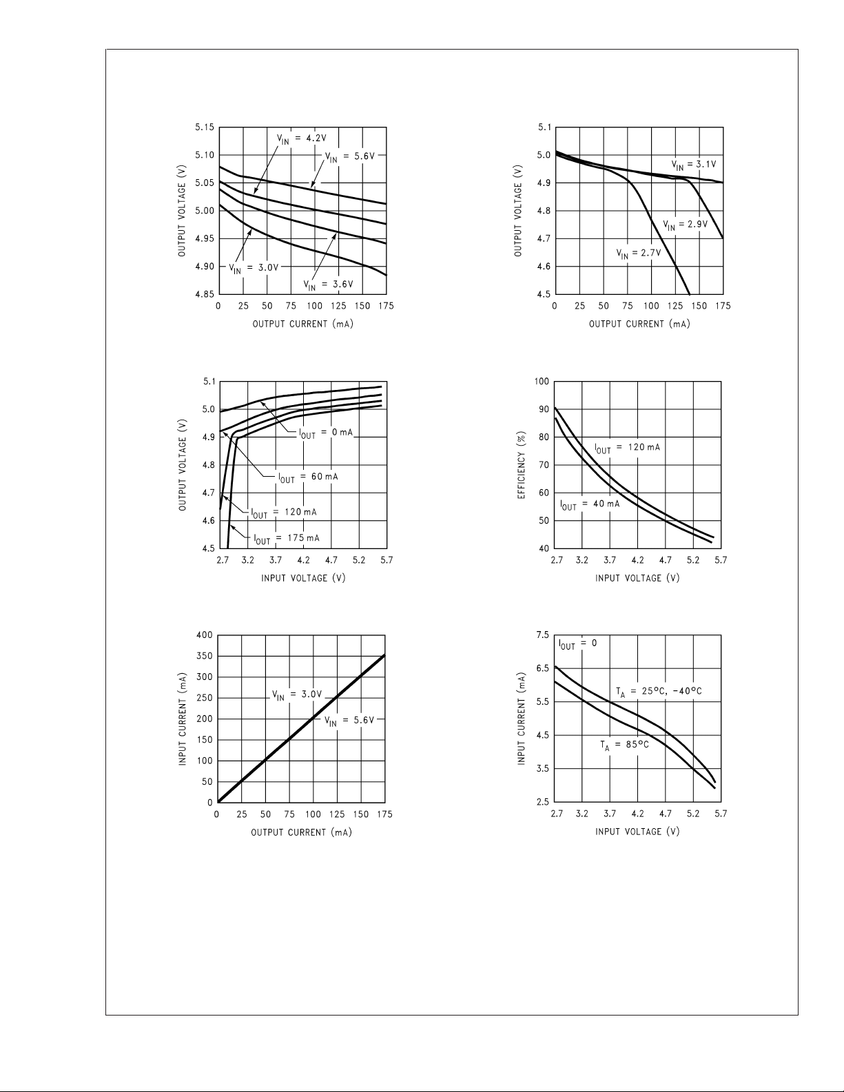
Typical Performance Characteristics Unless otherwise specified: V
2.2µF, C
LM2750
= 1.0µF, C
FLY
Output Voltage vs. Output Current Output Voltage vs. Output Current
Output Voltage vs. Input Voltage Power Efficiency
= 2.2µF. Capacitors are low-ESR multi-layer ceramic capacitors (MLCC’s).
OUT
20035115 20035116
= 3.6V, TA=25oC, CIN=
IN
20035117 20035118
Input Current vs. Output Current Quiescent Supply Current
20035119
20035120
www.national.com 6
Page 7

LM2750
Typical Performance Characteristics Unless otherwise specified: V
2.2µF, C
= 1.0µF, C
FLY
Current Limit Behavior Switching Frequency
Output Voltage Ripple Output Voltage Ripple, I
= 2.2µF. Capacitors are low-ESR multi-layer ceramic capacitors (MLCC’s). (Continued)
OUT
20035121
= 3.6V, TA=25oC, CIN=
IN
20035122
= 120mA
OUT
Turn-on Behavior
20035113
20035112
20035114
www.national.com7
Page 8

Operation Description
LM2750
OVERVIEW
The LM2750 is a regulated switched capacitor doubler that,
by combining the principles of switched-capacitor voltage
boost and linear regulation, generates a regulated output
from an extended Li-Ion input voltage range. A two-phase
non-overlapping clock generated internally controls the operation of the doubler. During the charge phase (φ1), the
flying capacitor (C
ground through internal pass-transistor switches and is
charged to the input voltage. In the pump phase that follows
(φ2), the flying capacitor is connected between the input and
output through similar switches. Stacked atop the input, the
charge of the flying capacitor boosts the output voltage and
supplies the load current.
A traditional switched capacitor doubler operating in this
manner will use switches with very low on-resistance to
generate an output voltage that is 2x the input voltage. The
LM2750 regulates the output voltage by controlling the resistance of the two input-connected pass-transistor switches
in the doubler.
PRE-REGULATION
The very low input current ripple of the LM2750, resulting
from internal pre-regulation, adds very little noise to the input
line. The core of the LM2750 is very similar to that of a basic
switched capacitor doubler: it is composed of four switches
and a flying capacitor (external). Regulation is achieved by
modulating the on-resistance of the two switches connected
to the input pin (one switch in each phase). The regulation is
done before the voltage doubling, giving rise to the term
"pre-regulation". It is pre-regulation that eliminates most of
the input current ripple that is a typical and undesirable
characteristic of a many switched capacitor converters.
INPUT, OUTPUT, AND GROUND CONNECTIONS
Making good input, output, and ground connections is essential to achieve optimal LM2750 performance. The two
input pads, pads 8 and 9, must be connected externally. It is
strongly recommended that the input capacitor (C
placed as close as possible to the LM2750, so that the traces
from the input pads are as short and straight as possible. To
minimize the effect of input noise on LM2750 performance, it
is best to bring two traces out from the LM2750 all the way to
the input capacitor pad, so that they are connected at the
capacitor pad. Connecting the two input traces between the
input capacitor and the LM2750 input pads could make the
LM2750 more susceptible to noise-related performance degradation. It is also recommended that the input capacitor be
on the same side of the PCB as the LM2750, and that traces
remain on this side of the board as well (vias to traces on
other PCB layers are not recommended between the input
capacitor and LM2750 input pads).
The two output pads, pads 1 and 2, must also be connected
externally. It is recommended that the output capacitor
) be placed as close to the LM2750 output pads as
(C
OUT
possible. It is best if routing of output pad traces follow
guidelines similar to those presented for the input pads and
capacitor. The flying capacitor (C
as close to the LM2750 as possible to minimize PCB trace
length between the capacitor and the IC. Due to the padlayout of the part, it is likely that the trace from one of the
flying capacitor pads (C+ or C-) will need to be routed to an
internal or opposite-side layer using vias. This is acceptable,
) is connected between the input and
FLY
) should also be placed
FLY
IN
)be
and it is much more advantageous to route a flying capacitor
trace in this fashion than it is to place input traces on other
layers.
The GND pads of the LM2750 are ground connections and
must be connected externally. These include pads 3
(LM2750-5.0 only), 5, 6 and the die-attach pad (DAP). Large,
low impedance copper fills and via connections to an internal
ground plane are the preferred way of connecting together
the ground pads of the LM2750, the input capacitor, and the
output capacitor, as well as connecting this circuit ground to
the system ground of the PCB.
SHUTDOWN
When the voltage on the active-low-logic shutdown pin is
low, the LM2750 will be in shutdown mode. In shutdown, the
LM2750 draws virtually no supply current. There is a 200kΩ
pull-down resistor tied between the SD pin and GND that
pulls the SD pin voltage low if the pin is not driven by a
voltage source. When pulling the part out of shutdown, the
voltage source connected to the SD pin must be able to drive
the current required by the 200kΩ resistor. For voltage management purposes required upon startup, internal switches
connect the output of the LM2750 to an internal pull-down
resistor (1kΩ typ) when the part is shutdown. Driving the
output of the LM2750 by another supply when the LM2750 is
shutdown is not recommended, as the pull-down resistor
was not sized to sink continuous current.
SOFT START
The LM2750 employs soft start circuitry to prevent excessive
input inrush currents during startup. The output voltage is
programmed to rise from 0V to the nominal output voltage
(5.0V) in 500µs (typ.). Soft-start is engaged when a part, with
input voltage established, is taken out of shutdown mode by
pulling the SD pin voltage high. Soft-start will also engage
when voltage is established simultaneously to the input and
SD pins.
OUTPUT CURRENT CAPABILITY
The LM2750-5.0 is guaranteed to provide 120mA of output
current when the input voltage is within 2.9V-to-5.6V. Using
the LM2750 to drive loads in excess of 120mA is possible.
IMPORTANT NOTE: Understanding relevant application issues is recommended and a thorough analysis of the application circuit should be performed when using the part outside operating ratings and/or specifications to ensure
satisfactory circuit performance in the application. Special
care should be paid to power dissipation and thermal effects.
These parameters can have a dramatic impact on highcurrent applications, especially when the input voltage is
high. (see "Power Efficiency and Power Dissipation" section,
to come).
The schematic of Figure 1 is a simplified model of the
LM2750 that is useful for evaluating output current capability.
The model shows a linear pre-regulation block (Reg), a
voltage doubler (2x), and an output resistance (R
OUT
). Output resistance models the output voltage droop that is inherent to switched capacitor converters. The output resistance
of the LM2750 is 5Ω (typ.), and is approximately equal to
twice the resistance of the four LM2750 switches. When the
output voltage is in regulation, the regulator in the model
controls the voltage V’ to keep the output voltage equal to
±
4%. With increased output current, the voltage drop
5.0V
across R
increases. To prevent droop in output voltage,
OUT
the voltage drop across the regulator is reduced, V’ increases, and V
remains at 5V. When the output current
OUT
www.national.com 8
Page 9

Operation Description (Continued)
increases to the point that there is zero voltage drop across
the regulator, V’ equals the input voltage, and the output
voltage is "on the edge" of regulation. Additional output
current causes the output voltage to fall out of regulation,
and the LM2750 operation is similar to a basic open-loop
doubler. As in a voltage doubler, increase in output current
results in output voltage drop proportional to the output
resistance of the doubler. The out-of-regulation LM2750 output voltage can be approximated by:
= 2xVIN-I
V
OUT
Again, this equation only applies at low input voltage and
high output current where the LM2750 is not regulating. See
Output Current vs. Output Voltage curves in the Typical
Performance Characteristics section for more details.
OUTxROUT
switches into shutdown mode. The LM2750 releases thermal
shutdown when the junction temperature of the part is reduced to 130
o
C (typ.).
Thermal shutdown is most-often triggered by self-heating,
which occurs when there is excessive power dissipation in
the device and/or insufficient thermal dissipation. LM2750
power dissipation increases with increased output current
and input voltage (see Power Efficiency and Power Dissi-
pation section). When self-heating brings on thermal shutdown, thermal cycling is the typical result. Thermal cycling is
the repeating process where the part self-heats, enters thermal shutdown (where internal power dissipation is practically
zero), cools, turns-on, and then heats up again to the thermal shutdown threshold. Thermal cycling is recognized by a
pulsing output voltage and can be stopped be reducing the
internal power dissipation (reduce input voltage and/or output current) or the ambient temperature. If thermal cycling
occurs under desired operating conditions, thermal dissipation performance must be improved to accommodate the
power dissipation of the LM2750. Fortunately, the LLP package has excellent thermal properties that, when soldered to
a PCB designed to aid thermal dissipation, allows the
LM2750 to operate under very demanding power dissipation
conditions.
LM2750
20035109
FIGURE 1. LM2750 Output Resistance Model
A more complete calculation of output resistance takes into
account the effects of switching frequency, flying capacitance, and capacitor equivalent series resistance (ESR).
This equation is shown below:
Switch resistance (5Ω typ.) dominates the output resistance
equation of the LM2750. With a 1.7MHz typical switching
frequency, the 1/(FxC) component of the output resistance
contributes only 0.6Ω to the total output resistance. Increasing the flying capacitance will only provide minimal improvement to the total output current capability of the LM2750. In
some applications it may be desirable to reduce the value of
the flying capacitor below 1µF to reduce solution size and/or
cost, but this should be done with care so that output resistance does not increase to the point that undesired output
voltage droop results. If ceramic capacitors are used, ESR
will be a negligible factor in the total output resistance, as the
ESR of quality ceramic capacitors is typically much less than
100mΩ.
THERMAL SHUTDOWN
The LM2750 implements a thermal shutdown mechanism to
protect the device from damage due to overheating. When
the junction temperature rises to 150
o
C (typ.), the part
OUTPUT CURRENT LIMITING
The LM2750 contains current limit circuitry that protects the
device in the event of excessive output current and/or output
shorts to ground. Current is limited to 300mA (typ.) when the
output is shorted directly to ground. When the LM2750 is
current limiting, power dissipation in the device is likely to be
quite high. In this event, thermal cycling should be expected
(see Thermal Shutdown section).
PROGRAMMING THE OUTPUT VOLTAGE OF THE LM2750-ADJ
As shown in the application circuit of Figure 2, the output
voltage of the LM2750-ADJ can be programmed with a
simple resistor divider (see resistors R1 and R2). The values
of the feedback resistors set the output voltage, as determined by the following equation:
= 1.23V x (1 + R1/ R2)
V
OUT
In the equation above, the "1.23V" term is the nominal
voltage of the feedback pin when the feedback loop is correctly established and the part is operating normally. The
sum of the resistance of the two feedback resistors should
be between 15kΩ and 20kΩ:
<
15kΩ
(R1 + R2)<20kΩ
If larger feedback resistors are desired, a 10pF capacitor
should be placed in parallel with resistor R1.
www.national.com9
Page 10

Operation Description (Continued)
LM2750
FIGURE 2. LM2750-ADJ Typical Application Circuit
20035123
Application Information
OUTPUT VOLTAGE RIPPLE
The amount of voltage ripple on the output of the LM2750 is
highly dependent on the application conditions: output current and the output capacitor, specifically. A simple approximation of output ripple is determined by calculating the
amount of voltage droop that occurs when the output of the
LM2750 is not being driven. This occurs during the charge
phase (φ1). During this time, the load is driven solely by the
charge on the output capacitor. The magnitude of the ripple
thus follows the basic discharge equation for a capacitor (I =
C x dV/dt), where discharge time is one-half the switching
period, or 0.5/F
A more thorough and accurate examination of factors that
affect ripple requires including effects of phase non-overlap
times and output capacitor equivalent series resistance
(ESR). In order for the LM2750 to operate properly, the two
phases of operation must never coincide. (If this were to
happen all switches would be closed simultaneously, shorting input, output, and ground). Thus, non-overlap time is built
into the clocks that control the phases. Since the output is
not being driven during the non-overlap time, this time
should be accounted for in calculating ripple. Actual output
capacitor discharge time is approximately 60% of a switching period, or 0.6/F
The ESR of the output capacitor also contributes to the
output voltage ripple, as there is effectively an AC voltage
drop across the ESR due to current switching in and out of
the capacitor. The following equation is a more complete
calculation of output ripple than presented previously, taking
into account phase non-overlap time and capacitor ESR.
. Put simply,
SW
.
SW
A low-ESR ceramic capacitor is recommended on the output
to keep output voltage ripple low. Placing multiple capacitors
in parallel can reduce ripple significantly, both by increasing
capacitance and reducing ESR. When capacitors are in
parallel, ESR is in parallel as well. The effective net ESR is
determined according to the properties of parallel resistance.
Two identical capacitors in parallel have twice the capacitance and half the ESR as compared to a single capacitor of
the same make. On a similar note, if a large-value, high-ESR
capacitor (tantalum, for example) is to be used as the primary output capacitor, the net output ESR can be significantly reduced by placing a low-ESR ceramic capacitor in
parallel with this primary output capacitor.
CAPACITORS
The LM2750 requires 3 external capacitors for proper operation. Surface-mount multi-layer ceramic capacitors are recommended. These capacitors are small, inexpensive and
have very low equivalent series resistance (≤10mΩ typ.).
Tantalum capacitors, OS-CON capacitors, and aluminum
electrolytic capacitors generally are not recommended for
use with the LM2750 due to their high ESR, as compared to
ceramic capacitors.
For most applications, ceramic capacitors with X7R or X5R
temperature characteristic are preferred for use with the
LM2750. These capacitors have tight capacitance tolerance
±
(as good as
±
15% over -55oCto125oC; X5R:±15% over -55oCto85oC),
10%), hold their value over temperature (X7R:
and typically have little voltage coefficient. Capacitors with
Y5V and/or Z5U temperature characteristic are generally not
recommended. These types of capacitors typically have
wide capacitance tolerance (+80%, -20%), vary significantly
over temperature (Y5V: +22%, -82% over -30
range; Z5U: +22%, -56% over +10
o
Cto+85oC range), and
o
Cto+85oC
have poor voltage coefficients. Under some conditions, a
nominal 1µF Y5V or Z5U capacitor could have a capacitance
of only 0.1µF. Such detrimental deviation is likely to cause
these Y5V and Z5U of capacitors to fail to meet the minimum
capacitance requirements of the LM2750.
The table below lists some leading ceramic capacitor manufacturers.
www.national.com 10
Page 11

Application Information (Continued)
Manufacturer Contact Information
TDK www.component.tdk.com
AVX www.avx.com
Murata www.murata.com
Taiyo-Yuden www.t-yuden.com
Vishay-Vitramon www.vishay.com
INPUT CAPACITOR
The input capacitor (C
helping to quickly transfer charge to the flying capacitor
during the charge phase (φ1) of operation. The input capacitor helps to keep the input voltage from drooping at the start
of the charge phase, when the flying capacitor is first connected to the input, and helps to filter noise on the input pin
that could adversely affect sensitive internal analog circuitry
biased off the input line. As mentioned above, an X7R/X5R
ceramic capacitor is recommended for use. For applications
where the maximum load current required is between 60mA
and 120mA, a minimum input capacitance of 2.0µF is required. For applications where the maximum load current is
60mA or less, 1.0µF of input capacitance is sufficient. Failure
to provide enough capacitance on the LM2750 input can
result in poor part performance, often consisting of output
voltage droop, excessive output voltage ripple and/or excessive input voltage ripple.
A minimum voltage rating of 10V is recommended for the
input capacitor. This is to account for DC bias properties of
ceramic capacitors. Capacitance of ceramic capacitors reduces with increased DC bias. This degradation can be quite
>
significant (
50%) when the DC bias approaches the volt-
age rating of the capacitor.
FLYING CAPACITOR
The flying capacitor (C
the output, providing the voltage boost of the doubler. A
polarized capacitor (tantalum, aluminum electrolytic, etc.)
must not be used here, as the capacitor will be reversebiased upon start-up of the LM2750. The size of the flying
capacitor and its ESR affect output current capability when
the input voltage of the LM2750 is low, most notable for input
voltages below 3.0V. These issues were discussed previously in the Output Current Capability section. For most
applications, a 1µF X7R/X5R ceramic capacitor is recommended for the flying capacitor.
OUTPUT CAPACITOR
The output capacitor of the LM2750 plays an important part
in determining the characteristics of the output signal of the
LM2750, many of which have already been discussed. The
ESR of the output capacitor affects charge pump output
resistance, which plays a role in determining output current
capability. Both output capacitance and ESR affect output
voltage ripple. For these reasons, a low-ESR X7R/X5R ceramic capacitor is the capacitor of choice for the LM2750
output.
In addition to these issues previously discussed, the output
capacitor of the LM2750 also affects control-loop stability of
the part. Instability typically results in the switching frequency effectively reducing by a factor of two, giving excessive output voltage droop and/or increased voltage ripple on
the output and the input. With output currents of 60mA or
less, a minimum capacitance of 1.0µF is required at the
) is used as a reservoir of charge,
IN
) transfers charge from the input to
FLY
output to ensure stability. For output currents between 60mA
and 120mA, a minimum output capacitance of 2.0µF is
required.
A minimum voltage rating of 10V is recommended for the
output capacitor. This is to account for DC bias properties of
ceramic capacitors. Capacitance of ceramic capacitors reduces with increased DC bias. This degradation can be quite
>
significant (
50%) when the DC bias approaches the volt-
age rating of the capacitor.
POWER EFFICIENCY AND POWER DISSIPATION
Efficiency of the LM2750 mirrors that of an unregulated
switched capacitor converter followed by a linear regulator.
The simplified power model of the LM2750, in Figure 3, will
be used to discuss power efficiency and power dissipation.
In calculating power efficiency, output power (P
OUT
) is easily
determined as the product of the output current and the 5.0V
output voltage. Like output current, input voltage is an
application-dependent variable. The input current can be
calculated using the principles of linear regulation and
switched capacitor conversion. In an ideal linear regulator,
the current into the circuit is equal to the current out of the
circuit. The principles of power conservation mandate the
ideal input current of a voltage doubler must be twice the
output current. Adding a correction factor for operating quiescent current (I
, 5mA typ.) gives an approximation for total
Q
input current which, when combined with the other input and
output parameter(s), yields the following equation for efficiency:
Comparisons of LM2750 efficiency measurements to calculations using the above equation have shown the equation to
be a quite accurate approximation of actual efficiency. Because efficiency is inversely proportional to input voltage, it
is highest when the input voltage is low. In fact, for an input
voltage of 2.9V, efficiency of the LM2750 is greater than 80%
≥ 40mA) and peak efficiency is 85% (I
(I
OUT
OUT
= 120mA).
The average efficiency for an input voltage range spanning
the Li-Ion range (2.9V-to-4.2V) is 70% (I
= 120mA). At
OUT
higher input voltages, efficiency drops dramatically. In Li-Ionpowered applications, this is typically not a major concern,
as the circuit will be powered off a charger in these circumstances. Low efficiency equates to high power dissipation,
however, which could become an issue worthy of attention.
LM2750 power dissipation (P
) is calculated simply by sub-
D
tracting output power from input power:
P
D=PIN-POUT
=[VINx (2·I
OUT+IQ
)]-[V
OUTxIOUT
]
Power dissipation increases with increased input voltage
and output current, up to 772mW at the ends of the operating
ratings (V
= 5.6V, I
IN
= 120mA). Internal power dissipa-
OUT
tion self-heats the device. Dissipating this amount power/
heat so the LM2750 does not overheat is a demanding
thermal requirement for a small surface-mount package.
When soldered to a PCB with layout conducive to power
dissipation, the excellent thermal properties of the LLP package enable this power to be dissipated from the LM2750 with
little or no derating, even when the circuit is placed in elevated ambient temperatures.
LM2750
www.national.com11
Page 12

Application Information (Continued)
LM2750
FIGURE 3. LM2750 Model for Power Efficiency and
Power Dissipation Calculations
LAYOUT RECOMMENDATIONS
A good board layout of the LM2750 circuit is required to
achieve optimal assembly, electical, and thermal dissipation
perfromance. Figure 4 is an example of a board layout
20035110
implementing recommended techniques. For more information related to layout for the LLP package, refer to National
Semiconductor’s Application Note 1187: Leadless Lead-
frame Package (LLP). Below are some general guidelines
for board layout:
Place capacitors as close to the as possible to the
•
LM2750, and on the same side of the board. V
connections are most critical: run short traces from
V
OUT
and
IN
the LM2750 pads directly to these capacitor pads.
Connect the ground pins of the LM2750 and the capaci-
•
tors to a good ground plane. The ground plane is essential for both electrical and thermal disspation performance.
For optimal thermal performance, make the ground
•
plane(s) as large as possible. Connect the die-attach pad
(DAP) of the LM2750 to the ground plane(s) with wide
traces and/or multiple vias. Top-layer ground planes are
most effective in increasing the thermal dissipation capability of the LLP package. Large internal ground planes
are also very effective in keeping the die temperature of
the LM2750 within operating ratings.
20035126
FIGURE 4. LM2750-5.0 Recommended Layout
www.national.com 12
Page 13

LM2750 LED Drive Application
FIGURE 5. LM2750-5.0 LED Drive Application Circuit
LM2750
20035124
FIGURE 6. LM2750-ADJ LED Drive Application Circuit
The LM2750 is an excellent part for driving white and blue
LEDs for display backlighting and other general-purpose
lighting functions. The circuits of Figure 5 and Figure 6 show
LED driver circuits for the LM2750-5.0 and the LM2750-ADJ,
respectively. Simply placing a resistor (R) in series with each
LED sets the current through the LEDs:
=(V
I
LED
OUT-VLED
In the equation above, I
a particular LED, and V
)/R
is the current that flows through
LED
is the forward voltage of the LED
LED
at the given current. As can be seen in the equation above,
LED current will vary with changes in LED forward voltage
). Mismatch of LED currents will result in brightness
(V
LED
mismatch from one LED to the next.
The feedback pin of the LM2750-ADJ can be utilized to help
better control brightness levels and negate the effects of
LED forward voltage variation. As shown in Figure 6, connecting the feedback pin to the primary LED-resistor junction
(LED1-R1) regulates the current through that LED. The voltage across the primary resistor (R1) is the feedback pin
20035125
voltage (1.23V typ.), and the current through the LED is the
current through that resistor. Current through all other LEDs
(LEDx) will not be regulated, however, and will vary with LED
forward voltage variations. When using the LM2750-ADJ in
current-mode, LED currents can be calculated with the
equations below:
= 1.23V / R1
I
LED1
I
LEDx
= (1.23V + V
LED1-VLEDx
)/Rx
The current-mode configuration does not improve brightness
matching from one LED to another in a single circuit, but will
keep currents similar from one circuit to the next. For example: if there is forward voltage mismatch from LED1 to
LED2 on a single board, the current-mode LM2750-ADJ
solution provides no benefit. But if the forward voltage of
LED1 on one board is different than the forward voltage of
LED1 on another board, the currents through LED1 in both
phones will match. THis helps keep LED currents fairly
consistent from one product to the next, adn helps to offset
lot-to-lot variation of LED forward voltage characteristics.
www.national.com13
Page 14

LM2750 LED Drive Application
(Continued)
LM2750
PWM BRIGHTNESS/DIMMING CONTROL
Brightness of the LEDs can be adjusted in an application by
driving the SD pin of the LM2750 with a PWM signal. When
the PWM signal is high, the LM2750 is ON, and current flows
through the LEDs, as described in the previous section. A
low PWM signal turns the part and the LEDs OFF. The
perceived brightness of the LEDs is proportional to ON
current of the LEDs and the duty cycle (D) of the PWM signal
(the percentage of time the LEDs are ON).
To achieve good brightness/dimming control with this circuit,
proper selection of the PWM frequency is required. The
PWM frequency (F
avoid visible flickering of the LED light. An upper bound on
this frequency is also needed to accomodate the turn-on
time of the LM2750 (T
recommended PWM frequency is similarly dependent on the
minimum duty cycle (D
equation puts bounds on the reommended PWM frequency
range:
100Hz
Choosing a PWM frequency within these limits will result in
fairly linear control of the time-averaged LED current over
the full duty-cycle adjustment range. For most applications, a
PWM frequency between 100Hz and 500Hz is recommended. A PWM frequency up to 1kHz may be acceptable in
some designs.
LED DRIVER POWER EFFICIENCY
Efficiency of an LED driver (E
power consumed by the LEDs (P
consumed at the input of the circuit. Input power consumption of the LM2750 was explained and defined in the previous section titled: Power Efficiency and Power Dissipa-
tion. Assuming LED forward voltages and currents match
reasonably well, LED power consumption is the product of
the number of LEDs in the circuit (N), the LED forward
voltage (V
P
LED
E
LED=PLED/PIN
), and the LED forward current (I
LED
=NxV
LEDxILED
Figure 7 is an efficiency curve for a typical LM2750 LEDdrive application.
) should be set higher than 100Hz to
PWM
= 0.5ms typ.). This maximum
ON
) of the application. The following
MIN
<
= (NxV
F
PWM
LED
LEDxILED
<
D
MIN÷TON
) is typically defined as the
) divided by the power
LED
)/{VINx [(2xI
LED
OUT
):
) + 5mA]}
LED DRIVER POWER CONSUMPTION
For battery-powered LED-drive applications, it is strongly
recommended that power consumption, rather than power
efficiency, be used as the metric of choice when evaluating
power conversion performance. Power consumed (P
simply the product of input voltage (V
):
(I
IN
P
IN=VINxIIN
) and input current
IN
IN
)is
LM2750 input current is equal to twice the output current
), plus the supply current of the part (nominally 5mA):
(I
OUT
I
IN
= (2xI
OUT
) + 5mA
Output voltage and LED voltage do not impact the amount of
current consumed by the LM2750 circuit. Thus, neither factor
affects the current draw on a battery. Since output voltage
does not impact input current, there is no power savings with
either the LM2750-5.0 or the LM2750-ADJ: both options
consume the same amount of power.
In the previous section, LED Driver Efficiency was defined
as:
E
LED=PLED/PIN
= (NxV
LEDxILED
)/{VINx [(2xI
OUT
) + 5mA]}
The equation above can be simplified by recognizing the
following:
>>
2xI
NxI
OUT
LED=IOUT
5mA (high output current applications)
Simplification yields:
E
LED=VLED/VIN
This is in direct contrast to the previous assertion that
showed that power consumption was completely independent of LED voltage. As is the case here with the LM2750,
efficiency is often not a good measure of power conversion
effectiveness of LED driver topologies. This is why it is
strongly recommended that power consumption be studied
or measured when comparing the power conversion effictiveness of LED drivers.
One final note: efficiency of an LED drive solution should not
be confused with an efficiency calculation for a standard
power converter (E
E
P=POUT/PIN
).
P
=(V
OUTxIOUT
)/(VINxIIN)
The equation above neglects power losses in the external
resistors that set LED currents and is a very poor metric of
LED-drive power conversion performance.
20035127
FIGURE 7. LM2750 LED Drive Efficiency. 6 LEDs, I
20mA each, V
www.national.com 14
LED
= 4.0V
LED
=
Page 15

Datasheet Revision History
REV. # DATE COMMENTS
1.0 Production Release of LM2750 Datasheet
1.1 09/24/2004 Preliminary version with the following additions:
SDA10A Non-pullback package Added (pgs 2, 16)
•
Absolute Maximum Output Current Rating Added (pgs 3, 4)
•
1.2 09/28/2005 Production Release of new LM2750 Datasheet
Ordering information for SDA10A package added
•
Reference to SDA10A package option added to the Connection Diagram
•
section
1.3 12/21/2005 Production release of new Datasheet for ADJ voltage option in the
No-Pullback Package
Physical Dimensions inches (millimeters) unless otherwise noted
LM2750
10-Pin Pullback LLP
NS Package Number LDA10A
www.national.com15
Page 16

Physical Dimensions inches (millimeters) unless otherwise noted (Continued)
10-Pin Non-Pullback LLP
NS Package Number SDA10A
LM2750 Low Noise Switched Capacitor Boost Regulator
National does not assume any responsibility for use of any circuitry described, no circuit patent licenses are implied and National reserves
the right at any time without notice to change said circuitry and specifications.
For the most current product information visit us at www.national.com.
LIFE SUPPORT POLICY
NATIONAL’S PRODUCTS ARE NOT AUTHORIZED FOR USE AS CRITICAL COMPONENTS IN LIFE SUPPORT DEVICES OR SYSTEMS
WITHOUT THE EXPRESS WRITTEN APPROVAL OF THE PRESIDENT AND GENERAL COUNSEL OF NATIONAL SEMICONDUCTOR
CORPORATION. As used herein:
1. Life support devices or systems are devices or systems
which, (a) are intended for surgical implant into the body, or
(b) support or sustain life, and whose failure to perform when
properly used in accordance with instructions for use
provided in the labeling, can be reasonably expected to result
in a significant injury to the user.
BANNED SUBSTANCE COMPLIANCE
National Semiconductor manufactures products and uses packing materials that meet the provisions of the Customer Products
Stewardship Specification (CSP-9-111C2) and the Banned Substances and Materials of Interest Specification (CSP-9-111S2) and contain
no ‘‘Banned Substances’’ as defined in CSP-9-111S2.
Leadfree products are RoHS compliant.
National Semiconductor
Americas Customer
Support Center
Email: new.feedback@nsc.com
Tel: 1-800-272-9959
www.national.com
National Semiconductor
Europe Customer Support Center
Fax: +49 (0) 180-530 85 86
Email: europe.support@nsc.com
Deutsch Tel: +49 (0) 69 9508 6208
English Tel: +44 (0) 870 24 0 2171
Français Tel: +33 (0) 1 41 91 8790
2. A critical component is any component of a life support
device or system whose failure to perform can be reasonably
expected to cause the failure of the life support device or
system, or to affect its safety or effectiveness.
National Semiconductor
Asia Pacific Customer
Support Center
Email: ap.support@nsc.com
National Semiconductor
Japan Customer Support Center
Fax: 81-3-5639-7507
Email: jpn.feedback@nsc.com
Tel: 81-3-5639-7560
Page 17

 Loading...