

Page 1
LM2685
Dual Output Regulated Switched Capacitor Voltage
Converter
LM2685 Dual Output Regulated Switched Capacitor Voltage Converter
May 2000
General Description
The LM2685 CMOS charge-pump voltage converter operates as an input voltage doubler, +5V regulator and inverter
for aninput voltage in the range of +2.85V to +6.5V. Five low
cost capacitors are used in this circuit to provide up to 50mA
of output current at +5V (
LM2685 operates at a 130 kHz switching frequency to reduce output resistance and voltage ripple. With an operating
current of only 800µA (operating efficiency greater than 80%
with most loads) and 6µA typical shutdown current, the
LM2685 is ideal for use in battery powered systems. The device is in a small 14-pin TSSOP package.
±
5%), and 15mA at −5V. The
Features
n +5V regulated output
n Inverts V
n Doubles input supply voltage
n TSSOP-14 package
n 80% typical conversion efficiency at 25mA
n Input voltage range of 2.85V to 6.5V
n Independent shutdown control pins
Applications
n Cellular phones
n Pagers
n PDAs
n Handheld instrumentation
n 3.3V to 5V voltage conversion applications
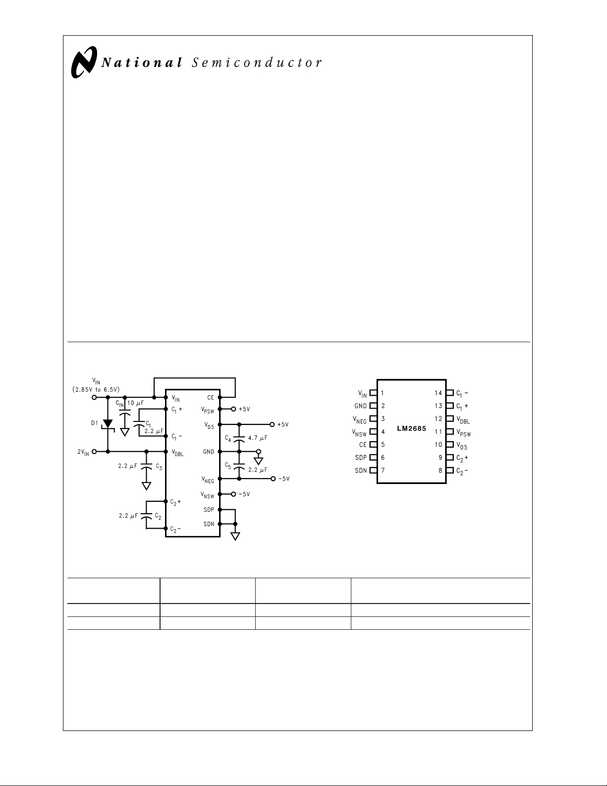
Typical Application and Connection Diagram
(+5V) to V
05
NEG
(−5V)
DS101100-2
14-Pin TSSOP
DS101100-1
Ordering Information
Order Number Package Type
LM2685MTC TSSOP-14 MTC14 94 Units, Rail
LM2685MTCX TSSOP-14 MTC14 2.5k Units, Tape and Reel
© 2000 National Semiconductor Corporation DS101100 www.national.com
NSC Package
Drawing
Supplied As
Page 2
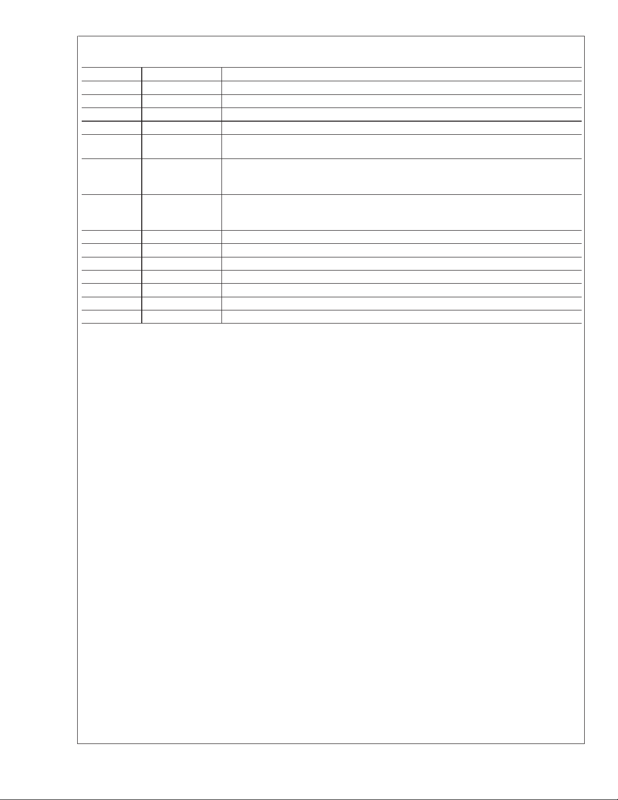
Pin Description
LM2685
Pin No. Name Function
1V
IN
2 GND Power supply ground.
3V
4V
NEG
NSW
5 CE Chip enable input. This pin is high for normal operation and low for shutdown. (See
6 SDP Positive side shutdown input. This pin is low for normal operation and high for positive
7 SDN Negative side shutdown input. This pin is low for normal operation and high for negative
8C
9C
10 V
11 V
12 V
13 C
14 C
−
2
+
2
05
PSW
DBL
+
1
−
1
Power supply input voltage.
Negative output voltage created by inverting V05.
V
output connected through a series switch, NSW.
NEG
Shutdown and Load Disconnect section in the Detailed Device Description division).
side shutdown and V
load disconnect. (See Shutdown and Load Disconnect section
PSW
in the Detailed Device Description division).
side shutdown and V
load disconnect. (See Shutdown and Load Disconnect section
NSW
in the Detailed Device Description division).
The negative terminal of inverting charge-pump capacitor, C2.
The positive terminal of inverting charge-pump capacitor, C2.
Regulated +5V output.
V05output connected through a series switch, PSW.
Voltage Doubler Output. (2.85V ≤ VIN≤ 5.4V. See Voltage Doubler section).
The positive terminal of doubling charge-pump capacitor, C1.
The negative terminal of doubling charge-pump capacitor, C1.
www.national.com 2
Page 3
LM2685
Absolute Maximum Ratings (Note 1)
If Military/Aerospace specified devices are required,
please contact the National Semiconductor Sales Office/
Distributors for availability and specifications.
Supply Voltage (V
GND to V
NEG
SDN, SDP, CE (GND − 0.3V) to
V
Continuous Output Current 80mA
05
V
Short-Circuit Duration to GND
05
to GND or
IN
) 6.8V
(V
+ 0.3V)
IN
Continuous Power Dissipation (T
A
= 25˚C) (Note 3) 600mW
T
(Note 3) 150˚C
JMAX
θ
(Note 3) 140˚C/W
JA
Operating Ambient Temp. Range −40˚C to 85˚C
Operating Junction Temp. Range −40˚C to 125˚C
Storage Temp. Range −65˚C to 150˚C
Lead Temp. (Soldering, 10 sec.) 300˚C
ESD Rating (Note 4) 2kV
(Note 2) Indefinite
Electrical Characteristics
Limits with standard typeface apply for TJ= 25˚C, and limits in boldface type apply over the full temperature range. Unless
otherwise specified V
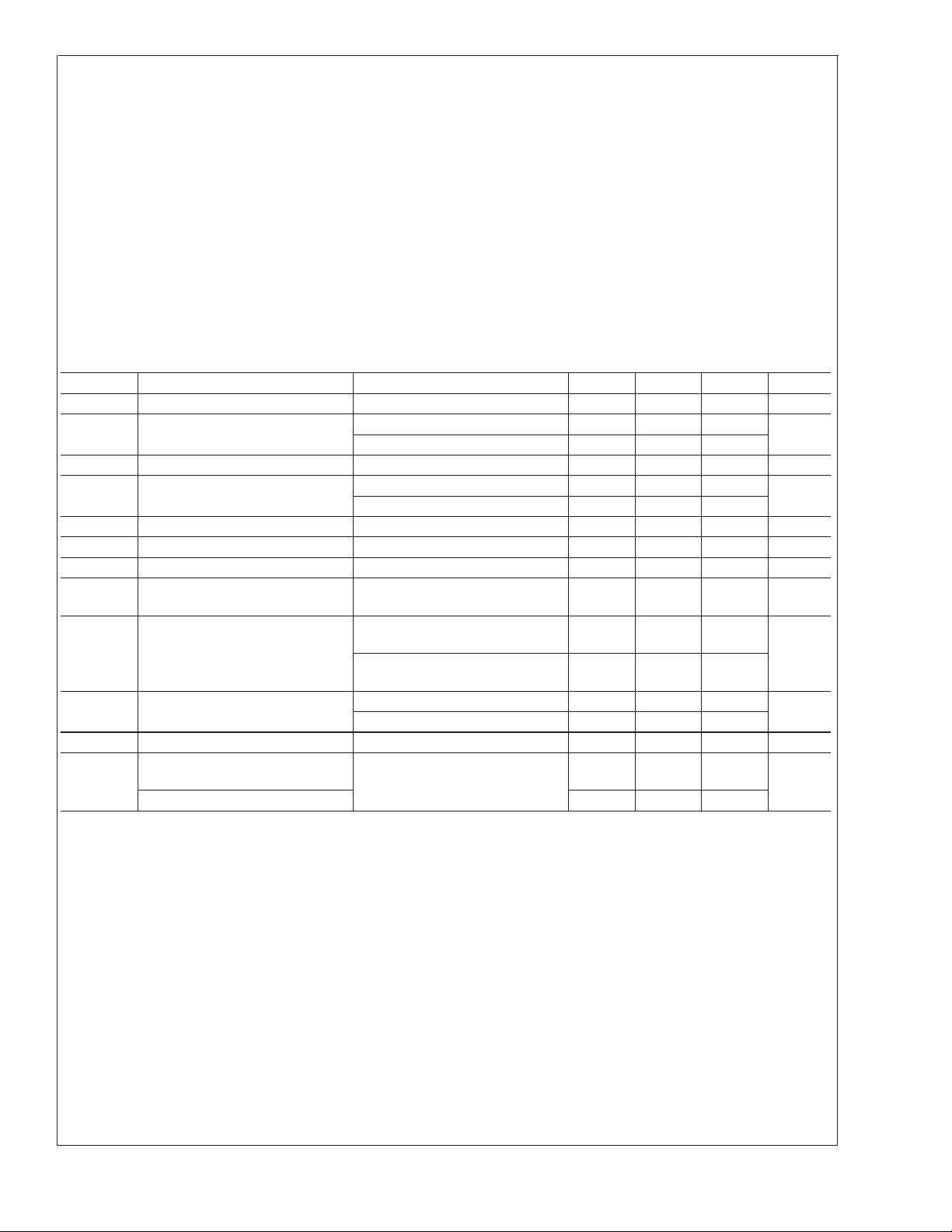
Symbol Parameter Conditions Min Typ Max Units
+
V
I
Q
I
SD
V
SD
Supply Voltage 2.85 6.5 V
Supply Current No Load 800 1600
Shutdown Supply Current VIN= 6.5V 6 30 µA
Shutdown Pin Input Voltage for
CE, SDP, SDN
I
(+5V) Output Current at V
L
R
(−5V) Output Resistance at V
O
F
SW
P
EFF
V
05
G
LINE
G
LOAD
R
SW
Note 1: Absolute Maximum Ratings indicate limits beyond which damage to the device may occur. Operating Ratings indicate conditions for which the device is intended to be functional, but do not guarantee specific performance limits. For guaranteed specifications and test conditions, see the Electrical Characteristics.
Note 2: V
85˚C, V
Note 3: The maximum allowable power dissipation is calculated by using P
ambient temperature and θ
Note 4: The human body model is a 100 pF capacitor discharged through a 1.5kΩ resistor into each pin.
Note 5: In the typical operating circuit, capacitors C
reduce output voltage and efficiency.
Note 6: Specified output resistance includes internal switch resistance and ESR of capacitors. See the Detailed Device Description section.
Note 7: The 50 mA maximum current assumes no current is drawn from V
Switch Frequency 85 130 180 kHz
Average Power Efficiency at V
Output Regulation 1mA<I
Line Regulation 2.85V<V
Load Regulation 1mA<I
Series Switch Resistance V
V
NSW
V
05
may be shorted to GND without damage. However, shorting V
05
must not be shorted to GND or device may be damaged.
05
= 3.6V, C1=C2=C3=C5= 2.2µF. C4= 4.7µF (Note 5)
IN
No Load, V
= 6.5V 300 600
IN
05
NEG
2.85V<V
IL= 15mA (Note 6) 20 40 Ω
2.85V ≤ VIN≤ 6.5V
05
= 25mA to GND
I
L
<
6.5V 50 mA
IN
<
50mA, VIN= 6.5V
L
(Note 7)
<
1mA
<
I
50mA, VIN= 6.5V
L
(Note 7)
<
3.6V 0.25
IN
<
<
V
3.6V
to
NEG
to V
PSW
is the junction-to-ambient thermal resistance of the specified package.
JA
and C2are 2.2µF,0.3ΩmaximumESR capacitors. Capacitors with higher ESR will increase output resistance,
1
>
V
IN
6.5V 0.05
IN
<
50mA, VIN= 6.5V 0.3 1.0 %
L
2.85V 1.5
to V05may damage the device and must be avoided. Also, for temperature above
NEG
=(T
DMAX
pin. See Voltage Doubler section in the Detailed Device Description.
DBL
@
6.5V 0.8
82 %
4.848 5.05 5.252
4.797 5.05 5.303
5.0
JMAX—TA
)/θJA, where T
is the maximum junction temperature, TAis the
JMAX
µA
V
V
%/V
Ω
www.national.com3
Page 4
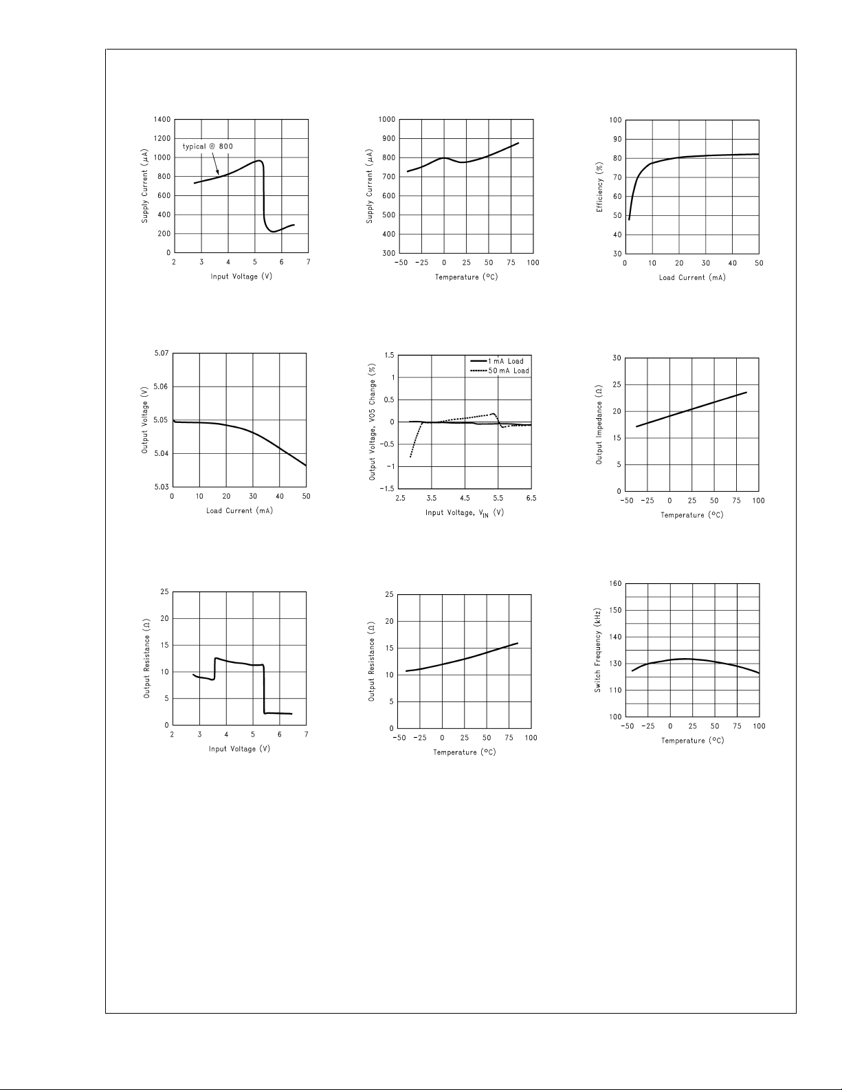
Typical Performance Characteristics Unless otherwise specified, T
LM2685
Supply Current vs Input Voltage
Supply Current vs Temperature
= 25˚C, VIN= 3.6V.
A
Efficiency vs Load Current
DS101100-6
Output Voltage (V05) vs.
Load Current
DS101100-9
Output Resistance (VDBL) vs.
Input Voltage
DS101100-7
V05Voltage vs.
Input Voltage
DS101100-21
Output Resistance (VDBL) vs.
Temperature
DS101100-8
Output Resistance (VNEG) vs.
Temperature
DS101100-10
Switch Frequency vs. Temperature
DS101100-11
www.national.com 4
DS101100-12
DS101100-13
Page 5
LM2685
Typical Performance Characteristics Unless otherwise specified, T
3.6V. (Continued)
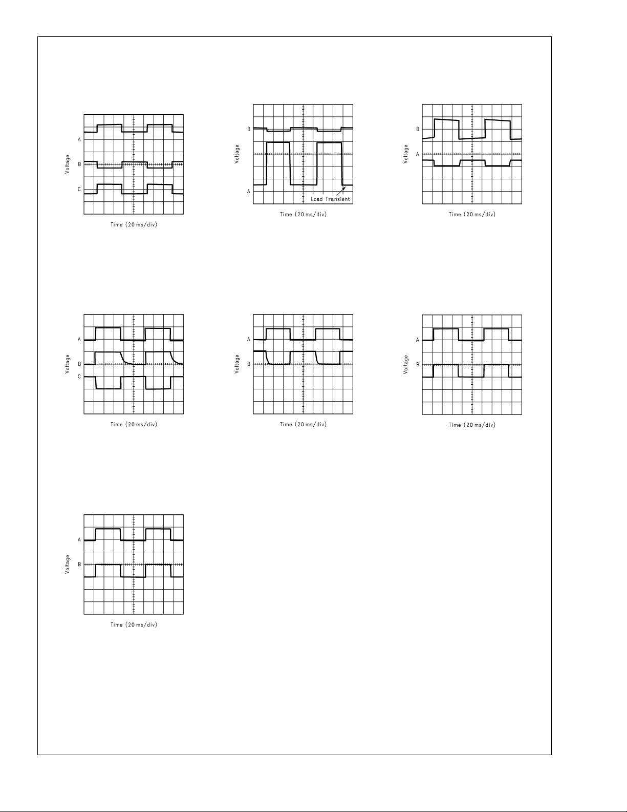
Line Transient Response (with 5mA
Load)
DS101100-14
A: INPUT VOLTAGE: VIN= 3.2V to 6.0V, 5V/div
B: OUTPUT VOLTAGE: V
C: OUTPUT VOLTAGE: V
V
and V
PSW
NSW
: 100mV/div
PSW
: 100mV/div
NSW
Response to CE
(with 5mA Load)
V05Load Transient Response
DS101100-15
A: LOAD CURRENT: I
10mA/div
B: OUTPUT VOLTAGE: V
= 5mA to 39.6mA,
LOAD
: 10mV/div
05
V05Response to SDP (with 5mA
Load)
V
A: LOAD CURRENT: I
10mA/div
B: OUTPUT VOLTAGE: V
V
Load)
= 25˚C, VIN=
A
Load Transient Response
NSW
= 4.4mA to −9.4mA,
LOAD
: 50mV/div
NSW
Response to SDP (with 5mA
NSW
DS101100-16
A: CE INPUT: 5V/div
B: OUTPUT VOLTAGE: V
C: OUTPUT VOLTAGE: V
V
Response to SDN
NSW
(with 5mA Load)
A: SDN INPUT: 5V/div
B: OUTPUT VOLTAGE (V
PSW
NSW
NSW
DS101100-17
: 5V/div
: 5V/div
DS101100-20
): 5V/div
A: SDP INPUT: 5V/div
B: OUTPUT VOLTAGE: 5V/div
DS101100-18
A: SDP INPUT: 5V/div
B: OUTPUT VOLTAGE (V
NSW
DS101100-19
): 5V/div
www.national.com5
Page 6
Detailed Device Description
LM2685
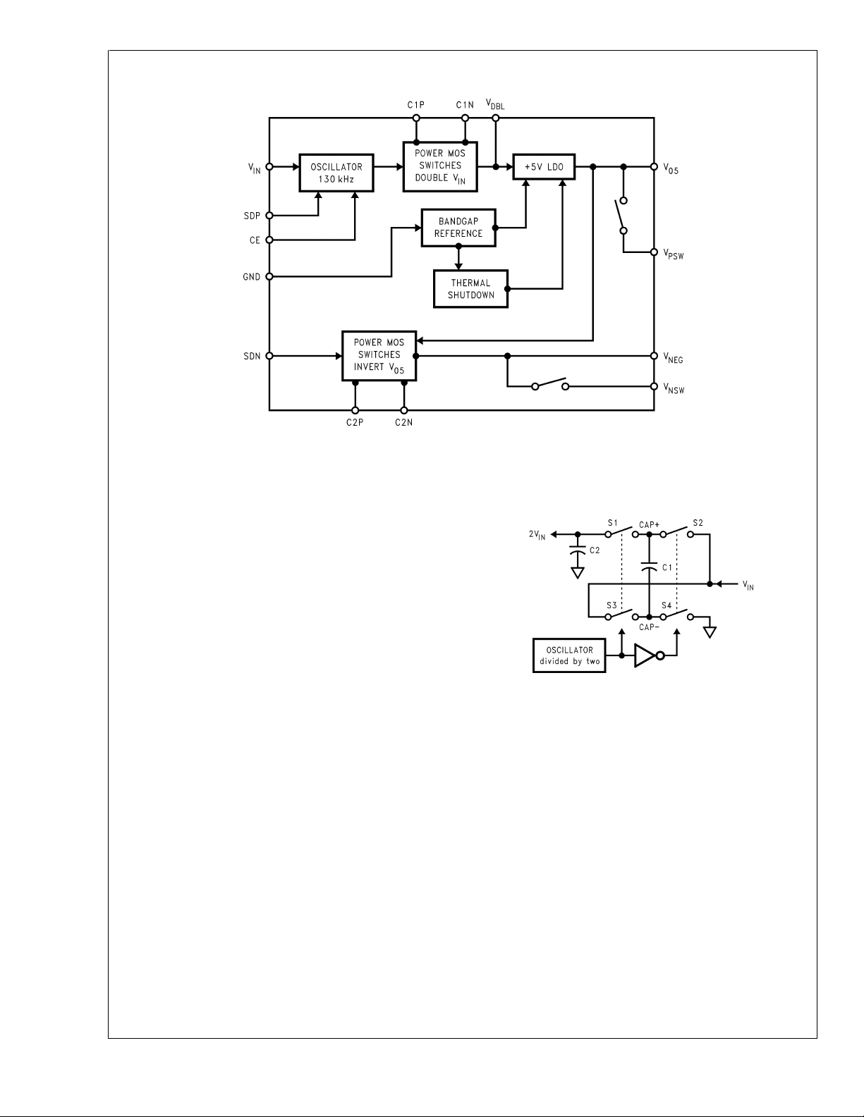
FIGURE 1. Functional Block Diagram
The LM2685 CMOS charge pump voltage converter operates as an input voltage doubler, +5V regulator and inverter
for an input voltage in the range of +2.85V to +6.5V. It delivers maximum load currents of 50mA and 15mA for the regulated +5V and the inverted output voltages respectively, with
an operating current of only 800µA. It also has a typical shutdown current of 6µA. All these performance qualities make
the LM2685 an ideal device for battery powered systems.
The LM2685 has three main functional blocks: a voltage
doubler, a low dropout (LDO) regulator, and a voltage inverter.
Figure 1
shows the LM2685 functional block diagram.
DS101100-3
used for most applications. If the input ramp is less than
10V/ms, a smaller schottky diode like MBR0520LT1 can be
used to reduce the circuit size.
Voltage Doubler
The voltage doubler stage doubles the input voltage V
within the range of +2.85V to +5.4V.For V
above 5.4V, the
IN
IN
doubler shuts off and the input voltage is passed directly to
V
via an internal power switch.
DBL
The doubler contains four large CMOS switches which are
switched in a sequence to double the input supply voltage.
Figure 2
and S4 are closed, C1 charges to the supply voltage V
illustrates the voltage conversion scheme. When S2
IN
During this time interval, switches S1 and S3 are open. Inthe
next time interval, S2 and S4 are opened at the same time,
S1 and S3 are closed, the sum of the input voltage V
the voltage across C1 gives the 2V
C2 gives the 2V
at V
IN
DBL
output. V
regulator. It is recommended not to load V
and the voltage across
In
supplies the LDO
DBL
when V05has
DBL
a load of 50mA. For proper operation, the sum of V
V
loads must not be more than 50mA.
05
DBL
and
IN
and
The Schottky diode D1 is only needed for start-up. The internal oscillator circuit uses the V
and GND pins. The volt-
DBL
age across them must be larger than 1.8V to ensure the operation of the oscillator.During start-up, D1 is used to charge
up the voltage at V
pin to start the oscillator; it also pro-
DBL
tects the device from turning on its own parasitic diode and
potentially latching up. The diode should have enough current carrying capability to change capacitor C3 at start-up, as
well as a low forward voltage to prevent the internal parasitic
diode from turning on. A Schottky diode like 1N5817 can be
,
DS101100-4
FIGURE 2. Voltage Doubler Principle
+5 LDO Regulator
V
is the input to an LDO regulator that regulates it to a +5
DBL
.
switch PSW. The LDO output capacitor (4.7µF Tantalum)
output voltage at V
05.VPSW
may be tied to either V
is tied to V05through a series
or V
05
PSW
.
Inverter
From the V
output, a −5V output is created at V
05
NEG
by
means of an inverting charge pump. This negative output is
unregulated, meaning that it’s output will droop as the load
current at V
increases. The inverter contains four large
NEG
CMOS switches which are in a sequence to invert the input
supply voltage.
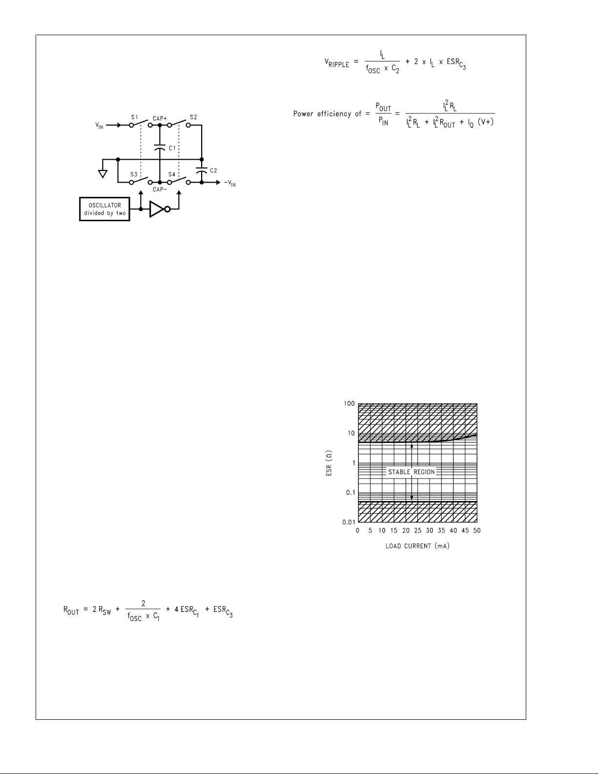
Figure 3
illustrates the voltage conversion
scheme. When S1 and S3 are closed, C1 charges to the
supply voltage V
. During this time interval, switches S2
05
and S4 are open. In the second time interval, S1 and S3 are
open;at the same time, S2 and S4 are closed, C1 is charging
C2. After a number of cycles, the voltage cross C2 will be
pumped to V
ground, the output at the cathode of C2 equals −(V
. Since the anode of C2 is connected to
05
) when
05
there is no load current. The output voltage drop when a load
www.national.com 6
Page 7
Detailed Device Description
(Continued)
LM2685
is added is determined by the parasitic resistance (R
(on) of
ds
the MOSFET switches and the ESR of the capacitors) and
the charge transfer loss between capacitors.
DS101100-5
FIGURE 3. Voltage Inverter Principle
Shutdown and Load Disconnect
In addition to the nominal charge pump and regulator functions, the LM2685 features shutdown and load disconnect
circuitry.CE (chip enable) and SDP (shutdown positive) perform the same task with opposite input polarities. When CE
is low or SDP is high, all circuit blocks are disabled and V
falls to ground potential. This is the same result as when the
die temperature exceeds 150˚C (typical), and the device’s
internal thermal shutdown is triggered.
Forcing SDN (shutdown negative) high disables only the inverting charge pump. The doubling charge pump and the
LDO regulator continue to operate, so the V
and the V
05
PSW
remain at 5V.
The LM2685 incorporates two low impedance switches tied
to the V
05
and V
outputs, because some special applica-
NEG
tions require load disconnect and this is achievable via the
switches. Switch PSW connects V
NSW connects V
NEG
to V
NSW
to V
05
, and switch
PSW
. In normal operation, these
switches are closed, allowing 5V loads to be tied to either
V
or V
05
V
. Driving SDN high opens switch NSW only,while forc-
NSW
and −5V loads to be tied to either V
PSW
NEG
ing CE low or SDP high, opens both the PSW and NSW.
High capacitance (2.2µF to higher), low ESR capacitors can
reduce the output resistance and the voltage ripple.
where IQ(V+) is the quiescent power loss of the IC device,
2
and I
R is the conversion loss associated with the switch
L
on-resistance, the two external capacitors and their ESRs.
Low ESR capacitors (table to be referenced) are recom-
mended to maximize efficiency, reduce the output voltage
drop and voltage ripple.
+5 LDO Regulator External Capacitors
The voltage doubler output capacitor,C3, serves as the input
capacitor of the +5 LDO regulator. The output capacitor C4,
must meet the requirement for minimum amount of capacitance and appropriate ESR (Equivalent Serving Resistance)
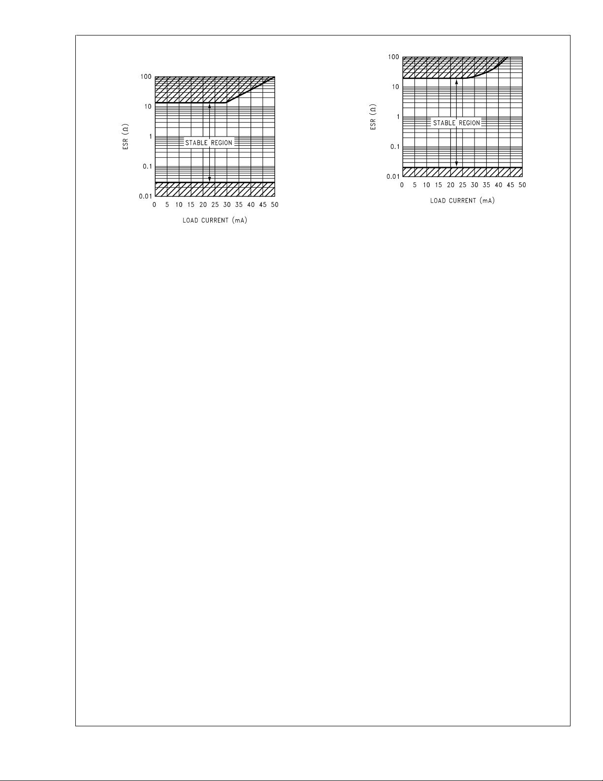
for proper operation. The ESR value must remain within the
regions of stability as shown in
6
to ensure output’s stability.A minimum capacitance of 1µF
Figure 4,Figure 5
and
Figure
is required at the output. This can be increased without limit,
05
but a 4.7µF tantalum capacitor is recommended for loads
ranging upto the maximum specification. With lighter loads
of less or equal to 10mA, ceramic capacitor of at least 1µF
and ESR in the milliohms can be used. This has to be connected to V
pin instead of the V05pin.
PSW
Any output capacitor used should have a good tolerance
over temperature for capacitance and ESR values. The
larger the capacitor, with ESR within the stable region, the
better the stability and noise performance.
or
Application Information
Capacitor Selection
The output resistance and ripple voltage are dependent on
the capacitance and ESR values of the external capacitors.
Voltage Doubler External Capacitors
The selection of capacitors are based on the specifications
of the dropout voltage (which equals I
OUTROUT
voltage ripple, and the converter efficiency.
where RSWis the sum of the ON resistance of the internal
MOSFET switches as shown in
Figure 2
The peak-to-peak output voltage ripple is determined by the
oscillator frequency, the capacitance and ESR of the capacitor C3.
), the output
.
FIGURE 4. ESR Curve for C
OUT
DS101100-25
= 2.2µF
www.national.com7
Page 8
Application Information (Continued)
LM2685
DS101100-27
FIGURE 6. ESR Curve for C
FIGURE 5. ESR Curve for C
OUT
DS101100-26
= 4.7µF
Inverter External Capacitors
As discussed in the +5 LDO Regulator External Capacitors section, the output resistance and ripple voltage are dependent on the
capacitance and ESR values of the external capacitors.Aminimum of 1µF capacitor with good tolerance over temperature for capacitance and ESR values. The capacitance value can be increased without limit while still maintain high low ESR value. 2.2µF
capacitors are recommended for the two external capacitors, C
and C5of the inverter.
2
OUT
=10µF
www.national.com 8
Page 9
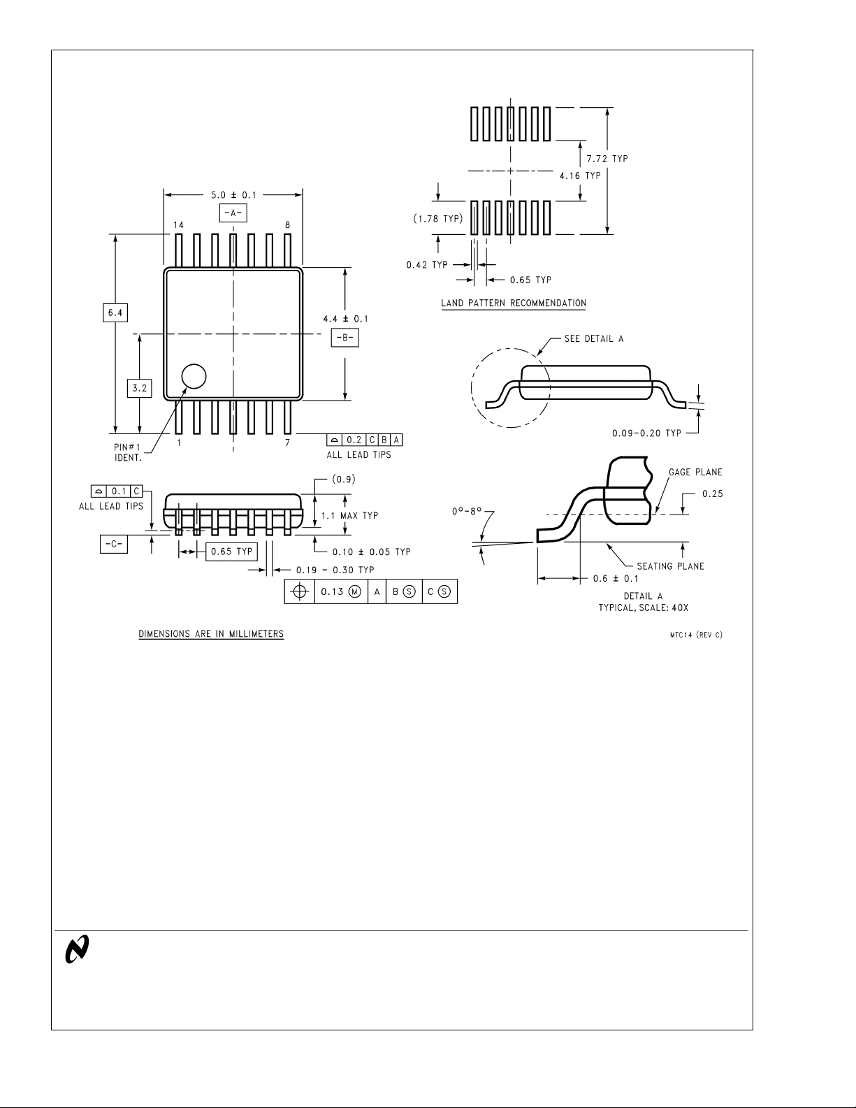
Physical Dimensions inches (millimeters) unless otherwise noted
LM2685 Dual Output Regulated Switched Capacitor Voltage Converter
TSSOP-14 Package
14-Lead Thin Shrink Small-Outline Package
For Ordering, Refer to Ordering Information Table
NS Package Number MTC14
LIFE SUPPORT POLICY
NATIONAL’S PRODUCTS ARE NOT AUTHORIZED FOR USE AS CRITICAL COMPONENTS IN LIFE SUPPORT
DEVICES OR SYSTEMS WITHOUT THE EXPRESS WRITTEN APPROVAL OF THE PRESIDENT AND GENERAL
COUNSEL OF NATIONAL SEMICONDUCTOR CORPORATION. As used herein:
1. Life support devices or systems are devices or
systems which, (a) are intended for surgical implant
into the body, or (b) support or sustain life, and
whose failure to perform when properly used in
accordance with instructions for use provided in the
2. A critical component is any component of a life
support device or system whose failure to perform
can be reasonably expected to cause the failure of
the life support device or system, or to affect its
safety or effectiveness.
labeling, can be reasonably expected to result in a
significant injury to the user.
National Semiconductor
Corporation
Americas
Tel: 1-800-272-9959
Fax: 1-800-737-7018
Email: [email protected]
www.national.com
National does not assume any responsibility for use of any circuitry described, no circuit patent licenses are implied and National reserves the right at any time without notice to change said circuitry and specifications.
National Semiconductor
Europe
Fax: +49 (0) 180-530 85 86
Email: [email protected]
Deutsch Tel: +49 (0) 69 9508 6208
English Tel: +44 (0) 870 24 0 2171
Français Tel: +33 (0) 1 41 91 8790
National Semiconductor
Asia Pacific Customer
Response Group
Tel: 65-2544466
Fax: 65-2504466
Email: [email protected]
National Semiconductor
Japan Ltd.
Tel: 81-3-5639-7560
Fax: 81-3-5639-7507
 Loading...