

Page 1
April 2005
LM2655
2.5A High Efficiency Synchronous Switching Regulator
LM2655 2.5A High Efficiency Synchronous Switching Regulator
General Description
The LM2655 is a current-mode controlled PWM step-down
switching regulator. It has the unique ability to operate in
synchronous or asynchronous mode. This gives the designer flexibility to choose between the high efficiency of
synchronous operation, or the low solution cost of asynchronous operation. Along with flexibility, the LM2655 offers high
power density with the small footprint of a TSSOP-16 package.
>
High efficiency (
internal low ON-resistance (33mΩ) MOSFET, and an external N-Channel MOSFET. This feature, together with its low
quiescent current, makes the LM2655 an ideal fit in portable
applications.
Integrated in the LM2655 are all the power, control, and drive
functions for asynchronous operation. In addition, a low-side
driver output allows easy synchronous operation. The IC
uses patented current sensing circuitry that eliminates the
external current sensing resistor required by other currentmode DC-DC converters. A programmable soft-start feature
limits start up current surges and provides a means of sequencing multiple power supplies.
90%) is obtained through the use of an
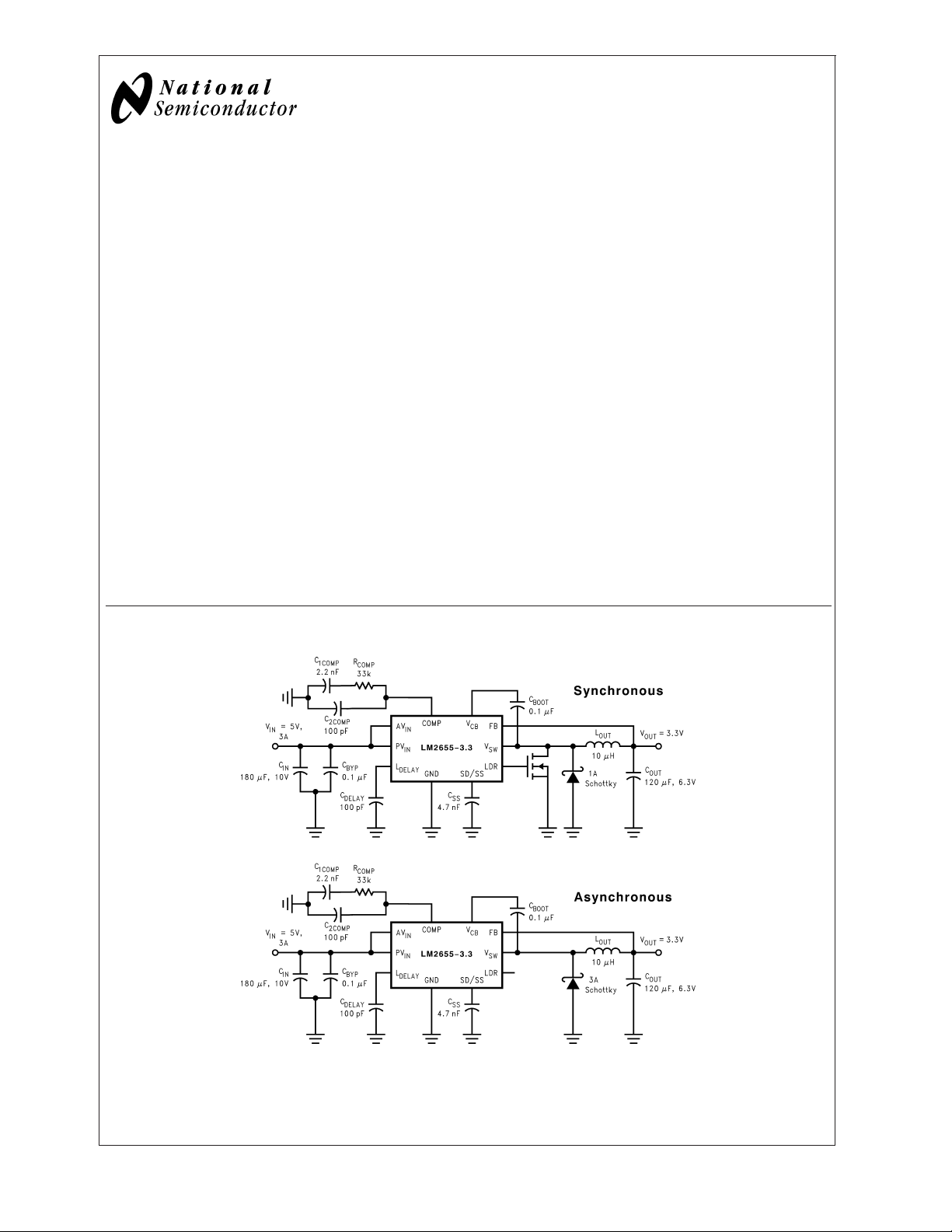
Typical Application
Features
n Ultra-high efficiency up to 96%
n 4V to 14V input voltage range
n Internal high-side MOSFET with low R
n 300 kHz fixed frequency internal oscillator
n Low-side drive for synchronous operation
n Guaranteed less than 12 µA shutdown current
n Patented current sensing for current mode control
n Programmable soft-start
n Input undervoltage lockout
n Output overvoltage shutdown protection
n Output undervoltage shutdown protection
n Thermal Shutdown
n 16-pin TSSOP package
DS(ON)
= 0.033Ω
Applications
n Hard disk drives
n Internet appliances
n TFT monitors
n Computer peripherals
n Battery powered devices
10128429
© 2005 National Semiconductor Corporation DS101284 www.national.com
Page 2
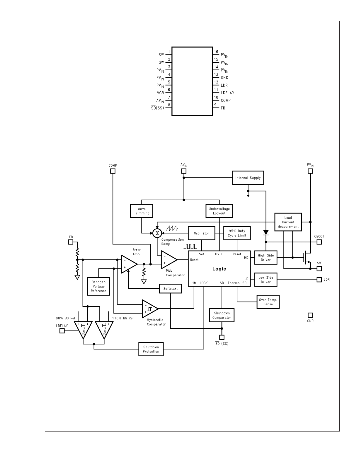
Connection Diagram
LM2655
16-Lead TSSOP (MTC)
Block Diagram
Top View
10128403
Order Number LM2655MTC-ADJ
See NS Package Number MTC16
www.national.com 2
10128404
Page 3

Pin Description
Pin Name Function
1-2 SW Switched-node connection, which is connected to the source of the internal high-side
MOSFET.
3-5 PV
6V
7AV
IN
CB
IN
8 SD(SS)
Main power supply input pin. Connected to the drain of the internal high-side MOSFET.
Bootstrap capacitor connection for high-side gate drive.
Input voltage for control and drive circuits.
Shutdown and Soft-start control pin. Pulling this pin below 0.3V shuts off the regulator. A
capacitor connected from this pin to ground provides a control ramp of the input current.
Do not drive this pin with an external source or erroneous operation may result.
9 FB Output voltage feedback input. Connected to the output voltage.
10 COMP Compensation network connection. Connected to the output of the voltage error amplifier.
11 L
DELAY
A capacitor between this pin to ground sets the delay from when the output voltage
reaches 80% of its nominal to when the undervoltage latch protection is enabled.
12 LDR Low-side FET gate drive pin.
13 GND Power ground.
14-16 PV
IN
Main power supply input pin. Connected to the drain of the internal high-side MOSFET.
Ordering Information
LM2655
Supplied as 1000 units
Tape and Reel
Supplied as 3000 units,
Tape and Reel
LM2655MTC-3.3 LM2655MTCX-3.3
LM2655MTC-ADJ LM2655MTCX-ADJ
www.national.com3
Page 4
Absolute Maximum Ratings (Note 1)
If Military/Aerospace specified devices are required,
LM2655
please contact the National Semiconductor Sales Office/
Distributors for availability and specifications.
Supply Voltage (PV
Supply Voltage (AV
Feedback Pin Voltage -0.4V ≤ V
V
Voltage, (Note 7) 7V
CB
C
Voltage 2.5V
SS
Comp Voltage 2.5V
L
Voltage 2.5V
DELAY
LDR Voltage 5V
V
, (Note 8) 14V
SW
Power Dissipation (T
) 3.8V ≤ VIN≤ 14V
IN
) 4.0V ≤ VIN≤ 14V
IN
=25˚C),
A
≤ 5V
FB
TSSOP-16 Package θ
JA
Power Dissapation 893mW
Lead Temperature
Vapor Phase (60 sec.) 215˚C
Infrared (15 sec.) 220˚C
ESD Susceptibility(Note 3)
Human Body Model(Note 4) 1kV
Machine Model 200V
Operating Ratings (Note 1)
Storage Temperature Range −65˚C ≤ T
Junction Temperature Range −40˚C ≤ T
(Note 2)
LM2655-3.3 Electrical Characteristics
Specifications with standard typeface are for TJ= 25˚C, and those in boldface type apply over full Operating Temperature
Range.V
Symbol Parameter Conditions
V
OUT
V
OUT
V
INUV
V
UV_HYST
ICL(Note 9) Average Output Current
= 10V unless otherwise specified.
IN
Output Voltage I
Output Voltage Line
Regulation
Output Voltage Load
Regulation
VINUndervoltage Lockout
Threshold Voltage
Hysteresis for the Input
Undervoltage Lockout
Limit
Typical
(Note 5)
= 1.5 A 3.3
LOAD
VIN=5Vto14V
= 1.5 A
I
LOAD
I
= 100 mA to 2.5A
LOAD
=10V
V
IN
0.5
0.6
Rising Edge 3.8
210 mV
VIN=5V
= 3.3V
V
OUT
3.3
Limit
(Note 6)
3.235/3.185
3.392/3.416
0.7
1.7
3.95
140˚C/W
≤ +150˚C
J
≤ +125˚C
J
Units
V
V(min)
V(max)
%
%(max)
%
%(max)
V
V(max)
LM2655-ADJ Electrical Characteristics
Specifications with standard typeface are for TJ= 25˚C, and those in boldface type apply over full Operating Temperature
Range.V
Symbol Parameter Conditions
V
FB
V
OUT
V
INUV
V
UV_HYST
(Note 9) Average Output Current
I
CL
www.national.com 4
= 10V unless otherwise specified.
IN
Feedback Voltage I
Output Voltage Line
Regulation
Output Voltage Load
Regulation
VINUndervoltage Lockout
Threshold Voltage
Hysteresis for the Input
Undervoltage Lockout
Limit
Typical
(Note 5)
= 1.5 A 1.238
LOAD
VIN=5Vto14V
= 1.5 A
I
LOAD
I
= 100 mA to 2.5A
LOAD
=10V
V
IN
0.5
0.6
Rising Edge 3.8
210 mV
VIN=5V
= 3.3V
V
OUT
3.3 A
Limit
(Note 6)
1.208/1.181
1.260/1.267
0.7
1.7
3.95
Units
V
V(min)
V(max)
%
%(max)
%
%(max)
V
V(max)
Page 5

All Output Voltage Versions Electrical Characteristics
Specifications with standard typeface are for TJ= 25˚C, and those in boldface type apply over full Operating Temperature
Range.V
Symbol Parameter Conditions
I
Q
I
QSD
R
DS(ON)
R
SW(ON)
I
L
V
BOOT
G
M
A
V
I
EA_SOURCE
I
EA_SINK
V
EAH
V
EAL
F
OSC
D
MAX
I
SS
V
OUTUV
V
OUTOV
I
LDELAY__
SOURCE
I
SHUTDOWN
V
SHUTDOWN
T
SD
= 10V unless otherwise specified.
IN
Quiescent Current Shutdown Pin Floating (Device
Typical
(Note 6)
1.7
Limit
(Note 5)
On)
Quiescent Current in
Shutdown Mode
Switch ON Resistance I
Device Not Switching
Shutdown Pin Pulled Low 7
= 1.5A 33
SWITCH
3
12/20
80
Switch On Resistance
I
= 1.5A 72 mΩ
SWITCH
(MOSFET ON Resistance +
Bonding Wire Resistance)
Switch Leakage Current 5 nA
Bootstrap Regulator Voltage I
BOOT
C
BOOT
=1mA
=tbd
6.7
6.4
7.0
Error Amplifier
1250 µmho
Transconductance
Error Amplifier Voltage Gain 100
Error Amplifier Source
Current
VIN= 4V, VFB= .9*V
=2V
OUT,VCOMP
Error Amplifier Sink Current VIN= 4V, VFB= 1.1*V
=2V
Error Amplifier Output Swing
Upper Limit
Error Amplifier Output Swing
Lower Limit
VIN= 4V, VFB= .9*V
=2V
VIN= 4V, VFB= .9*V
=2V
OUT,VCOMP
OUT,VCOMP
Oscillator Frequency Measured at Switch Pin
=4V
V
IN
OUT,VCOMP
40
32/10
80
53/30
2.70
2.50/2.40
1.25
1.35/1.50
300
280/255
330/345
Maximum Duty Cycle VIN=4V 95
92
Soft-Start Current Voltage at the SS Pin = 1.4V 11
14
V
Undervoltage Lockout
OUT
Threshold Voltage
81
76
84
Hysteresis for V
V
Overvoltage Lockout
OUT
OUTUV
Threshold Voltage
5%V
108
106
114
Hysteresis for V
OUTOV
5%V
LDELAY Pin Source Current 5 µA
Shutdown Pin Current Shutdown Pin Pulled Low 2.2
3.7/4.0
Shutdown Pin Threshold
Voltage
Rising Edge 0.6
0.25
0.9
Thermal Shutdown
165 ˚C
Temperature
Units
mA(max)
µA(max)
mΩ(max)
V(min)
V(max)
µA(min)
µA(min)
V(min)
V(max)
kHz
kHz(min)
kHz(max)
%(min)
µA(max)
%V
%V
OUT
%V
OUT
%V
%V
OUT
%V
OUT
µA(max)
V(min)
V(max)
LM2655
mA
µA
mΩ
V
µA
µA
V
V
%
µA
OUT
(min)
(max)
OUT
OUT
(min)
(max)
OUT
µA
V
www.national.com5
Page 6

All Output Voltage Versions Electrical Characteristics (Continued)
Specifications with standard typeface are for TJ= 25˚C, and those in boldface type apply over full Operating Temperature
LM2655
Range.V
Symbol Parameter Conditions
T
SD_HYST
= 10V unless otherwise specified.
IN
Thermal Shutdown
Typical
(Note 6)
Limit
(Note 5)
25 ˚C
Hysteresis Temperature
Low-side Driver (LDR) Parameters
Specifications with standard typeface are for TJ= 25˚C, and those in boldface type apply over full Operating Temperature
Range.V
Symbol Parameter Conditions
V
OH
V
OL
I
SINK
I
SOURCE
T
RR
T
F
Note 1: Absolute Maximum Ratings indicate limits beyond which damage to the device may occur. Operating Ratings indicate conditions for which the device is
intended to be functional, but device parameter specifications may not be guaranteed under these conditions. For guaranteed specifications and test conditions, see
the Electrical Characteristics.
Note 2: The maximum allowable power dissipation is calculated by using P
ambient temperature, and θ
140˚C/W for T
allows the safe dissipation of more power. The Absolute Maximum power dissipation must be derated by 7.14 mW per ˚C above 25˚C ambient. The LM2655 actively
limits its junction temperatures to about 165˚C.
Note 3: The human body model is a 100 pF capacitor discharged through a 1.5 kΩ resistor into each pin. The machine model is a 200pF capacitor discharged
directly into each pin.
Note 4: ESD susceptibility using the human body model is 500V for V
Note 5: Typical numbers are at 25˚C and represent the most likely norm.
Note 6: All limits guaranteed at room temperature (standard typeface) and at temperature extremes (bold typeface). All room temperature limits are 100%
production tested. All limits at temperature extremes are guaranteed via correlation using standard Statistical Quality Control (SQC) methods. All limits are used
to calculate Average Outgoing Quality Level (AOQL).
Note 7: Measured with respect to V
Note 8: Measured while switching in closed loop with Vin = 15V.
Note 9: Average output current limit obtained using typical application circuit. This figure is dependant on the the inductor used.
Note 10: Bond wire resistance accounts for approximately 40mΩ of R
= 10V unless otherwise specified.
IN
Typical
(Note 5)
Limit
(Note 6)
Logic High Level VIN= 10V 6.8
6.6
= 6.0V 6
V
IN
5.8
Logic Low Level 0
0.05
LDR Sink Current LDR Voltage = 1V 500 mA
LDR Source Current LDR Voltage = 2V 180 mA
Rise Time CGS=1000pF 18 ns
Fall Time CGS=1000pF 7 ns
=(T
is the junction-to-ambient thermal resistance of the specified package. The 893 mW rating results from using 150˚C, 25˚C, and
JA
, and θJArespectively. A θJAof 140˚C/W represents the worst-case condition of no heat sinking of the 16-pin TSSOP package. Heat sinking
JMAX,TA
.
SW
DMAX
CB,VSW
SW(ON)
, LDR, and L
.
JMAX−TA
DELAY
)/θJA, where T
.
is the maximum junction temperature, TAis the
JMAX
Units
Units
V
V(min)
V
V(min)
V
V(max)
www.national.com 6
Page 7

Typical Performance Characteristics
LM2655
Efficiency vs Load Current
(V
= 5V, V
IN
lQvs V
OUT
= 3.3V)
IN
10128405
Efficiency vs V
(I
= 0.5A) (Synchronous)
LOAD
I
QSD
vs V
IN
10128406
IN
10128407 10128408
I
vs Junction Temperature Frequency vs Junction Temperature
QSD
10128409 10128410
www.national.com7
Page 8

Typical Performance Characteristics (Continued)
LM2655
R
Input Voltage (Note 10) (I
+ Bond Wire Resistance vs
SW(ON)
LOAD
Current Limit vs Input Voltage
(Synchronous)
= 1.5A)
10128411
R
+ Bond Wire Resistance vs
SW(ON)
Junction Temperature (Note 10) (I
Current Limit vs Input Voltage
(Asynchronous)
= 1.5A, VIN=5V)
LOAD
10128412
10128413
Current Limit vs Junction Temperature
(V
= 5V, V
IN
= 3.3V) Reference Voltage vs Junction Temperature
OUT
10128415
10128414
10128416
www.national.com 8
Page 9

Operation
The LM2655 is a constant frequency (300kHz), currentmode PWM switcher that can be operated synchronously or
asynchronously.
SYNCHRONOUS OPERATION
A converter is said to be in synchronous operation when a
MOSFET is used in place of the catch diode. In the case of
the buck converter, this MOSFET is known as the low-side
MOSFET (the MOSFET connected between the input
source and the low-side MOSFET is the high-side MOSFET). Converters in synchronous operation exhibit higher
efficiencies compared to asynchronous operation because
2
R losses are reduced with the use of a MOSFET .
the I
Operation of the LM2655 in synchronous mode is identical to
its operation in asynchronous mode, except that internal
logic drives the low-side MOSFET. At the beginning of a
switching cycle, the high-side MOSFET is on and current
from the input source flows through the inductor and to the
load. The current from the high-side MOSFET is sensed and
compared with the output of the error amplifier (COMP pin).
When the sensed current reaches the COMP pin voltage
level, the high-side switch is turned off. After a 30ns delay
(deadtime), the low-side driver goes high and turns the
low-side MOSFET on. The current now flows through the
low-side MOSFET, through the inductor and on to the load. A
30ns delay is necessary to insure that the MOSFETs are
never on at the same time. During the 30ns deadtime, the
current is forced to flow through the low-side MOSFET’s
body diode. It is recommended that a low forward drop
schottky diode be placed in parallel to the low-side MOSFET
so that current will be more efficiently conducted during this
30ns deadtime. This Schottky diode should be placed within
5mm of the switch pin so that current limit is not effected (see
External Schottky Diode section). At the end of the switching
cycle, the low-side switch is turned off and after another
30ns delay, the cycle is repeated.
Current through the high-side MOSFET is sensed by patented circuitry that does not require an external sense resistor. As a result, system cost and size are reduced, efficiency
is increased, and noise immunity of the sensed current is
improved. A feedforward from the input voltage is added to
reduce the variation of the current limit over the input voltage
range.
ASYNCHRONOUS OPERATION
A unique feature of the LM2655 is that it can be operated in
either synchronous or asynchronous mode. When operating
in asynchronous mode, a small amount of efficiency is sacrificed for a less expensive solution. Any diode may be used,
but it is recommended that a low forward drop schottky diode
be use to maximize efficiency. When operating the LM2655
in asynchronous mode, the LDR pin should be terminated
with a large resistor (
asynchronous mode is similar to that of synchronous mode,
except the internal low-side MOSFET logic is not used. At
the beginning of a switching cycle, the high-side MOSFET is
on and current from the input source flows through the
inductor and to the load. The current from the high-side
MOSFET is sensed and compared with the output of the
error amplifier (COMP pin). When the sensed current
reaches the COMP pin voltage level, the high-side switch is
turned off. At this instant, the load current is commutated
through the catch diode. The current now flows through the
diode and the inductor and on to the load. At the end of the
switching cycle, the high-side switch is turned on and the
cycle is repeated.
PROTECTIONS
The peak current in the system is monitored by cycle-bycycle current limit circuitry. This circuitry will turn the highside MOSFET off whenever the current through the highside MOSFET reaches a preset limit (see plots). A second
level current limit is accomplished by the undervoltage protection: if the load pulls the output voltage down below 80%
of its nominal value, the undervoltage latch protection will
wait for a period of time (set by the capacitor at the LDELAY
pin, see LDELAY CAPACITOR section for more information).
If the output voltage is still below 80% of its nominal after the
waiting period, the latch protection will be enabled. In the
latch protection mode, the low-side MOSFET is on and the
high-side MOSFET is off. The latch protection will also be
enabled immediately whenever the output voltage exceeds
the overvoltage threshold (110% of its nominal). Both protections are disabled during start-up.(See SOFT-START CAPACITOR section and LDELAY CAPACITOR section for
more information.) Toggling the input supply voltage or the
shutdown pin can reset the device from the latched protection mode.
>
1 MegΩ), or left floating. Operation in
LM2655
Design Procedure
This section presents guidelines for selecting external components.
INPUT CAPACITOR
A low ESR aluminum, tantalum, ceramic, or any other type of
capacitor is needed between the input pin and power
ground. This capacitor prevents large voltage transients from
appearing at the input. The capacitor is selected based on
the RMS current and voltage requirements. The RMS current is given by:
The RMS current reaches its maximum (I
equals 2V
V
IN
the voltage rating should be at least 25% higher than the
maximum input voltage. If a tantalum capacitor is used, the
voltage rating required is about twice the maximum input
. For an aluminum or ceramic capacitor,
OUT
OUT
/2) when
voltage. The tantalum capacitor should be surge current
tested by the manufacturer to prevent damage by the inrush
current. It is also recommended to put a small ceramic
capacitor (0.1 µF) between the input pin and ground pin to
reduce high frequency noise.
INDUCTOR
The most critical parameters for the inductor are the inductance, peak current and the DC resistance. The inductance
is related to the peak-to-peak inductor ripple current, the
input and the output voltages:
A higher value of ripple current reduces inductance, but
increases the conductance loss, core loss, current stress for
the inductor and switch devices. It also requires a bigger
output capacitor for the same output voltage ripple require-
www.national.com9
Page 10

Design Procedure (Continued)
ment. A reasonable value is setting the ripple current to be
LM2655
30% of the DC output current. Since the ripple current increases with the input voltage, the maximum input voltage is
always used to determine the inductance. The DC resistance
of the inductor is a key parameter for the efficiency. Lower
DC resistance is available with a bigger winding area. A good
tradeoff between the efficiency and the core size is letting the
inductor copper loss equal 2% of the output power.
OUTPUT CAPACITOR
The selection of C
mum allowable output voltage ripple. The output ripple in the
constant frequency, PWM mode is approximated by:
The ESR term usually plays the dominant role in determining
the voltage ripple. A low ESR aluminum electrolytic or tantalum capacitor (such as Nichicon PL series, Sanyo OS-CON,
is primarily determined by the maxi-
OUT
Sprague 593D, 594D, AVX TPS, and CDE polymer aluminum) is recommended. An electrolytic capacitor is not recommended for temperatures below −25˚C since its ESR
rises dramatically at cold temperature. A tantalum capacitor
has a much better ESR specification at cold temperature and
is preferred for low temperature applications.
The output voltage ripple in constant frequency mode has to
be less than the sleep mode voltage hysteresis to avoid
entering the sleep mode at full load:
<
V
RIPPLE
20mV * V
OUT/VFB
10128421
FIGURE 1. Low-side/high-side driver timing diagram.
TABLE 1. MOSFET Manufacturers
Manufacturer Model Number Package Type www Address Phone Fax
Fairchild
FDC653N SuperSOT-6 www.fairchildsemi.com 888-522-5372 207-761-6020
Semiconductor
General
GF4420 SO-8 www.gensemi.com 631-847-3000 631-847-3236
Semiconductor
International
IRF7807 SO-8 www.irf.com 310-322-3331 310-322-3332
Rectifier
Vishay Siliconix Si4812DY SO-8 www.vishay.com 800-554-5565 408-567-8995
Si4874DY SO-8
Zetex ZXM64N03X SO-8 www.zetex.com (44) 161-622-4422 (44) 161-622-4420
LOW-SIDE MOSFET SELECTION
When operating in synchronous mode, special attention
should be given to the selection of the low-side MOSFET.
Besides choosing a MOSFET with minimal size and on
resistance, it is critical that the MOSFET meet certain rise
and fall time specifications. A 30ns deadtime between the
low-side and high-side MOSFET switching transitions is programmed into the LM2655, as shown in Figure 1. The prevent shoot-through current, the low-side MOSFET must turn
off before the high-side MOSFET turns on. Hence, the low-
side MOSFET has 30ns to turn off from the time the low-side
driver goes low. The fall time of the low-side MOSFET is
governed by the equation:
C=CIN
*dVC/dt.
is the LDR sink current capability, CINis the equiva-
C
is limited by the low-side
C
is fixed by the MOSFET.
IN
is the gate-to-
C
I
where I
lent capacitance seen at the LDR pin, and V
source voltage of the MOSFET. I
driver of the LM2655, but C
Therefore, it is important that the chosen MOSFET has a
suitable C
so that the LM2655 will be able to turn it off
IN
www.national.com 10
Page 11

Design Procedure (Continued)
within 30ns. An input capacitance of less than 1000pF is
recommended. Several suitable MOSFETs are shown in
Table 1.
EXTERNAL SCHOTTKY DIODE (Syncronous)
A Schottky diode is recommended to prevent the intrinsic
body diode of the low-side MOSFET from conducting during
the deadtime in PWM operation. If the body diode turns on,
there is extra power dissipation in the body diode because of
the reverse-recovery current and higher forward voltage
drop. In addition, the high-side MOSFET has more switching
loss because the diode reverse-recovery current adds to the
high-side MOSFET turn-on current. These losses degrade
the efficiency by 1-2%. The improved efficiency and noise
immunity with the Schottky diode become more obvious with
increasing input voltage and load current.
It is important to place the diode very close to the switch pin
of the LM2655. Extra parasitic impedance due to the trace
between the switch pin and the cathode of the diode will
cause the current limit to decrease. The breakdown voltage
rating of the diode is preferred to be 25% higher than the
maximum input voltage. Since it is on for a short period of
time, the diode’s average current rating need only be 30% of
the maximum output current.
EXTERNAL SCHOTTKY DIODE (Asyncronous)
In asyncronous mode, the output current commutates
throught the schottky diode when the high-side MOSFET is
turned off. Using a schottky diode with low forward voltage
drop will minimize the effeciency loss in the diode. However,
to achieve the greatest efficiency, the LM2655 should be
operated in syncronous mode using a low-side MOSFET.
Since the Schottky diode conducts for the entire second half
of the duty cycle in asyncronous mode, it should be rated
higher than the full load current.
T
SS=CSS
* 0.6V/2 µA + CSS* (2V−0.6V)/10 µA
During start-up, the internal circuit is monitoring the soft-start
voltage. When the softstart voltage reaches 2V, the undervoltage and overvoltage protections are enabled.
If the output voltage doesn’t rise above 80% of the normal
value before the soft-start reaches 2V, undervoltage protection shut down the device. You can avoid this by either
increasing the value of the soft-start capacitor, or using a
LDELAY capacitor.
LDELAY CAPACITOR
The LDELAY capacitor (CDELAY) provides a means to control undervoltage latch protection. By changing CDELAY, the
user can adjust the time delay between the output voltage
dropping below 80% of its nominal value and the part shutting off due to undervoltage latch protection. The LDELAY
circuit consists ofa5µAcurrent source in series with a user
defined capacitor, CDELAY. The 5 µA current source is
turned on whenever the output voltage is below 80% of its
nominal value, otherwise this current source is off. With the
output voltage below 80% of its nominal value, the 5 µA
current source begins to charge CDELAY, as shown in Fig-
ure 2. If the potential across CDELAY reaches 2V, undervoltage latch protection will be enabled and the part will shutdown. If the output voltage recovers to above 80% of its
nominal value before the potential across CDELAY reaches
2V, undervoltage latch protection will remain disabled.
Hence, CDELAY sets a time delay by the following equation:
T
DELAY
(ms) = C
DELAY
(nF) * 2V/5A
Undervoltage latch protection can be disabled by tying the
LDELAY pin to the ground.
LM2655
BOOST CAPACITOR
The boost capacitor provides the extra votage needed to
turn the high-side, n-channel MOSFET on. A 0.1 µF ceramic
capacitor is recommended for the boost capacitor. The typical voltage across the boost capacitor is 6.7V.
SOFT-START CAPACITOR
A soft-start capacitor is used to provide the soft-start feature.
When the input voltage is first applied, or when the SD(SS)
pin is allowed to go high, the soft-start capacitor is charged
by a current source (approximately 2 µA). When the SD(SS)
pin voltage reaches 0.6V (shutdown threshold), the internal
regulator circuitry starts to operate. The current charging the
soft-start capacitor increases from 2 µA to approximately
10 µA. With the SD(SS) pin voltage between 0.6V and 1.3V,
the level of the current limit is zero, which means the output
voltage is still zero. When the SD(SS) pin voltage increases
beyond 1.3V, the current limit starts to increase. The switch
duty cycle, which is controlled by the level of the current limit,
starts with narrow pulses and gradually gets wider. At the
same time, the output voltage of the converter increases
towards the nominal value, which brings down the output
voltage of the error amplifier. When the output of the error
amplifier is less than the current limit voltage, it takes over
the control of the duty cycle. The converter enters the normal
current-mode PWM operation. The SD(SS) pin voltage is
eventually charged up to about 2V.
The soft-start time can be estimated as:
10128422
FIGURE 2. Undervoltage latch protection.
COMPENSATION COMPONENTS
In the control to output transfer function, the first pole F
be estimated as 1/(2πR
OUTCOUT
output capacitor is 1/(2πESRC
frequency pole F
whereD=V
IN
and V
and V
in the range of 45kHz to 150kHz:
p2
F
p2=Fs
, n = 1+0.348L/(VIN−V
OUT/VIN
in volts).
OUT
The total loop gain G is approximately 1000/I
); The ESR zero Fz1of the
); Also, there is a high
OUT
/(πn(1−D))
)(LisinµHs
OUT
OUT
p1
where I
can
OUT
is in amperes.
A Gm amplifier is used inside the LM2655. The output resis-
of the Gm amplifier is about 80kΩ.Cc1and R
tor R
o
together with Rogive a lag compensation to roll off the gain:
= 1/(2πCc1(Ro+Rc)), F
F
pc1
= 1/2πCc1Rc.
zc1
C
www.national.com11
Page 12

Design Procedure (Continued)
In some applications, the ESR zero F
LM2655
. Then, Cc2is needed to introduce F
by F
p2
ESR zero, F
= 1/(2πCc2Ro\Rc).
p2
The rule of thumb is to have more than 45˚ phase margin at
the crossover frequency (G=1).
is higher than 68µF, Cc1= 2.2nF, and Rc= 15KΩ are
If C
OUT
good choices for most applications. If the ESR zero is too
low to be cancelled by F
, add Cc2.
p2
If the transient response to a step load is important, choose
to be higher than 10kΩ.
R
C
can not be cancelled
z1
pc2
to cancel the
Application Circuits
PROGRAMMABLE OUTPUT VOLTAGE
Using the adjustable output version of the LM2655 as shown
in Figure 3, output voltages between 1.24V and 13V can be
achieved. Use the following formula to select the appropriate
resistor values:
*(V
OUT-VREF
where V
REF
R
FB1=RFB2
= 1.238V.
Select resistors between 10kΩ and 100kΩ. (1% or higher
accuracy metal film resistors for R
FB1
)/V
and R
REF
FB2
.)
10128425
FIGURE 3. Programmable output voltage.
EXTENDING INPUT VOLTAGE RANGE
Figure 4 shows a way to configure the LM2655 so that input
voltages of less than 4V can be converted. This circuit
makes use of the separate analog and power V
pins. All
IN
the supervisory circuits of the LM2655 are powered through
the AV
is input to the PV
has an operating range of 4V
within this range must be applied to AV
pin, while the source voltage that is to be converted
IN
pins. The internal circuitry of the LM2655
IN
<
<
V
14V, so a voltage
CC
. This source may
IN
be low power because it only needs to supply 5mA. An input
capacitor should be connected across this source, and a
small bypass capacitor should be placed physically close to
the AV
pin to ground. With all the internal circuitry being
IN
powered by a separate source, the only requirement of the
voltage at PV
desired output voltage. The source connected to PV
is that it be slightly higher (∼500mV) than the
IN
will
IN
also need an input capacitor and bypass capacitor, but the
input capacitor must be selected following the guidelines
explained in the INPUT CAPACITOR section.
10128423
FIGURE 4. Extended input voltage range.
www.national.com 12
Page 13

Application Circuits (Continued)
OBTAINING OUTPUT VOLTAGES OF LESS THAN 1.25V
Some applications require output voltages less than 1.25V.
The circuit shown in Figure 5 will allow the LM2655 to do
such a conversion. By referencing the two feedback resistors to V
to V
ADJ(VADJ
by the equation:
ADJ
>
1.24V), V
can be adjusted from 0V
OUT
V
=(V
OUT
where V
V
REF
= 1.24V. V
REF
(1.24V). In Figure 5,V
REF-VADJ
)*(R
FB1+RFB2
can be any voltage higher than
ADJ
ADJ
)/R
is produced by an LMV431
adjustable reference following the equation:
V
ADJ
= 1.24*(R
ADJ1/RADJ2
+ 1).
LM2655
FB2+VADJ
10128424
FIGURE 5. Obtaining output voltages of less than 1.25V
Pcb Layout Considerations
Layout is critical to reduce noise and ensure specified performance. The important guidelines are listed as follows:
1. Minimize the parasitic inductance in the loop of input
capacitors and the internal MOSFETs by connecting the
input capacitors to V
wide traces. The high frequency ceramic bypass capacitor, in particular, should be placed as close to and no
more than 5mm from the V
because the rapidly switching current, together with wiring inductance can generate large voltage spikes that
may result in noise problems.
2. Minimize the trace from the center of the output resistor
divider to the FB pin and keep it away from noise
and PGND pins with short and
IN
pin. This is important
IN
sources to avoid noise pick up. For applications that
require tight regulation at the output, a dedicated sense
trace (separated from the power trace) is recommended
to connect the top of the resistor divider to the output.
3. If the Schottky diode D is used, minimize the traces
connecting D to SW and PGND pins. Use short and wide
traces.
4. If the low-side MOSFET is used, minimize the trace
connecting the LDR pin to the gate of the MOSFET, and
the traces to SW and PGND pins. Use short and wide
traces for the power traces going from the MOSFET to
SW and PGND pins.
www.national.com13
Page 14

LM2655
Schematic for the Typical Board Layout
Typical PC Board Layout: (2X Size)
Component Placement Guide
10128425
10128426
Component Side PC Board Layout
www.national.com 14
10128427
Page 15

Typical PC Board Layout: (2X Size) (Continued)
LM2655
Solder Side PC Board Layout
10128428
www.national.com15
Page 16

Physical Dimensions inches (millimeters)
unless otherwise noted
16-Lead TSSOP (MTC)
NS Package Number MTC16
Order Number LM2655MTC-ADJ
LM2655MTCX-ADJ
LM2655MTC-3.3
LM2655MTCX-3.3
See Ordering Information Table For Order Quantities
LM2655 2.5A High Efficiency Synchronous Switching Regulator
National does not assume any responsibility for use of any circuitry described, no circuit patent licenses are implied and National reserves
the right at any time without notice to change said circuitry and specifications.
For the most current product information visit us at www.national.com.
LIFE SUPPORT POLICY
NATIONAL’S PRODUCTS ARE NOT AUTHORIZED FOR USE AS CRITICAL COMPONENTS IN LIFE SUPPORT DEVICES OR SYSTEMS
WITHOUT THE EXPRESS WRITTEN APPROVAL OF THE PRESIDENT AND GENERAL COUNSEL OF NATIONAL SEMICONDUCTOR
CORPORATION. As used herein:
1. Life support devices or systems are devices or systems
which, (a) are intended for surgical implant into the body, or
(b) support or sustain life, and whose failure to perform when
properly used in accordance with instructions for use
2. A critical component is any component of a life support
device or system whose failure to perform can be reasonably
expected to cause the failure of the life support device or
system, or to affect its safety or effectiveness.
provided in the labeling, can be reasonably expected to result
in a significant injury to the user.
BANNED SUBSTANCE COMPLIANCE
National Semiconductor manufactures products and uses packing materials that meet the provisions of the Customer Products
Stewardship Specification (CSP-9-111C2) and the Banned Substances and Materials of Interest Specification (CSP-9-111S2) and contain
no ‘‘Banned Substances’’ as defined in CSP-9-111S2.
National Semiconductor
Americas Customer
Support Center
Email: new.feedback@nsc.com
Tel: 1-800-272-9959
www.national.com
National Semiconductor
Europe Customer Support Center
Fax: +49 (0) 180-530 85 86
Email: europe.support@nsc.com
Deutsch Tel: +49 (0) 69 9508 6208
English Tel: +44 (0) 870 24 0 2171
Français Tel: +33 (0) 1 41 91 8790
National Semiconductor
Asia Pacific Customer
Support Center
Email: ap.support@nsc.com
National Semiconductor
Japan Customer Support Center
Fax: 81-3-5639-7507
Email: jpn.feedback@nsc.com
Tel: 81-3-5639-7560
 Loading...