

Page 1
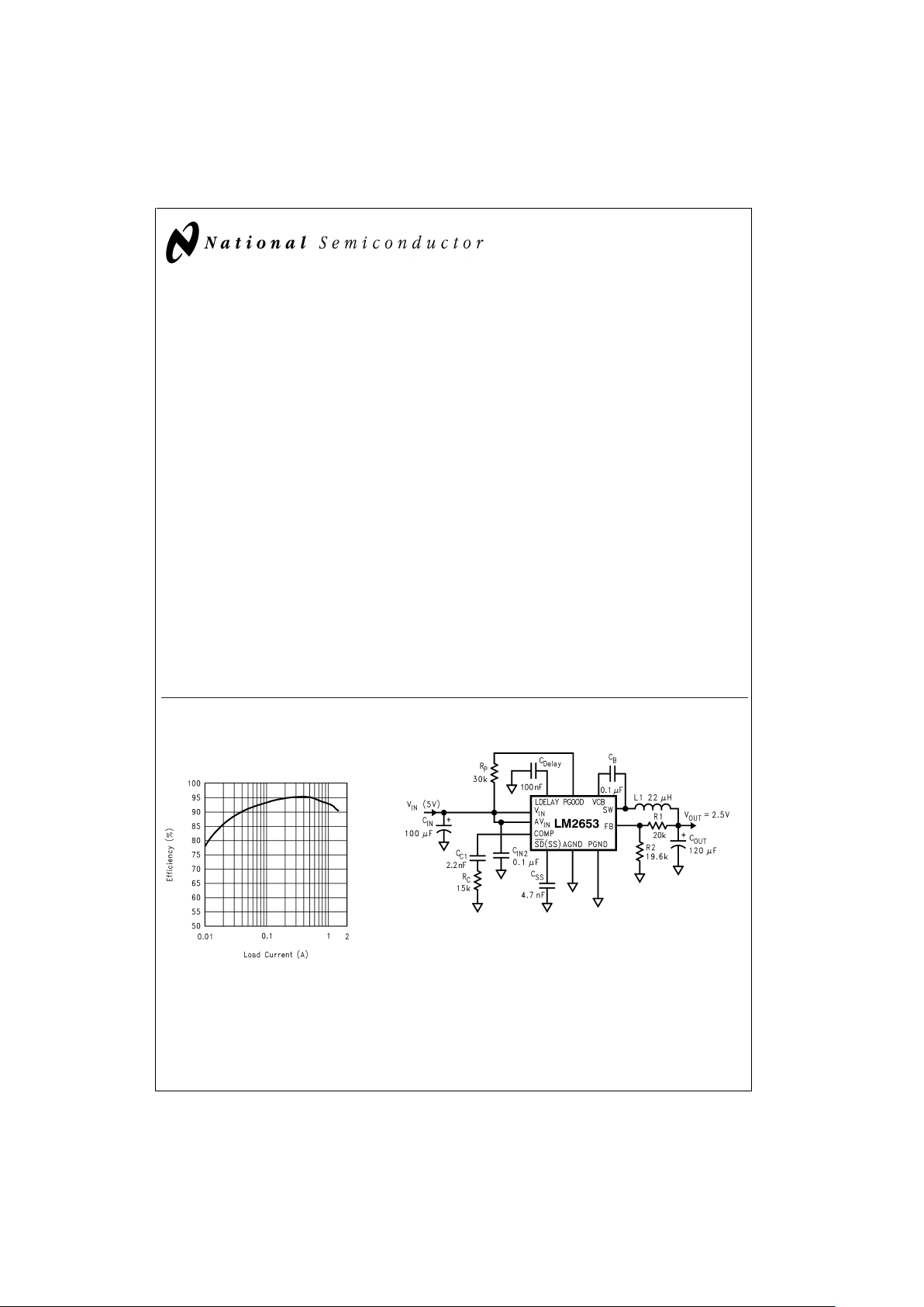
LM2653
1.5A High Efficiency Synchronous Switching Regulator
General Description
The LM2653 switching regulator provides high efficient
power conversion over a 100:1 load range (1.5A to 15 mA).
This feature makes the LM2653 an ideal fit in
battery-powered applications.
Synchronous rectification is used to achieve up to 97%efficiency.At lightloads, the LM2653enters a lowpower hysteretic or “sleep” mode to keep the efficiency high.In many applications, the efficiency still exceeds 80%at 15 mA load. A
shutdown pin is available to disable the LM2653 and reduce
the supply current to 7µA.
All the power, control, and drive functions are integrated
within the ICs.The ICs contain patented current sensing circuity forcurrent mode control. This featureeliminates the external current sensing resistor required by other
current-mode DC-DC converters.
The ICs have a 300 kHz fixed frequency internal oscillator.
The high oscillator frequency allows the use of extremely
small, low profile components.
Protection features include thermal shutdown, input undervoltage lockout, adjustable soft-start, cycle by cycle current
limit, output overvoltage and undervoltage protections.
Features
n Efficiency up to 97
%
n 4V to 14V input voltage range
n 1.5V to 5.0V adjustable output voltage
n 0.1Ω Switch On Resistance
n 300 kHz fixed frequency internal oscillator
n 7 µA shutdown current
n Patented current sensing for current mode control
n Input undervoltage lockout
n Output overvoltage shutdown protection
n Output undervoltage shutdown protection
n Adjustable soft-start
n Adjustable PGOOD delay
n Current limit and thermal shutdown
Applications
n Webpad
n Personal digital assistants (PDAs)
n Computer peripherals
n Battery-powered devices
n Notebook computer video supply
n Handheld scanners
n GXM I/O and core voltage
n High efficiency 5V conversion
Typical Application
Efficiency vs Load Current
(V
IN
=
5V, V
OUT
=
3.3V)
DS101049-2
DS101049-30
November 1999
LM2653 1.5A High Efficiency Synchronous Switching Regulator
© 1999 National Semiconductor Corporation DS101049 www.national.com
Page 2
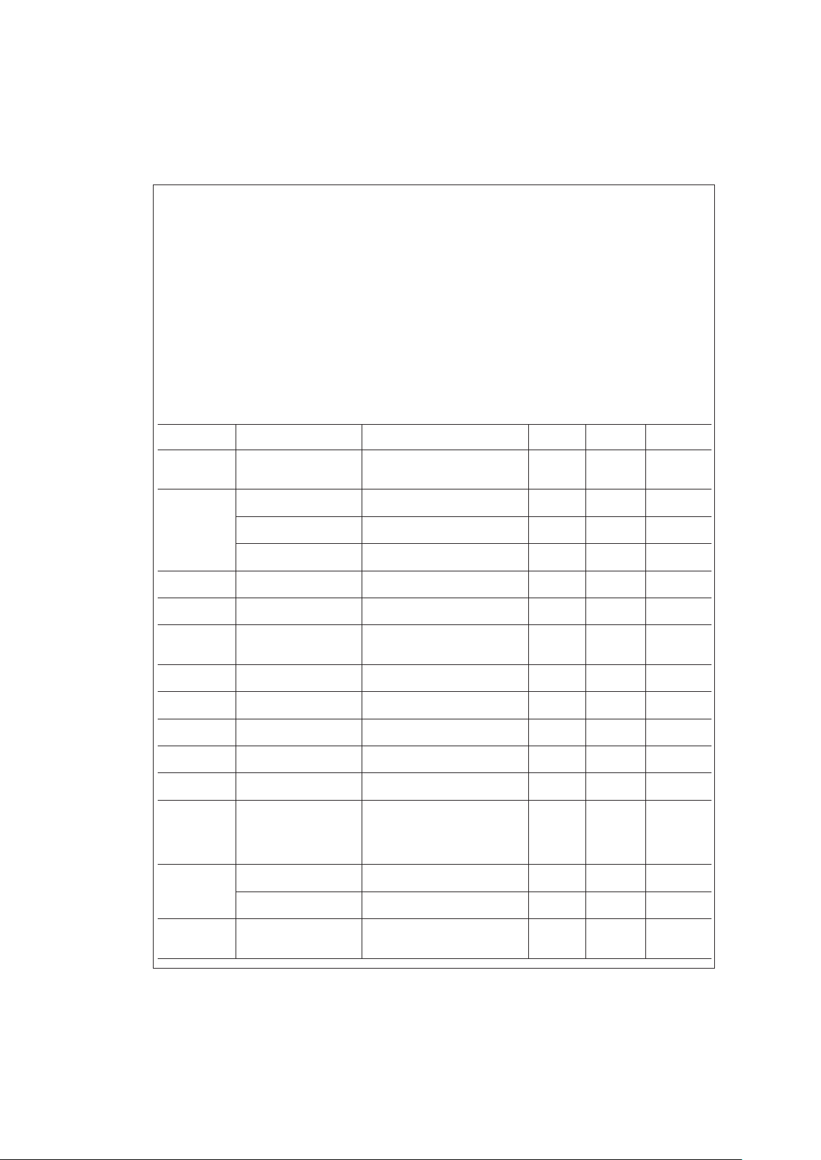
Absolute Maximum Ratings (Note 1)
If Military/Aerospace specified devices are required,
please contactthe National Semiconductor Sales Office/
Distributors for availability and specifications.
Input Voltage 15V
PGOOD Pin Voltage 15V
Feedback Pin Voltage −0.4V ≤ V
FB
≤ 5V
Power Dissipation (T
A
=
25˚C),
(Note 2) 893 mW
Junction Temperature
Range −40˚C ≤ T
J
≤ +125˚C
Storage Temperature Range −65˚C to +150˚C
Lead Temperature
M Package
Vapor Phase (60 sec.) 215˚C
Infrared (15 sec.) 220˚C
Maximum Junction
Temperature
150˚C
ESD Susceptibility
Human Body Model (Note 3) 1 kV
Operating Ratings (Note 1)
Supply Voltage 4V ≤ V
IN
≤ 14V
Electrical Characteristics
Specifications with standard typeface are for T
J
=
25˚C, and those in boldface type apply over full Operating Temperature
Range.V
IN
=
10V unless otherwise specified.
Symbol Parameter Conditions
Typical
(Note 5)
Limit
(Note 4)
Units
V
FB
Feedback Voltage I
LOAD
=
900 mA 1.238
1.200
1.263
V
V(min)
V(max)
V
OUT
Output Voltage Line
Regulation
V
IN
=
4V to 12V
I
LOAD
=
900 mA
0.2
%
Output Voltage Load
Regulation
I
LOAD
=
10 mA to 1.5A
V
IN
=
5V
1.3
%
Output Voltage Load
Regulation
I
LOAD
=
200 mA to 1.5A
V
IN
=
5V
0.3
%
V
INUV
VINUndervoltage Lockout
Threshold Voltage
Rising Edge 3.8
3.95
V
V(max)
V
UV_HYST
Hysteresis for the Input
Undervoltage Lockout
210 mV
I
CL
Switch Current Limit V
IN
=
5V
V
OUT
=
2.5V
2.0
1.55
2.60
A
A(min)
A(max)
I
SM
Sleep Mode Threshold
Current
V
IN
=
5V, V
OUT
=
2.5V
100 mA
V
HYST
Sleep Mode Feedback
Voltage Hysteresis
24 mV
I
Q
Quiescent Current 1.7
2.0
mA
mA(max)
I
QSD
Quiescent Current in
Shutdown Mode
Shutdown Pin Pulled Low 7
12/20
µA
µA(max)
R
DS(ON)
High-Side or Low-Side
MOSFET ON Resistance
I
SWITCH
=1A 75
130
mΩ
mΩ (max)
R
SW(ON)
High-Side or Low-Side
Switch On Resistance
(MOSFET ON Resistance
+ Bonding Wire
Resitstance)
I
SWITCH
= 1A 110 mΩ
I
L
Switch Leakage
Current— High Side
130 nA
Switch Leakge
Current— Low Side
130 nA
V
BOOT
Bootstrap Regulator
Voltage
I
BOOT
= 1 mA 6.75
6.45/6.40
6.95/7.00
V
V(min)
V(max)
LM2653
www.national.com 2
Page 3
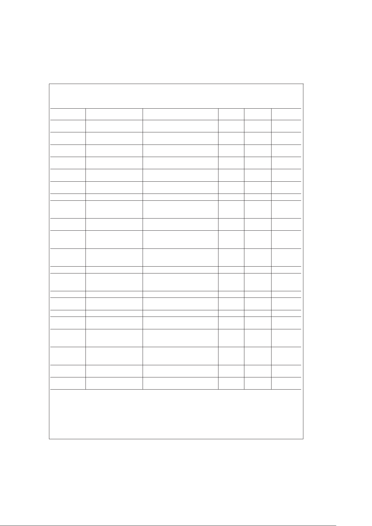
Electrical Characteristics (Continued)
Specifications with standard typeface are for T
J
=
25˚C, and those in boldface type apply over full Operating Temperature
Range.V
IN
=
10V unless otherwise specified.
Symbol Parameter Conditions
Typical
(Note 5)
Limit
(Note 4)
Units
G
M
Error Amplifier
Transconductance
1250 µmho
A
V
Error Amplifier Voltage
Gain
100
I
EA_SOURCE
Error Amplifier Source
Current
VIN= 3.6V, VFB= 1.17V, V
COMP
=
2V
40
25/15
µA
µA(min)
I
EA_SINK
Error Amplifier Sink Current VIN= 3.6V, VFB= 1.31V, V
COMP
=
2V
65
30
µA
µA(min)
V
EAH
Error Amplifier Output
Swing Upper Limit
VIN= 4V, VFB= 1.17V 2.70
2.50/2.40
V
V(min)
V
EAL
Error Amplifier Output
Swing Lower Limit
VIN= 4V, VFB= 1.31V 1.25
1.35/1.50
V
V(max)
V
D
Body Diode Voltage I
DIODE
= 1.5A 1 V
F
OSC
Oscillator Frequency Measured at Switch Pin
V
IN
=4V
300
280/255
330/345
kHz
kHz(min)
kHz(max)
D
MAX
Maximum Duty Cycle VIN=4V 95
92
%
%
(min)
I
SS
Soft-Start Current Voltage at the SS Pin = 1.4V 11
7
14
µA
µA(min)
µA(max)
V
OUTUV
V
OUT
Undervoltage
Lockout Threshold Voltage
81
76
84
%
V
OUT
%
V
OUT
(min)
%
V
OUT
(max)
Hysteresis for V
OUTUV
5
%
V
OUT
V
OUTOV
V
OUT
Overvoltage Lockout
Threshold Voltage
108
106
114
%
V
OUT
%
V
OUT
(min)
%
V
OUT
(max)
Hysteresis for V
OUTOV
3
%
V
OUT
I
LDELAY__
SOURCE
LDELAY Pin Source
Current
5µA
I
PGOOD__SINK
PGOOD Pin Sink Current V
PGOOD
= 0.4V 15 mA(max)
I
PGOOD__LEAKAGE
PGOOD Pin Leakage
Current
V
PGOOD
=5V 50 nA
I
SHUTDOWN
Shutdown Pin Current Shutdown Pin Pulled Low 2.2
0.8/0.5
3.7/4.0
µA
µA(min)
µA(max)
V
SHUTDOWN
Shutdown Pin Threshold
Voltage
Rising Edge 0.6
0.3
0.9
V
V(min)
V(max)
T
SD
Thermal Shutdown
Temperature
165 ˚C
T
SD_HYST
Thermal Shutdown
Hysteresis Temperature
25 ˚C
Note 1: Absolute Maxmum Ratingsindicate limits beyond which damageto the device may occur. Operating Ratings indicate conditionsfor which the device is intended to be functional, but device parameter specifications may notbe guaranteed under these conditions.For guaranteed specifications and test conditions, see
the Electrical Characteristics.
Note 2: The maximum allowablepower dissipation is calculated by using P
DMAX
=
(T
JMAX−TA
)/θJA, whereT
JMAX
is themaximum junction temperature, TAis the
ambient temperature, and θ
JA
is the junction-to-ambient thermal resistance of the specified package. The 893 mW rating results from using 150˚C, 25˚C, and
140˚C/W forT
JMAX,TA
, and θJArespectively.A θJAof 140˚C/W represents the worst-case condition of no heat sinkingof the 16-pin TSSOP package.Heat sinking
allows the safe dissipation of more power.The Absolute Maximum power dissipationmust bederated by7.14 mWper ˚Cabove 25˚C ambient. The LM2653 actively
limits its junction temperatures to about 165˚C.
Note 3: The human body model is a 100 pF capacitor discharged through a 1.5 kΩ resistor into each pin.
LM2653
www.national.com3
Page 4
Electrical Characteristics (Continued)
Note 4: Typical numbers are at 25˚C and represent the most likely norm.
Note 5: All limits guaranteed at room temperature (standard typeface) and at temperature extremes (bold typeface). All room temperature limits are 100%pro-
duction tested. Alllimits attemperature extremes are guaranteed viacorrelation usingstandard Statistical Quality Control (SQC) methods. All limits are used to calculate Average Outgoing Quality Level (AOQL).
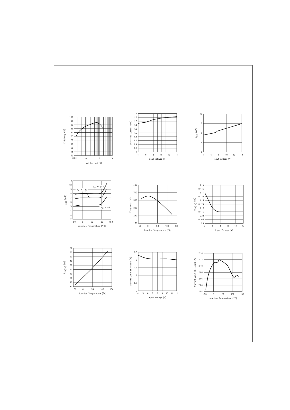
Typical Performance Characteristics
Efficiency vs Load Current
(V
IN
=
5V, V
OUT
=
2.5V)
DS101049-22
lQvs V
IN
DS101049-4
I
QSD
vs Input Voltage
DS101049-25
I
QSD
vs Junction Temperature
DS101049-26
Frequency vs Junction
Temperature
DS101049-7
R
SW(ON)
vs Input Voltage
DS101049-23
R
SW(ON)
vs Junction Temperature
DS101049-24
Current Limit vs Input Voltage
(V
OUT
=
2.5V)
DS101049-27
Current Limit vs Junction
Temperature (V
OUT
=
2.5V)
DS101049-28
LM2653
www.national.com 4
Page 5
Typical Performance Characteristics (Continued)
Connection Diagram
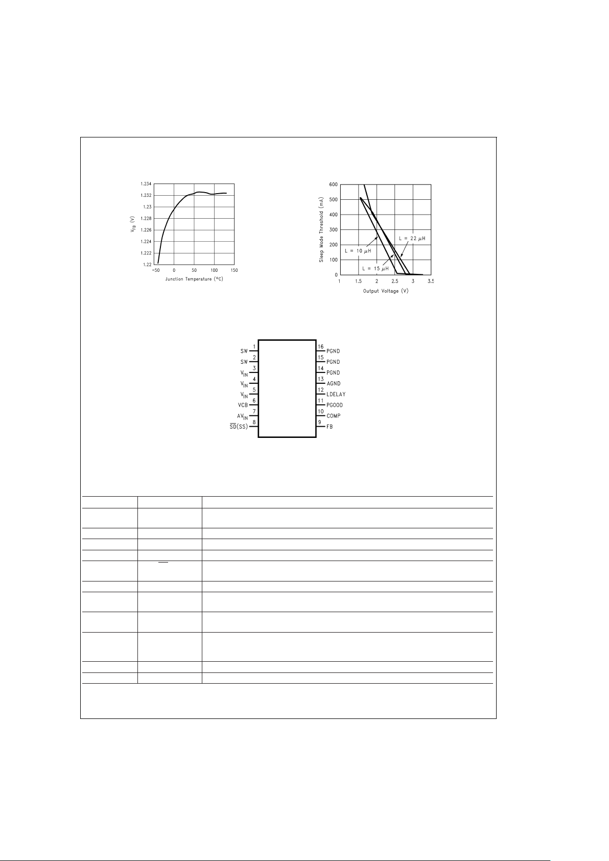
Pin Description
Pin Name Function
1-2 SW Switched-node connection, which is connected with the source of the internal high-side
MOSFET.
3-5 V
IN
Main power supply input pin. Connected to the drain of the high-side MOSFET.
6V
CB
Bootstrap capacitor connection for high-side gate drive.
7AV
IN
Input voltage for control and driver circuits.
8 SD(SS)
Shutdown control input, active low. This pin can also function as soft-start control pin.
Connect a capacitor from this pin to ground.
9 FB Output voltage feedback input. Connected to the output voltage.
10 COMP Compensation network connection. Connected to the output of the voltage error
amplifier.
11 PGOOD A constant monitor on the output voltage. PGOOD will go low if the output voltage
exceeds 110%or goes below 80%of its nominal.
12 LDELAY A capacitor between this pin to ground sets the delay from the output voltage reaches
80%of its nominal to when the undervoltage latch protection is enabled and PGOOD pin
goes low.
13 AGND Low-noise analog ground.
14-16 PGND Power ground.
Reference Voltage vs Junction Temperature
DS101049-29
Sleep Mode Threshold vs Output Voltage (V
IN
=
5V)
DS101049-31
16-Lead TSSOP (MTC)
DS101049-14
Top View
Order Number LM2653MTC-ADJ
See NS Package Number MTC16
LM2653
www.national.com5
Page 6
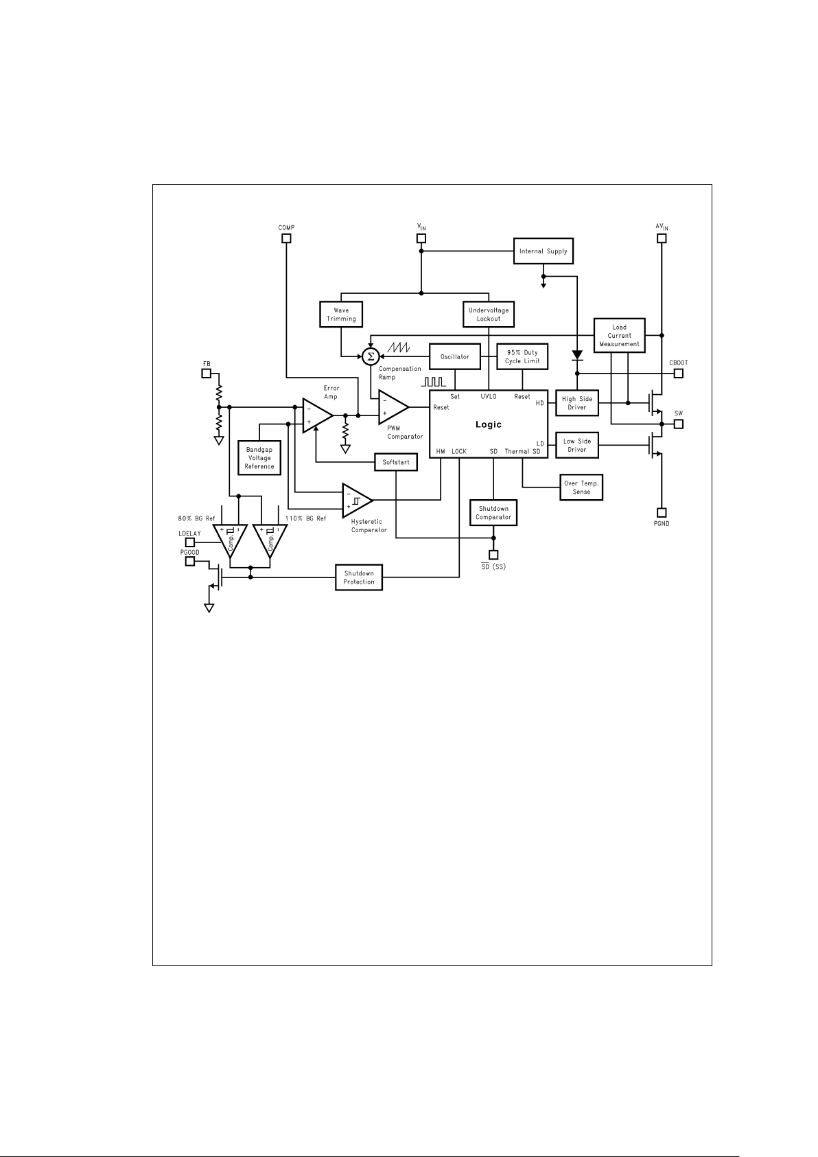
Block Diagram
Operation
The LM2653 operates in a constant frequency (300 kHz),
current-mode PWMfor moderateto heavy loads;and it automatically switches to hysteretic mode for light loads. In hysteretic mode, theswitching frequency is reducedto keep the
efficiency high.
Main Operation
When the loadcurrent is higher thanthe sleep mode threshold, thepart is always operating in PWM mode.At thebeginning of each switching cycle, the high-side switch is turned
on, thecurrent from the high-sideswitch is sensedand compared with the output of the error amplifier (COMP pin).
When the sensed current reaches the COMP pin voltage
level, the high-side switch is turned off; after 40 ns (deadtime), the low-side switch is turned on. At the end of the
switching cycle, the low-side switch is turned off; and the
same cycle repeats.
The currentof thetop switch issensed bya patented internal
circuitry.This unique techniquegets rid of the external sense
resistor, saves cost and size, and improves noise immunity
of thesensed current.Afeedforward from theinput voltageis
added to reduce thevariation of the current limit over the input voltage range.
When the load current decreases below the sleep mode
theshold, the output voltage will rise slightly, this rise is
sensed by thehysteretic mode comparator whichmakes the
part go into the hysteretic mode with both the high and low
side switchesoff. Theoutput voltage starts to dropuntil it hits
the low threshold of the hysteretic comparator, and the part
immediately goes back to the PWM operation. The output
voltage keeps increasing until it reaches the top hysteretic
threshold, then both the high and low side switches turn off
again, and th same cycle repeats.
Protections
The cycle-by-cycle current limit circuitry turns off the
high-side MOSFET whenever the current in MOSFET
reaches 2A. A second level current limit is accomplished by
the undervoltage protection: if the load pulls the output voltage down below 80%of its nominal value, the undervoltage
latch protection will wait for a period of time (set by the capacitor at the LDELAY pin, see LDELAY CAPACITOR section for more information). If the output voltage is still below
80%of its nominal after the waiting period, the latch protection will be enabled. In the latch protection mode, the
low-side MOSFET is on and the high-side MOSFET is off.
The latch protection will also be enabled immediately whenever the output voltage exceeds the overvoltage threshold
(110%of its nominal). Both protections are disabled during
start-up.(See SOFT-START CAPACITOR section and LDELAYCAPACITORsection for moreinformation.) Toggling the
input supply voltage or the shutdown pin can reset the device from the latched protection mode.
DS101049-15
LM2653
www.national.com 6
Page 7
Operation (Continued)
PGOOD Flag
The PGOOD flag goes low whenever the overvoltage or undervoltage latch protection is enabled.
DESIGN PROCEDURE
This section presents guidelines for selecting external components.
INPUT CAPACITOR
A low ESR aluminum, tantalum, or ceramic capacitor is
needed betwenthe input pinand power ground.This capacitor prevents large voltage transients from appearing at the
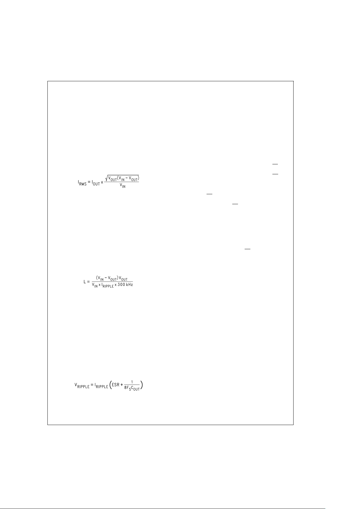
input. The capacitor is selected based on the RMS current
and voltage requirements. The RMS current is given by:
The RMS current reaches its maximum (I
OUT
/2) when
V
IN
equals 2V
OUT
. For an aluminum or ceramic capacitor,
the voltage rating should be at least 25%higher than the
maximum input voltage. If a tantalum capacitor is used, the
voltage rating required is about twice the maximum input
voltage. The tantalum capacitor should be surge current
tested by the manufacturer to prevent shorted by the inrush
current. It is also recommended to put a small ceramic capacitor (0.1 µF) between the input pin and ground pin to reduce high frequency spikes.
INDUCTOR
The most critical parameters for the inductor are the inductance, peak current and the DC resistance. The inductance
is related to the peak-to-peak inductor ripple current, the input and the output voltages:
A higher value of ripple current reduces inductance, but increases the conductance loss, core loss, current stress for
the inductorand switch devices. It alsorequires a biggeroutput capacitorfor the same output voltage ripple requirement.
A reasonable value is setting the ripple current to be 30%of
the DC output current. Since the ripple current increases
with the input voltage, the maximum input voltage is always
used to determine the inductance.The DC resistance of the
inductor is a key parameter for the efficiency. Lower DC resistance is available with a bigger winding area. A good
tradeoff between the efficiencyand thecore sizeis lettingthe
inductor copper loss equal 2%of the output power.
OUTPUT CAPACITOR
The selection of C
OUT
is driven by the maximum allowable
output voltage ripple. The output ripple in the constant frequency, PWM mode is approximated by:
The ESRterm usuallyplays the dominantrole in determining
the voltage ripple.A low ESR aluminum electrolytic or tantalum capacitor (such as Nichicon PL series, Sanyo OS-CON,
Sprague 593D, 594D, AVX TPS, and CDE polymer aluminum) is recommended. An electrolytic capacitor is not recommended for temperatures below −25˚C since its ESR
rises dramatically at cold temperature. A tantalum capacitor
has amuch betterESR specification at cold temperatureand
is preferred for low temperature applications.
The output voltageripple in constant frequency modehas to
be less than the sleep mode voltage hysteresis to avoid entering the sleep mode at full load:
V
RIPPLE
<
20mV*V
OUT/VFB
BOOST CAPACITOR
A0.1 µFceramic capacitor isrecommended forthe boostcapacitor. The typical voltage across the boost capacitor is
6.7V.
SOFT-START CAPACITOR
Asoft-start capacitor is usedto provide thesoft-start feature.
When the input voltage is first applied, or when the SD(SS)
pin is allowed to go high, the soft-start capacitor is charged
by a currentsource (approximately 2 µA). Whenthe SD(SS)
pin voltage reaches 0.6V (shutdown threshold), the internal
regulator circuitry startsto operate. The currentcharging the
soft-start capacitor increases from 2 µA to approximately
10 µA. With theSD(SS) pin voltage between 0.6V and 1.3V,
the level of the current limit is zero, which means the output
voltage is still zero. When the SD(SS) pin voltage increases
beyond 1.3V, the current limit starts to increase. The switch
duty cycle,which iscontrolled by thelevel ofthe current limit,
starts with narrow pulses and gradually gets wider. At the
same time, the output voltage of the converter increases towards the nominal value, which brings down the output voltage ofthe error amplifier. Whenthe output of the erroramplifier is less than the current limit voltage, it takes over the
control of the duty cycle. The converter enters the normal
current-mode PWM operation. The SD(SS) pin voltage is
eventually charged up to about 2V.
The soft-start time can be estimated as:
T
SS
=
C
SS
*
0.6V/2 µA + C
SS
*
(2V−0.6V)/10 µA
During start-up,the internal circuitis monitoring thesoft-start
voltage. When the softstart voltage reaches 2V, the undervoltage and overvoltage protections are enabled.
If the output voltage doesn’t rise above 80%of the normal
value before the soft-start reaches 2V. The undervoltage
protection will kick in and shut the device down. You can
avoid this by either increasing the value of the soft-start capacitor, or using a LDELAY capacitor.
LDELAY CAPACITOR
As mentioned in the operation section, the LDELAY capacitor sets the time delay between the output voltage goes below 80%of itsnominal value and theundervoltage latch protection is enabled.
Charging the CDELAY bya5µAcurrent source up to 2V
sets the delay time. Therefore, T
DELAY
=
C
DELAY
*
2V/5µA.
The undervoltageprotection isdisabled by tyingthe LDELAY
pin to the ground.
R
1
and R2(Programming Output Voltage)
Use the following formula to select the appropriate resistor
values:
V
OUT
=
V
REF
(1+R1/R2)
where V
REF
=
1.238V
Select resistorsbetween 10kΩand 100kΩ.(1%or higheraccuracy metal film resistors for R
1
and R2.)
LM2653
www.national.com7
Page 8
DESIGN PROCEDURE (Continued)
COMPENSATION COMPONENTS
In thecontrol tooutput transferfunction, the firstpole F
p1
can
be estimated as 1/(2πR
OUTCOUT
); The ESR zero Fz1of the
output capacitor is 1/(2πESRC
OUT
); Also,there is a high fre-
quency pole F
p2
in the range of 45kHz to 150kHz:
F
p2
=
F
s
/(πn(1−D))
where D=V
OUT/VIN
,n=1+0.348L/(VIN−V
OUT
)(LisinµHs
and V
IN
and V
OUT
in volts).
The total loop gain G is approximately 500/I
OUT
where I
OUT
is in amperes.
A Gmamplifier is used inside the LM2653.The output resis-
tor R
o
of the Gm amplifier is about 80kΩ.Cc1and RCto-
gether with R
o
give a lag compensation to roll off the gain:
F
pc1
=
1/(2πC
c1(Ro+Rc
)), F
zc1
=
1/2πC
c1Rc
.
In someapplications, the ESRzero F
z1
can notbe cancelled
by F
p2
. Then, Cc2is needed to introduce F
pc2
to cancel the
ESR zero, F
p2
=
1/(2πC
c2Ro\Rc
).
The rule of thumb is to have more than 45˚ phase margin at
the crossover frequency (G=1).
If C
OUT
is higherthan 68µF, C
c1
=
2.2nF, andR
c
=
15KΩ are
good choices for most applications. If the ESR zero is too
low to be cancelled by F
p2
, add Cc2.
If the transient response to a step load is important, choose
R
C
to be higher than 10kΩ.
EXTERNAL SCHOTTKY DIODE
A Schottky diode D
1
is recommended toprevent the intrinsic
body diode of thelow-side MOSFET from conducting during
the deadtime in PWM operation and hysteretic mode when
both MOSFETs are off. If the body diode turns on, there is
extra power dissipation in the body diode because of the
reverse-recovery current and higher forward voltage; the
high-side MOSFET also has more switching loss since the
negative diode reverse-recovery current appears as the
high-side MOSFET turn-on current in addition to the load
current. These losses degrade the efficiency by 1-2%. The
improved efficiencyand noise immunity withthe Schottky diode become moreobvious with increasing input voltageand
load current.
The breakdown voltage rating of D
1
is preferred to be 25
%
higher than the maximum input voltage. Since D
1
is only on
for a short period of time, the average current rating for D
1
only requires being higher than 30%of the maximum output
current. Itis important toplace D
1
very closeto the drainand
source of the low-side MOSFET, extra parasitic inductance
in the parallel loop will slow the turn-on of D
1
and direct the
current through the body diode of the low-side MOSFET.
PCB LAYOUT CONSIDERATIONS
Layout is critical to reduce noises and ensure specified performance. The important guidelines are listed as follows:
1. Minimize the parasitic inductance in theloop of input ca-
pacitors andthe internal MOSFETs byconnecting theinput capacitorsto V
IN
and PGNDpins withshort and wide
traces. This is important because the rapidly switching
current, together with wiring inductance can generate
large voltage spikes that may result in noise problems.
2. Minimize the trace from the center of the output resistor
divider to the FB pin and keep it away from noise
sources to avoid noise pick up. For applications require
tight regulation at the output, a dedicated sense trace
(separated from the power trace) is recommended to
connect the top of the resistor divider to the output.
3. If the Schottky diode D
1
is used, minimize the traces
connecting D
1
to SW and PGND pins.
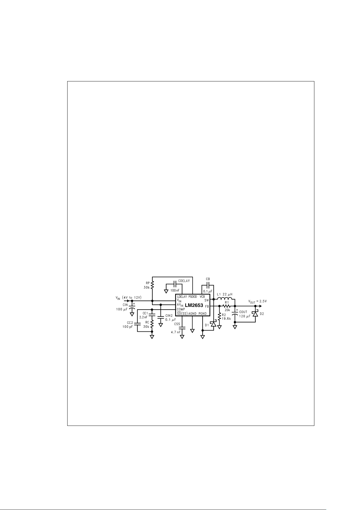
DS101049-1
Schematic for the Typical Board Layout
LM2653
www.national.com 8
Page 9
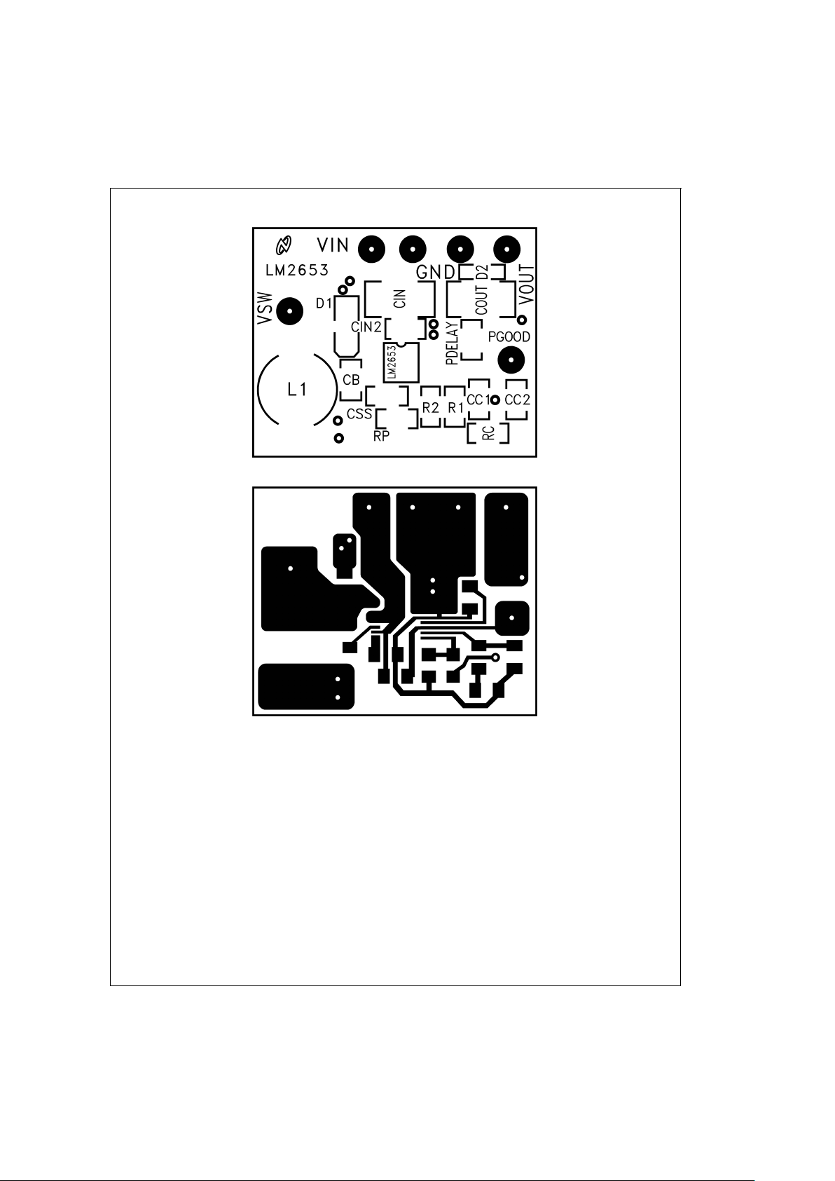
Typical PC Board Layout: (2X Size)
DS101049-19
Component Placement Guide
DS101049-20
Component Side PC Board Layout
LM2653
www.national.com9
Page 10
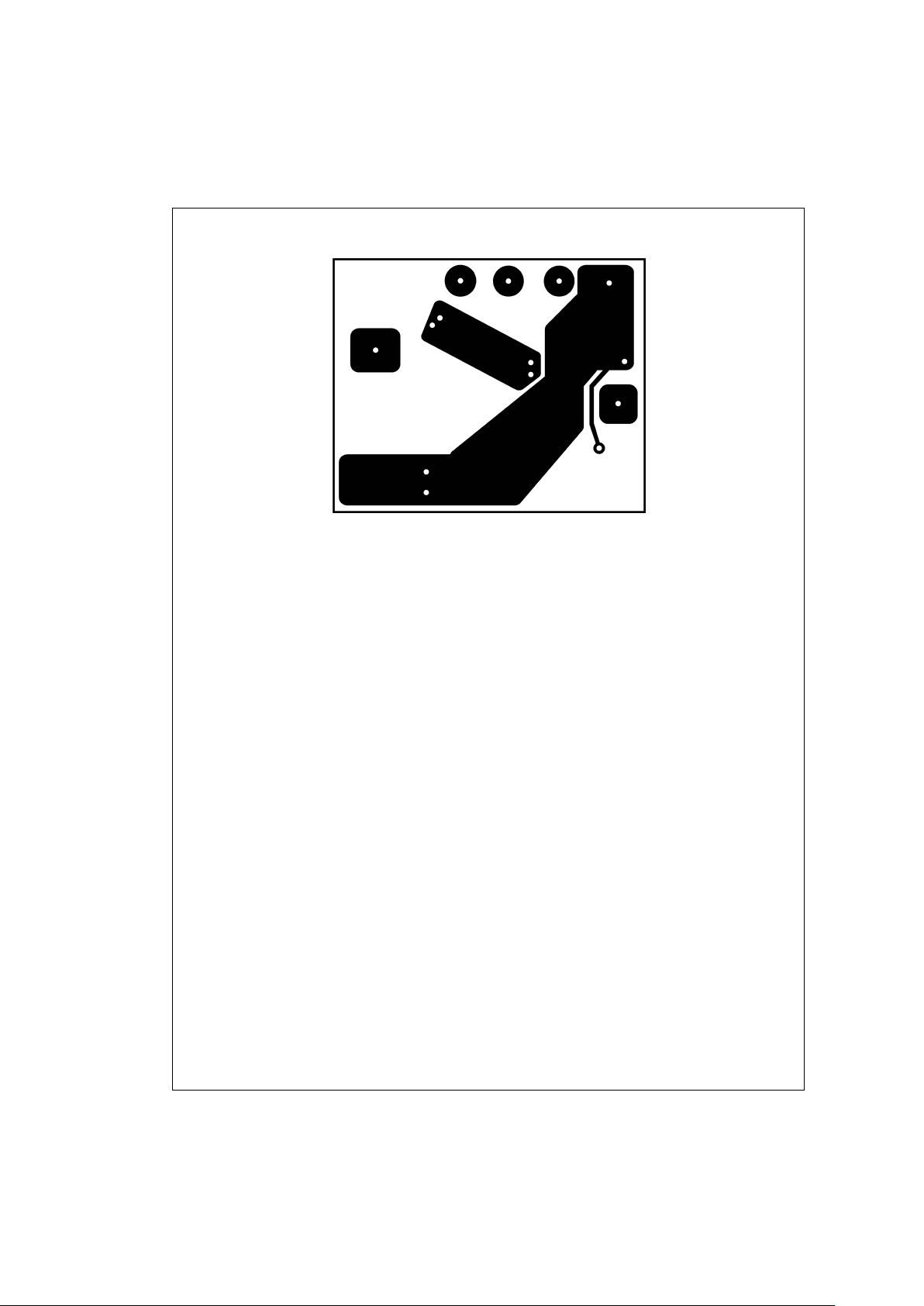
Typical PC Board Layout: (2X Size) (Continued)
DS101049-21
Solder Side PC Board Layout
LM2653
www.national.com 10
Page 11
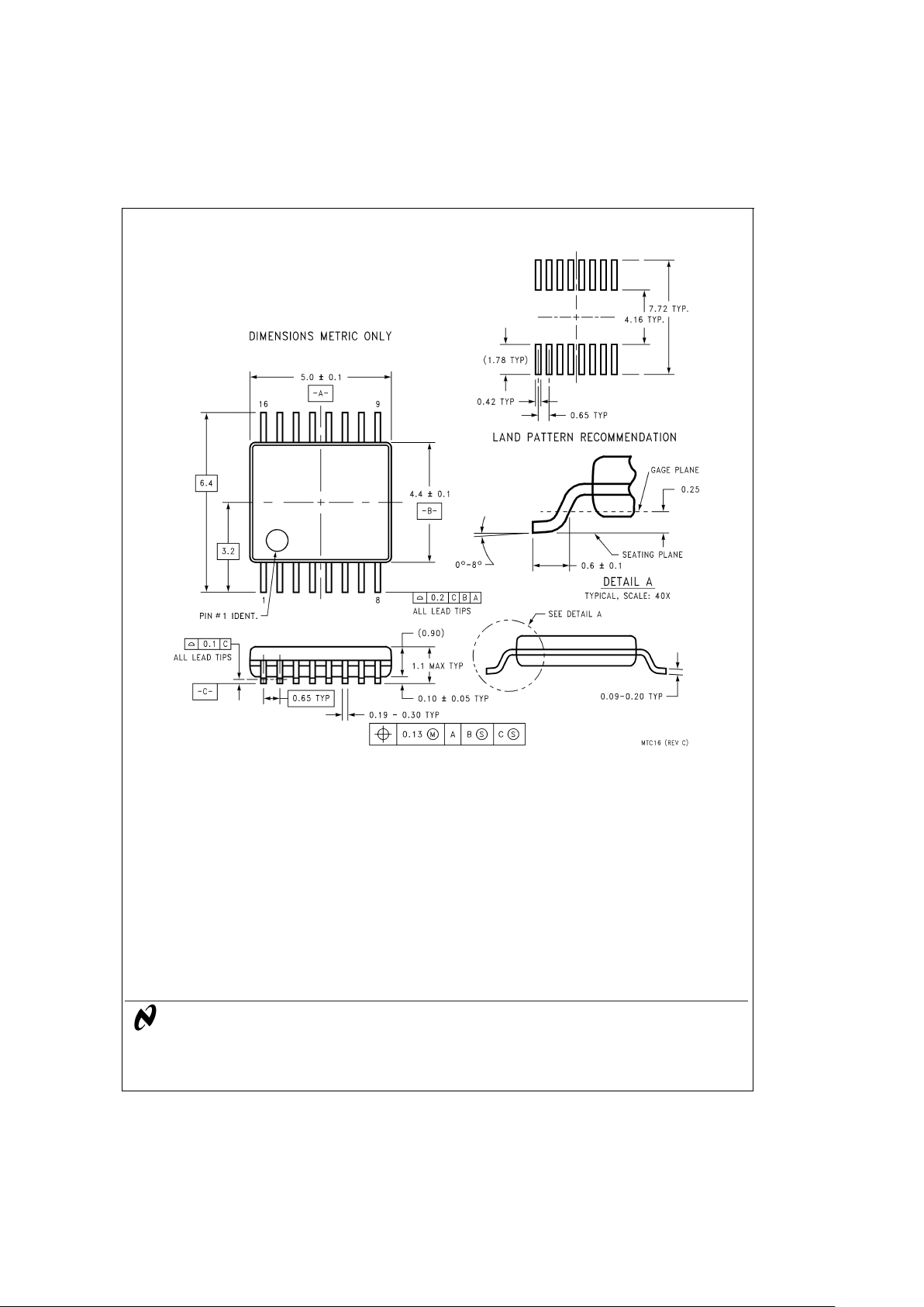
Physical Dimensions inches (millimeters) unless otherwise noted
LIFE SUPPORT POLICY
NATIONAL’S PRODUCTS ARE NOT AUTHORIZED FOR USE AS CRITICAL COMPONENTS IN LIFE SUPPORT
DEVICES OR SYSTEMS WITHOUT THE EXPRESS WRITTEN APPROVAL OF THE PRESIDENT AND GENERAL
COUNSEL OF NATIONAL SEMICONDUCTOR CORPORATION. As used herein:
1. Life support devices or systems are devices or
systems which, (a) are intended for surgical implant
into the body, or (b) support or sustain life, and
whose failure to perform when properly used in
accordance with instructions for use provided in the
labeling, can be reasonably expected to result in a
significant injury to the user.
2. A critical component is any component of a life
support device or system whose failure to perform
can be reasonably expected to cause the failure of
the life support device or system, or to affect its
safety or effectiveness.
National Semiconductor
Corporation
Americas
Tel: 1-800-272-9959
Fax: 1-800-737-7018
Email: [email protected]
National Semiconductor
Europe
Fax: +49 (0) 1 80-530 85 86
Email: [email protected]
Deutsch Tel: +49 (0)1 80-530 85 85
English Tel: +49 (0) 1 80-532 78 32
Français Tel: +49 (0) 1 80-532 93 58
Italiano Tel: +49 (0) 1 80-534 16 80
National Semiconductor
Asia Pacific Customer
Response Group
Tel: 65-2544466
Fax: 65-2504466
Email: [email protected]
National Semiconductor
Japan Ltd.
Tel: 81-3-5639-7560
Fax: 81-3-5639-7507
www.national.com
16-Lead TSSOP (MTC)
Order Number LM2653MTC-ADJ
NS Package Number MTC16
LM2653 1.5A High Efficiency Synchronous Switching Regulator
National does not assume any responsibility for use of any circuitry described, no circuitpatent licenses are implied and National reserves the right at any timewithout notice to change said circuitry and specifications.
 Loading...