

Page 1
LM2647
Dual Synchronous Buck Regulator Controller
General Description
The LM2647 is an adjustable 200-500kHz dual channel
voltage-mode controlled high-speed synchronous buck
regulator controller ideally suited for battery powered applications such as laptop and notebook computers. The
LM2647 requires only N-channel FETs for both the upper
and lower positions of each synchronous stage. It features
line feedforward to improve the response to input transients.
At very light loads, the user can choose between the highefficiency Pulse-skip mode or the constant frequency
Forced-PWM mode. Lossless current limiting without the use
of external sense resistors is made possible by sensing the
voltage drop across the bottom FET. A unique adaptive duty
cycle clamping technique is incorporated to significantly reduce peak currents under abnormal load conditions. The two
independently programmable outputs switch 180˚ out of
phase (interleaved switching) to reduce the input capacitor
and filter requirements. The input voltage range is 5.5V to
28V while the output voltages are adjustable down to 0.6V.
Standard supervisory and control features include Soft-start,
Power Good, output Under-voltage and Over-voltage protection, Under-voltage Lockout, Soft-shutdown and Enable.
Features
n Input voltage range from 5.5V to 28V
n Synchronous dual-channel Interleaved switching
n Forced-PWM or Pulse-skip modes
n Lossless bottom-side FET current sensing
n Adaptive duty cycle clamping
n High current N-channel FET drivers
n Low shutdown supply currents
n Reference voltage accurate to within
±
1.5%
n Output voltage adjustable down to 0.6V
n Power Good flag and Chip Enable
n Under-voltage lockout
n Over-voltage/Under-voltage protection
n Soft-start and Soft-shutdown
n Switching frequency adjustable 200kHz-500kHz
Applications
n Notebook Chipset Power Supplies
n Low Output Voltage High-Efficiency Buck Regulators
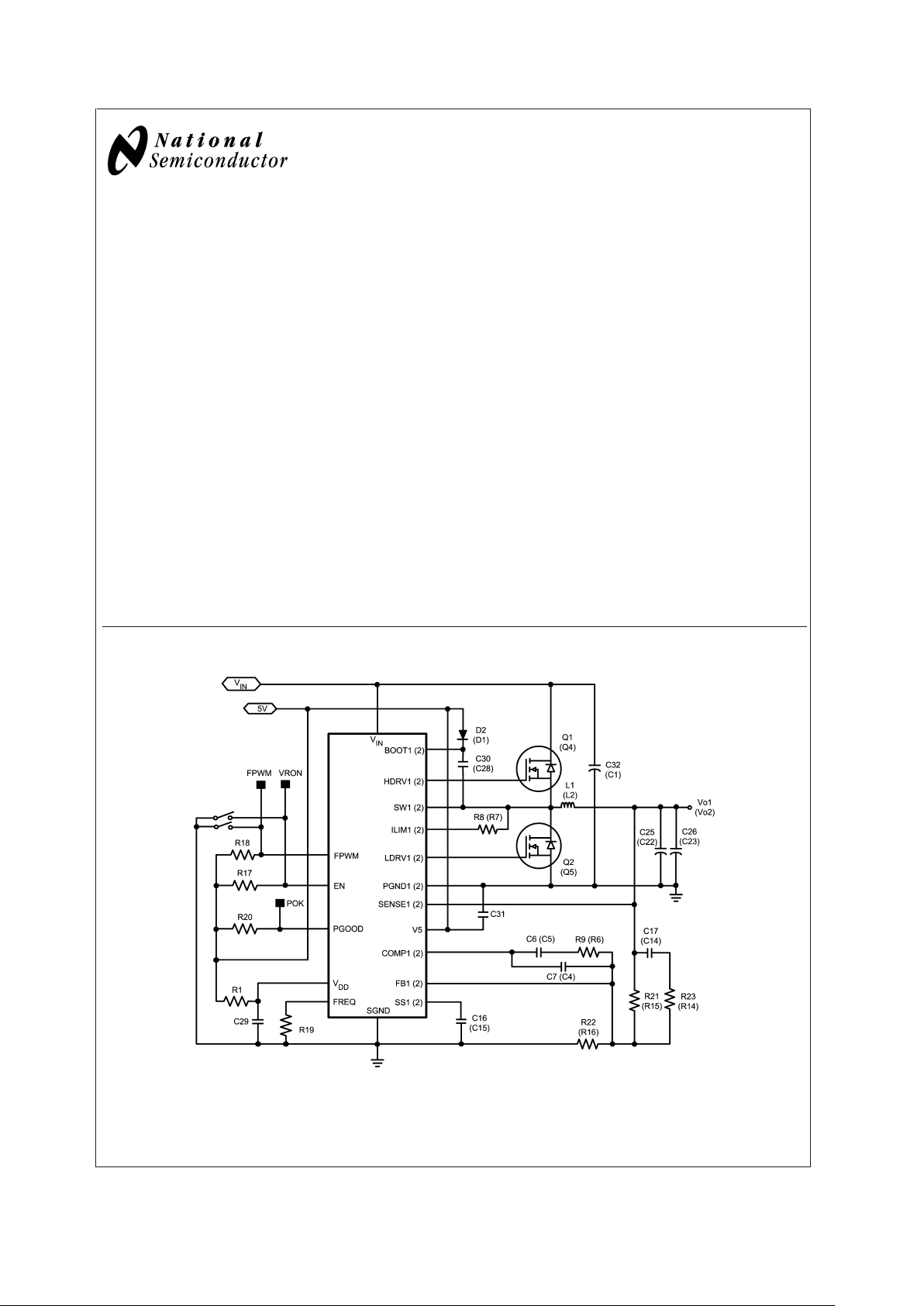
Typical Application (Channel 2 in parenthesis)
20056304
June 2003
Dual Synchronous Buck Regulator Controller
© 2003 National Semiconductor Corporation DS200563 www.national.com
Page 2
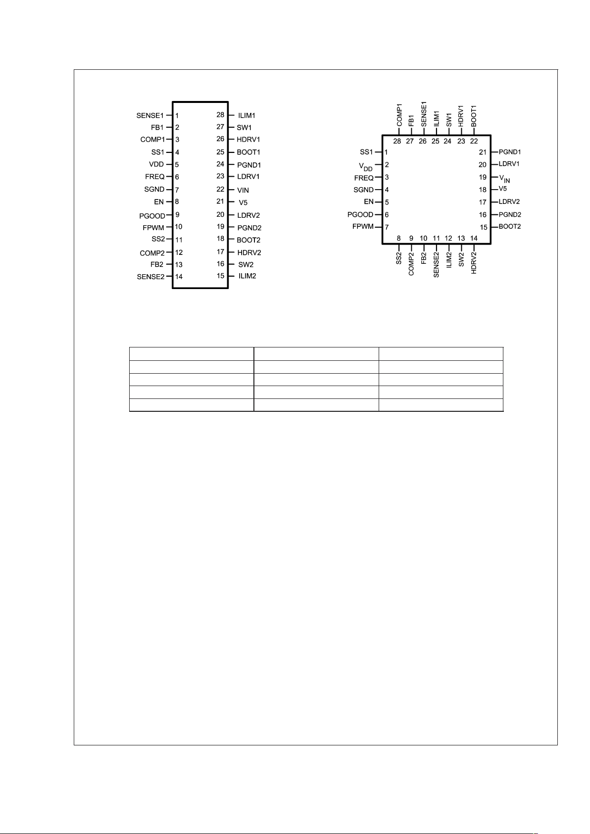
Connection Diagrams
20056302
Top View
28-Lead TSSOP (MTC)
20056303
Top View
28-Lead LLP (LQA)
Ordering Information
Order Number Package Drawing Supplied As
LM2647MTC MTC28 48 Units/Rail
LM2647MTCX MTC28 2500 Units/13" Reel
LM2647LQ LQA28A 1000 Units/7" Reel
LM2647LQX LQA28A 4500 Units/13" Reel
Pin Description
(All pin numbers referred to here correspond to the TSSOP
package)
Pin 1, SENSE1: Output voltage sense pin for Channel 1. It is
tied directly to the output rail. The SENSE pin voltage is used
together with the VIN voltage (on Pin 22) to (internally)
calculate the CCM (continuous conduction mode) duty cycle.
This calculation is used by the IC to set the minimum duty
cycle in the SKIP mode to 85% of the CCM value. It is also
used to set the adaptive duty cycle clamp (see Pin 3). An
internal 20Ω resistor from the SENSE pin to ground discharges the output capacitor gently (Soft-shutdown) whenever Power Not Good is signaled on Pin 9.
Pin 2, FB1: Feedback pin for Channel 1. This is the inverting
input of the error amplifier. The voltage on this pin under
regulation is nominally at 0.6V. A Power Good window on this
pin determines if the output voltage is within regulation limits
(
±
13%). If the voltage (on either channel) falls outside this
window for more than 7µs, Power Not Good is signaled on
the PGOOD pin (Pin 9). Output over-voltage and undervoltage conditions are also detected by comparing the voltage on the Feedback pin with appropriate internal reference
voltage levels. If the voltage exceeds the safe window
(
±
30%) for longer than 7µs, a fault condition is asserted.
Then both the lower FETs are latched ON and the upper
FETs are latched OFF. When single channel operation is
desired, the Feedback pins of both channels should be
connected together, near the IC. All other pins specific to the
unused channel should be left floating (not connected to
each other either).
Pin 3, COMP1: Compensation pin for Channel 1. This is also
the output of the error amplifier of this channel. The voltage
level on this pin is compared with an internally generated
ramp signal to set the duty cycle for normal regulation. Since
the Feedback pin is the inverting input of the same error
amplifier, appropriate control loop compensation components are placed between this pin and the Feedback pin.
The COMP pin is internally pulled low during Soft-start so as
to limit the duty cycle. Once Soft-start is completed, the
voltage on this pin can take up the value required to maintain
output regulation. But an internal voltage clamp does not
allow the pin to go much higher than the steady-state requirement. This forms the adaptive duty cycle clamp feature
which serves to limit the maximum allowable duty cycle and
peak currents under sudden overloads. But at the same time
it has enough headroom to permit an adequate response to
step loads within the normal operating range.
Pin 4, SS1: Channel 1 Soft-start pin. A Soft-start capacitor is
placed between this pin and ground. A typical capacitance of
0.1µF is always recommended between this pin and ground.
The IC connects an internal 1.8 kΩ resistor (R
SS_DCHG
, see
Electrical Characteristics table) between this pin and ground
to discharge any remaining charge on the Soft-start capacitor under several conditions. These conditions include the
initial power-up sequence, start-up by toggling the EN pin,
and also recovery from a fault condition. The purpose is to
bring down the voltage on both the Soft-start pins to below
100mV for obtaining reset. Reset having thus been obtained,
an 11µA current source at this pin charges up the Soft-start
capacitor. The voltage on this pin controls the maximum duty
cycle, and this produces a gradual ramp-up of the output
voltage, thereby preventing large inrush currents into the
LM2647
www.national.com 2
Page 3

Pin Description (Continued)
output capacitors. The voltage on this pin finally clamps
close to 5V. This pin is again connected to the internal 115µA
current sink whenever a current limit event is in progress.
This sink current discharges the Soft-start capacitor and
forces the duty cycle low to protect the power components.
When a fault condition is asserted (See Pin 2) the SS pin is
internally connected to ground via the 1.8 kΩ resistor.
Pin 5, VDD: 5V supply rail for the control and logic sections
of both channels. For normal operation to start, the voltage
on this pin must be brought above 4.5V. Subsequently, the
voltage on this pin (including any ripple component) should
not allowed to fall below 4V for a duration longer than 7µs.
Since this pin is also the supply rail for the internal control
sections, it should be well-decoupled particularly at high
frequencies. A minimum 0.1µF-0.47µF (ceramic) capacitor
should be placed on the component side very close to the IC
with no intervening vias between this capacitor and the
VDD/SGND pins. If the voltage on Pin 5 falls below the lower
UVLO threshold, both upper FETs are latched OFF and
lower FETs latched ON. Power Not Good is then also signaled immediately (on Pin 9). To effect recovery, the EN pin
must be taken below 0.8V and then back above 2V (with
VDD held above 4.5V). Or the voltage on the VDD pin must
be taken below 1.0V and then back again above 4.5V (with
EN pin held above 2V). Normal operation will then resume
assuming that the fault condition has cleared.
Pin 6, FREQ: Frequency adjust pin. The switching frequency
(for both channels) is set by a resistor connected between
this pin and ground. A value of 22.1kΩ sets the frequency to
300kHz (nominal). If the resistance is increased, the switching frequency falls. An approximate relationship is that for
every 7.3kΩ increase (or decrease) in the value of the frequency adjust resistance, the time period (1/f) increases (or
decreases) by about 1µs.
Pin 7, SGND: Signal Ground pin. This is the lower rail for the
control and logic sections of both channels. SGND should be
connected on the PCB to the system ground, which in turn is
connected to PGND1 and PGND2. The layout is important
and the recommendations in the section Layout Guidelines
should be followed.
Pin 8, EN: IC Enable pin. When EN is taken high, both
channels are enabled by means of a Soft-start power-up
sequence (see Pin 4). When EN is brought low, Power Not
Good is signaled within 100ns. This causes Soft-shutdown to
occur (see Pins 1 and 9). The Soft-start capacitor is then
discharged by an internal 1.8kΩ resistor (R
SS_DCHG
, see
Electrical Characteristics table). But note that when the Enable pin is toggled, a fault condition is not asserted. Therefore in this case, the lower FETs are not latched ON, even as
the output voltage ramps down, eventually falling below the
under-voltage threshold. In fact, in this situation, both the
upper and the lower FETs of the two channels are latched
OFF, until the Enable pin is taken high again. If a fault
shutdown has occurred, taking the Enable pin low and then
high again (toggling), resets the internal latches, and the IC
will resume normal switching operation.
Pin 9, PGOOD: Power Good output pin. An open-Drain logic
output that is pulled high with an external pull-up resistor,
indicating that both output voltages are within a pre-defined
Power Good window. Outside this window, the pin is internally pulled low (Power Not Good signaled) provided the
output error lasts for more than 7µs. But the pin is also pulled
low within 100ns of the Enable pin being taken low, irrespective of the output voltage level. Note that PGOOD must
always be high before it can respond by going low. So
regulation on both channels must be achieved first. Further,
for fault monitoring to be in place, PGOOD must have been
high prior to occurrence of the fault condition. Note that since
under a fault assertion, the lower FETs are always latched
ON, this will not happen if regulation has not been already
been achieved first. For correct signaling on this pin under
single-channel operation, see description of Pin 2.
Pin 10, FPWM: Logic input for selecting either the Forced
PWM (FPWM) Mode or Pulse-skip Mode (SKIP) for both
channels (together). When the pin is driven high, the IC
operates in the FPWM mode, and when pulled low or left
floating, the SKIP mode is enabled. In FPWM mode, the
lower FET of a given channel is always ON whenever the
upper FET is OFF (except for a narrow shoot-through protection deadband). This leads to continuous conduction
mode of operation, which has a fixed frequency and (almost)
fixed duty cycle down to very light loads. But this does
reduce efficiency at light loads. The alternative is the SKIP
mode, where the lower FET remains ON only until the voltage on the Switch pin (see Pin 27 or Pin 16) is more negative
than 2.2mV (typical). So for example, for a 21mΩ FET, this
translates to a current threshold of 2.2mV/21mΩ = 0.1A.
Therefore, if the (instantaneous) inductor current falls below
this value, the lower FET will turn OFF every cycle at this
point (when operated in SKIP mode). This threshold is set by
the zero-cross Comparator in the Block Diagram. Note that if
the inductor current waveform is high enough to be always
above this zero-cross threshold (V
SW_ZERO
, see Table of
Electrical Characteristics), there will be no observable difference between FPWM and SKIP mode settings (in steadystate). SKIP mode, when it actually occurs, is clearly a
discontinuous mode of operation. However, note that in conventional discontinuous mode, the duty cycle keeps falling
(towards zero) as the load decreases. But the LM2647 does
not allow the duty cycle to fall by more than 15% of its
original value (at the CCM-DCM boundary). This forces
pulse-skipping, and the average frequency is effectively decreased as the load decreases. This mode of operation
improves efficiency at light loads, but the frequency is effectively no longer a constant. Note that a minimum pre-load of
0.1mA should be maintained on the output of each channel
to ensure regulation in SKIP mode. The resistive divider from
output to ground used to set the output voltage could be
designed to serve as part or all of this required pre-load.
Pin 11, SS2: Soft-start pin for Channel 2. See Pin 4.
Pin 12, COMP2: Soft-start pin for Channel 2. See Pin 3.
Pin 13, FB2: Feedback pin for Channel 2. See Pin 2.
Pin 14, SENSE2: Output voltage sense pin for Channel 2.
See Pin 1.
Pin 15, ILIM2: Channel 2 Current Limit pin. When the bottom
FET is ON, a 62µA (typical) current flows out of this pin into
an external current limit setting resistor connected to the
Drain of the lower FET. This is a current source, therefore the
drop across this resistor serves to push the voltage on this
pin to a more positive value. However, the Drain of the lower
FET which is connected to the other side of the same
resistor is trying to go more negative as the load current
increases. At some value of instantaneous current, the voltage on this pin will transit from positive to negative. The point
where it is zero is the current limiting condition and is detected by the Current Limit Comparator in the Block Diagram. When current limit condition has been detected, the
next ON-pulse of the upper FET will be omitted. The lower
FET will again be monitored to determine if the current has
fallen below the threshold. If it has, the next ON-pulse will be
LM2647
www.national.com3
Page 4

Pin Description (Continued)
permitted. If not, the upper FET will be turned OFF and will
stay so for several cycles if necessary, until the current
returns to normal. Eventually, if the overcurrent condition
persists, and the upper FET has not been turned ON, the
output will clearly start to fall. Ultimately the output will fall
below the under-voltage threshold, and a fault condition will
be asserted by the IC.
Pin 16, SW2: The Switching node of the buck regulator of
Channel 2. Also serves as the lower rail of the floating driver
of the upper FET.
Pin 17, HDRV2: Gate drive pin for the upper FET of Channel
2 (High-side drive). The top gate driver is interlocked with the
bottom gate driver to prevent shoot-through/crossconduction.
Pin 18, BOOT2: Bootstrap pin for Channel 2. This is the
upper supply rail for the floating driver of the upper FET. It is
bootstrapped by means of a ceramic capacitor connected to
the channel Switching node. This capacitor is charged up by
the IC to a value of about 5V as derived from the V5 pin (Pin
21).
Pin 19, PGND2: Power Ground pin of Channel 2. This is the
return path for the bottom FET gate drive. Both the PGND’s
are to be connected on the PCB to the system ground and
also to the Signal ground (Pin 7) in accordance with the
recommended Layout Guidelines .
Pin 20, LDRV2: Gate drive pin for the Channel 2 bottom FET
(Low-side drive). The bottom gate driver is interlocked with
the top gate driver to prevent shoot-through/crossconduction. It is always latched high when a fault condition is
asserted by the IC.
Pin 21, V5: Upper rail of the lower FET drivers of both
channels. Also used to charge up the bootstrap capacitors of
the upper FET drivers. This is connected to an external 5V
supply. The 5V rail may be the same as the rail used to
provide power to the VDD pin (Pin 5), but the VDD pin will
then require to be well-decoupled so that it does not interact
with the V5 pin. A low-pass RC filter consisting of a ceramic
0.1µF capacitor (preferably 0.22µF) and a 10Ω resistor will
suffice as shown in the Typical Applications circuit.
Pin 22, VIN: The input to both the Buck regulator power
stages. It also is used by the internal ramp generator to
implement the line feedforward feature. The VIN pin is also
used with the SENSE pin voltage to predict the CCM (continuous conduction mode) duty cycle and to thereby set the
minimum allowed DCM duty cycle to 85% of the CCM value
(in SKIP mode, see Pin 10). This is a high input impedance
pin, drawing only about 100µA (typical) from the input rail.
Pin 23, LDRV1: LDRV pin of Channel 1. See Pin 20.
Pin 24, PGND1: PGND pin for Channel 1.See Pin 19.
Pin 25, BOOT1: Boot pin of Channel 1. See Pin 18.
Pin 26, HDRV1: HDRV pin of Channel 1. See Pin 17.
Pin 27, SW1: SW pin of Channel 1. See Pin 16.
Pin 28, ILIM1: Channel 2 Current Limit pin. See Pin 15.
LM2647
www.national.com 4
Page 5
Absolute Maximum Ratings (Note 1)
If Military/Aerospace specified devices are required,
please contact the National Semiconductor Sales Office/
Distributors for availability and specifications.
Voltages from the indicated pins to SGND/PGND unless
otherwise indicated (Note 2):
VIN 30V
V5 7V
VDD 7V
BOOT1, BOOT2 36V
BOOT1 to SW1, BOOT2 to
SW2 7V
SW1, SW2 30V
ILIM1, ILIM2 30V
SENSE1, SENSE2, FB1, FB2 7V
PGOOD 7V
EN 7V
Power Dissipation (T
A
= 25˚C)
(Note 3) 1.0W
Junction Temperature +150˚C
ESD Rating (Note 4) 2kV
Ambient Storage Temperature
Range -65˚C to +150˚C
Soldering Dwell Time,
Temperature
Wave
Infrared
Vapor Phase
4 sec, 260˚C
10 sec, 240˚C
75 sec, 219˚C
Operating Ratings (Note 1)
VIN 5.5V to 28V
VDD, V5 4.5V to 5.5V
Junction Temperature -5˚C to +125˚C
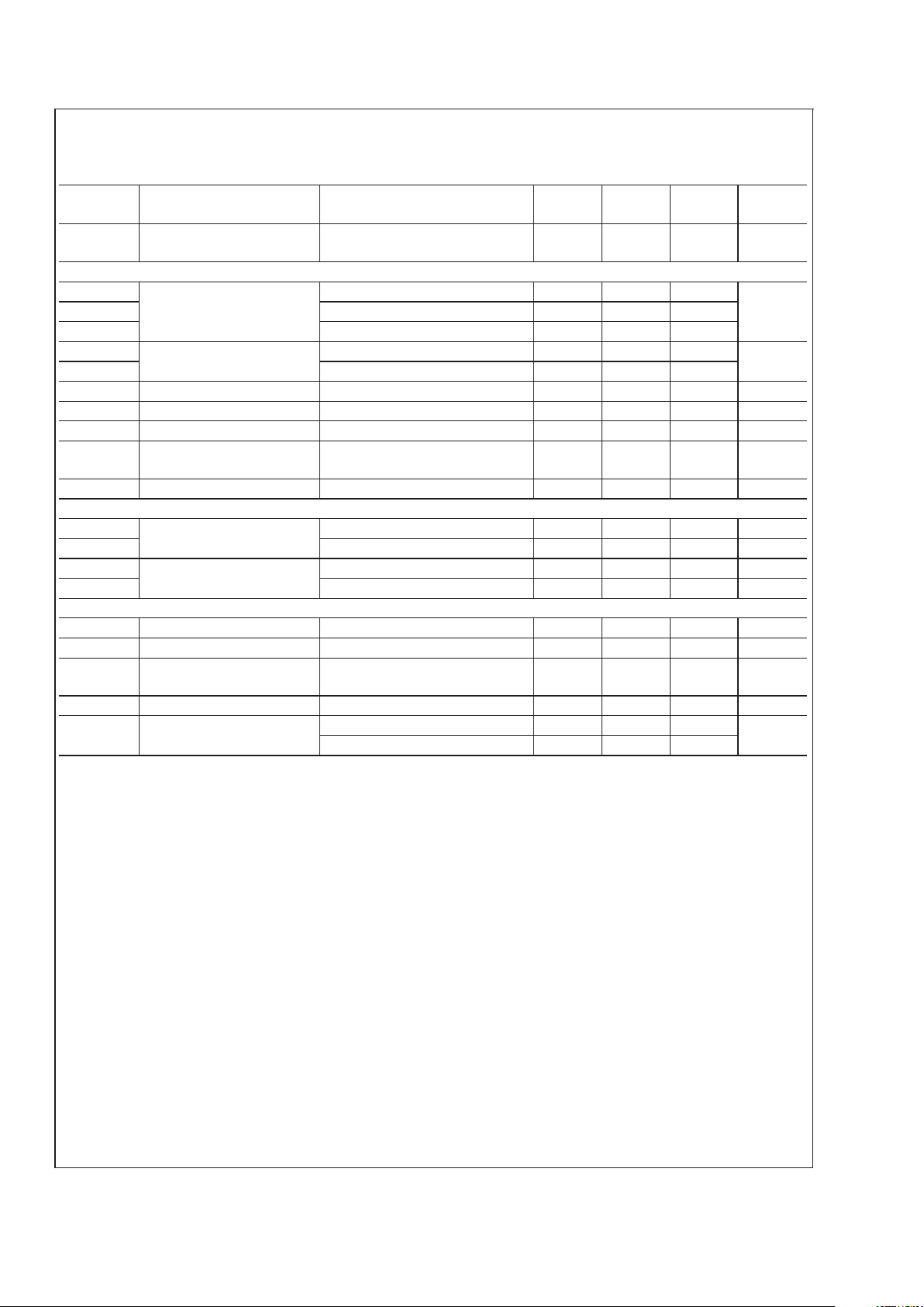
Electrical Characteristics
Specifications with standard typeface are for TJ= 25˚C, and those with boldface apply over full Operating Junction Temperature range. VDD = V5 = 5V, V
SGND=VPGND
= 0V, VIN = 15V, VEN= 3V, R
FADJ
= 22.1K unless otherwise stated. (Note 5)
Symbol Parameter Conditions
Min
(Note 6)
Typical
(Note 7)
Max
(Note 6)
Units
Reference
V
FB_REG
FB Pin Voltage at Regualtion
(either FB Pin)
VDD = 4.5V to 5.5V,
VIN = 5.5V to 28V
591 600 609 mV
VFBLine Regulation VDD = 4.5V to 5.5V,
VIN = 5.5V to 28V
0.5
I
FB
FB Pin Current (sourcing) VFBat regulation 20 100 nA
Chip Supply
I
Q_VIN
VIN Quiescent Current V
FB1=VFB2
= 0.7V 100 200 µA
I
SD_VN
VIN Shutdown Current VEN=0V 0 5 µA
I
Q_VDD
VDD Quiescent Current V
FB1=VFB2
= 0.7V 2.5 4 mA
I
SD_VDD
VDD Shutdown Current VEN=0V 8 15 µA
I
Q_V5
V5 Normal Operating Current V
FB1=VFB2
= 0.7V 0.3 0.5 mA
V
FB1=VFB2
= 0.5V 1 1.5
I
SD_V5
V5 Shutdown Current VEN=0V 0 5 µA
I
Q_BOOT
BOOT Quiescent Current V
FB1=VFB2
= 0.7V 2 5 µA
V
FB1=VFB2
= 0.5V 300 500
I
SD_BOOT
BOOT Shutdown Current VEN=0V 1 5 µA
V
UVLO
VDD UVLO Threshold VDD rising from 0V 3.9 4.2 4.5 V
VDD UVLO Hysteresis VDD = V5 falling from V
UVLO
0.5 0.7 0.9 V
Logic
I
EN
EN Input Current VEN=0to5V 0 µA
V
EN_HI
EN Input Logic High 2 1.8 V
V
EN_LO
EN Input Logic Low 1.3 0.8 V
FPWM Pull-down V
FPWM
=2V 100 200 1000 kΩ
V
FPWM_HI
FPWM Input Logic High 2 1.8 V
V
FPWM_LO
FPWM Input Logic Low 1.3 0.8 V
LM2647
www.national.com5
Page 6
Electrical Characteristics (Continued)
Specifications with standard typeface are for TJ= 25˚C, and those with boldface apply over full Operating Junction Temperature range. VDD = V5 = 5V, V
SGND=VPGND
= 0V, VIN = 15V, VEN= 3V, R
FADJ
= 22.1K unless otherwise stated. (Note 5)
Symbol Parameter Conditions
Min
(Note 6)
Typical
(Note 7)
Max
(Note 6)
Units
Power Good
V
PGOOD_HI
Power Good Upper Threshold
as a Percentage of Internal
Reference
FB voltage rising above V
FB_REG
110 113 116 %
V
PGOOD_LOW
Power Good Lower Threshold
as a Percentage of Internal
Reference
FB voltage falling below V
FB_REG
84 87 90 %
Power Good Hysteresis 7 %
∆t
PG_OK
Power Good Delay From both output voltages “good”
to PGOOD assertion.
10 20 30 µs
∆t
PG_NOK
From the first output voltage “bad”
to PGOOD de-assertion
4 7 10
∆t
SD
From Enable low to PGOOD low 0.03 0.1
PGOOD Saturation Voltage PGOOD de-asserted (Power Not
Good) and sinking 1.5mA
0.12 0.4 V
PGOOD Leakage Current PGOOD = 5V and asserted 0 1 µA
OV and UV Protection
Fault OVP Latch Threshold
as a Percentage of Internal
Reference
FB voltage rising above V
FB_REG
125 130 135 %
Fault UVP Latch Threshold
as a Percentage of Internal
Reference
FB voltage falling below V
FB_REG
65 70 75 %
∆t
FAULT
Fault Delay From Fault detection (any output)
to Fault assertion
7µs
Soft-start
I
SS_CHG
Soft-start Charging Current VSS=1V 8 11 14 µA
R
SS_DCHG
Soft-shutdown Resistance
(SS pin to SGND, either
channel)
V
EN
= 0V, VSS= 1V 1800 Ω
I
SS_DCHG
Soft-start Discharge Current In Current Limit 80 115 160 µA
V
SS_RESET
Soft-start pin reset voltage
(Note 8)
SS charged to 0.5V, EN low to high 100 mV
SS to COMP Offset Voltage V
SS
= 0.5V and 1V, V
FB1=VFB2
=
0V
600 mV
Error Amplifier
GAIN DC Gain 70 dB
Voltage Slew Rate COMP rising 4.45 V/µs
COMP falling 2.25
BW Unity Gain Bandwidth COMP falling 6.5 MHz
COMP Source Current V
FB
<
V
FB_REG
V
COMP
= 0.5V
2 5mA
COMP Sink Current V
FB
>
V
FB_REG
V
COMP
= 0.5V
7 14 mA
Current Limit and Zero-Cross
I
ILIM
I
LIM
Pin Current (sourcing,
either ILIM pin)
V
ILIM1=VILIM2
=0V 46 62 76 µA
I
ILIM
Threshold Voltage -10 0 10 mV
LM2647
www.national.com 6
Page 7
Electrical Characteristics (Continued)
Specifications with standard typeface are for TJ= 25˚C, and those with boldface apply over full Operating Junction Temperature range. VDD = V5 = 5V, V
SGND=VPGND
= 0V, VIN = 15V, VEN= 3V, R
FADJ
= 22.1K unless otherwise stated. (Note 5)
Symbol Parameter Conditions
Min
(Note 6)
Typical
(Note 7)
Max
(Note 6)
Units
V
SW_ZERO
Zero-cross Threshold (SW
Pin)
LDRV goes low -2.2 mV
Osillator
PWM Frequency R
FADJ
= 22.1kΩ 255 300 345 kHz
R
FADJ
= 12.4kΩ 500
R
FADJ
= 30.9kΩ 200
PWM Ramp Peak-to-peak
Amplitude
VIN = 15V 1.6 V
VIN = 24V 2.95
PWM Ramp Valley 0.8 V
Frequency Change with VIN VIN = 5.5V to 24V
±
1%
Frequency Change with VDD VDD = 4.5V to 5.5V
±
2%
Phase Shift Between
Channels
Phase from HDRV1 to HDRV2 165 180 195 deg
FREQ Pin Voltage vs. VIN 0.105 V/V
System
Minimum ON Time V
FPWM
=3V 30 ns
VIN = 5.5V 60 75 %
Maxmimum Duty Cycle VIN = 15V 40 50 %
VIN = 28V, VDD= 4.5V 22 28 %
Gate Drivers
HDRV Source Impedance HDRV Pin Current (sourcing)= 1.2A 7 Ω
HDRV Sink Impedance HDRV Pin Current (sinking) = 1A 2 Ω
LDRV Source Impedance LDRV Pin Current (sourcing) =
1.2A
7 Ω
LDRV Sink Impedance LDRV Pin Current (sinking) = 2A 1 Ω
Cross-conduction protection
delay (deadtime)
HDRV Falling to LDRV Rising 40 ns
LDRV Falling to HDRV Rising 70
Note 1: Absolute maximum ratings indicate limits beyond which damage to the device may occur. Operating Ratings are conditions under which operation of the
device is guaranteed. For guaranteed performance limits and associated test conditions, see the Electrical Characteristics table.
Note 2: PGND1, PGND2 and SGND are all electrically connected together on the PCB.
Note 3: The maximum allowable power dissipation is calculated by using P
Dmax
=(T
JMAX-TA
)/θJA, where T
JMAX
is the maximum junction temperature, TAis the
ambient temperature, and θ
JA
is the junction-to-ambient thermal resistance of the specified package. The 1.0W rating of the TSSOP-28 package for example results
from using 125˚C, 25˚C, and 97˚C/W for T
JMAX,TA
, and θJArespectively. The 2.85W rating of the 28-pin LLP package results from using 125˚C, 25˚C, and 35˚C/W
for T
JMAX,TA
, and θJArespectively. The rated power dissipation should be derated by 10mW/˚C above 25˚C ambient for the TSSOP package and 29mW/˚C above
25˚C ambient for the LLP package. The θ
JA
value above represents the worst-case condition with no heat sinking. Heat sinking will permit more power to be
dissipated at higher ambient temperatures. For detailed information on soldering plastic TSSOP and LLP packages, refer to http://www.national.com/packaging/.
Note 4: ESD is applied by the human body model, which is a 100pF capacitor discharged through a 1.5 kΩ resistor into each pin.
Note 5: R
FADJ
is the frequency adjust resistor between FREQ pin and Ground.
Note 6: All limits are guaranteed at room temperature (standard face type) and at temperature extremes (bold face type). All room temperature limits are 100%
production tested. All limits at temperature extremes are guaranteed via correlation using Statistical Quality Control (SQC) methods. All limits are used to calculate
Average Outgoing Quality Level (AOQL).
Note 7: Typical numbers are at 25˚C and represent the most likely norm.
Note 8: If the LM2647 starts up with a pre-charged soft start capacitor, it will first discharge the capacitor to V
SS_RESET
and then begin the normal Soft-start process.
LM2647
www.national.com7
Page 8
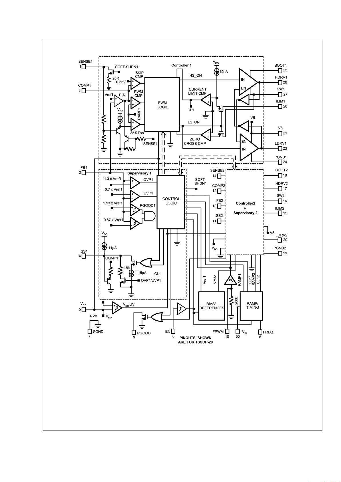
Block Diagram
20056301
LM2647
www.national.com 8
Page 9

Typical Perfromance Characteristics Input Voltage is 15V, 20V, 24V,28V (in order) starting from
uppermost curve to lowermost curve in each of the Efficiency plots below.
Efficiency for 5V/3.3V Outputs Efficiency for 2.5V/3.3V Outputs
20056305 20056306
Efficiency for 1.8V/1.2V Outputs Efficiency for Modulator (Plant) Gain Outputs
20056307
20056308
LM2647
www.national.com9
Page 10

Operation Descriptions
GENERAL
The LM2647 provides two identical synchronously switched
buck regulator channels that operate 180˚ out of phase. A
voltage-mode control topology was selected to provide fixedfrequency PWM regulation at very low duty cycles, in preference to current-mode control, because the latter has inherent limitations in being able to achieve low pulse widths
due to blanking time requirements. Because of a minimum
pulse width of about 30ns for the LM2647, very low duty
cycles (low output, high input) are possible. The main advantage of current-mode control is the fact that the slope of
its ramp (derived from the switch current), automatically
increases with increase in input voltage. This leads to improved line rejection and fast response to line variations. In
typical voltage-mode control, the ramp is derived from the
clock, not from the switch current. But by using the input
voltage together with the clock signal to generate the ramp
as in the LM2647, this advantage of current-mode control
can in fact be completely replicated. The technique is called
line feedforward. In addition, the LM2647 features a userselectable Pulse-skip mode that significantly improves efficiency at light loads by reducing switching losses, and driver
consumption, both of which are proportional to switching
frequency.
INPUT VOLTAGE FEEDFORWARD
The feedforward circuit of the LM2647 adjusts the slope of
the internal PWM ramp in proportion to the regulator input
voltage. See Figure 1 for an illustration of how the duty cycle
changes as a result of the change in the slope of the ramp,
even though the error amplifier output has not had time to
react to the line disturbance. The almost instantaneous duty
cycle correction provided by the feedforward circuit significantly improves line transient rejection.
FORCED-PWM MODE AND PULSE-SKIP MODE
Forced-PWM mode (FPWM) leads to Continuous Conduction Mode (CCM) even at very light loads. It is one of two
user-selectable modes of operation provided by the
LM2647. When FPWM is chosen (FPWM pin high), the
bottom FET will always be turned ON whenever the top FET
is OFF. See Figure 2 for a typical FPWM plot.
20056309
FIGURE 1. Voltage Feedforward
20056310
CH1: HDRV, CH2: LDRV, CH3: SW, CH4: IL(0.2A/div)
Output 1V
@
0.04A, VIN = 10V, FPWM, L = 10µH, f = 300kHz
FIGURE 2. Normal FPWM Mode Operation at Light
Loads
LM2647
www.national.com 10
Page 11

Operation Descriptions (Continued)
In a conventional converter, as the load is decreased to
about 10-30% of maximum load current, DCM (Discontinuous Conduction Mode) occurs. In this condition the inductor
current falls to zero during the OFF-time, and stays there
until the start of the next switching cycle. In this mode, if the
load is decreased further, the duty cycle decreases (pinches
off), and ultimately may decrease to the point where the
required pulse width becomes less than the minimum ONtime achievable by the converter (controller + FETs). Then a
sort of random skipping behavior occurs as the error amplifier struggles to maintain regulation. This is not the most
desirable type of behavior. There are two ways out of this
problem.
One way is to keep the lower FET ON until the start of the
next cycle (as in the LM2647 operated in FPWM mode). This
allows the inductor current to drop to zero and then actually
reverse direction (negative direction through inductor, passing from Drain to Source of lower FET, see Channel 4 in
Figure 2). Now the current can continue to flow continuously
till the end of the switching cycle. This maintains CCM and
so the duty cycle does not start to pinch off as in typical
DCM. Nor does it lead to the undesirable random skipping
described above. Note that the pulse width (duty cycle) for
CCM is virtually constant for any load and therefore does not
usually run into the minimum ON-time restriction. But it can
happen, especially when the application consists of a very
high input voltage, a low output voltage rail, and also the
switching frequency is set high. Let us check the LM2647 to
rule out this remote possibility. For example, with an input of
24V, an output of 1V, the duty cycle is 1/24 = 4.2%. This
leads to a required ON-time of 0.042* 3.3 = 0.14 µs at a
switching frequency of 300kHz (T=3.3 µs). Since 140ns
exceeds the minimum ON-time of 30ns of the LM2647,
normal constant frequency CCM mode of operation is assured in FPWM mode, at virtually any load.
The second way out of the problems of discontinuous mode
is the second operating mode of the LM2647, the Pulse-skip
(SKIP) Mode. In SKIP Mode, a zero-cross detector at the
SW pin turns off the bottom FET when the inductor current
decays to zero (actually at V
SW_ZERO
, see Electrical Characteristics table). This would however still amount to conventional DCM, with its attendant problems at extremely light
loads as described earlier. The LM2647 however avoids the
random skipping behavior described earlier, and replaces it
with a more defined or formal SKIP mode. In conventional
DCM, a converter would try to reduce its duty cycle from the
CCM value as the load decreases, as explained previously.
So it would start with the CCM duty cycle value (at the
CCM-DCM boundary), but as the load decreases, the duty
cycle would try to shrink to zero. However, in the LM2647,
the DCM duty cycle is not allowed to fall below 85% of the
CCM value. So when the theoretically required DCM duty
cycle value falls below what the LM2647 is allowed to deliver
(in this mode), pulse-skipping starts. It will be seen that
several of these excess pulses may be delivered, until the
output capacitors charge up enough to notify the error amplifier and cause its output to reverse. Thereafter several
pulses could be skipped entirely until the output of the error
amplifier again reverses. The SKIP mode therefore leads to
a reduction in the average switching frequency. Switching
losses and FET driver losses, both of which are proportional
to frequency, are significantly reduced at very light loads and
efficiency is boosted. SKIP mode also reduces the circulating currents and energy associated with the FPWM mode.
See Figure 3 for a typical plot of SKIP mode at very light
loads. Note the bunching of several fixed-width pulses followed by skipped pulses. The average frequency can actually fall very low at very light loads. Note however that when
this happens the inductor core is seeing only very mild flux
excursions, and so no significant audible noise is created.
But if EMI is a particularly sensitive issue for the particular
application, the user can simply opt for the slightly less
efficient, though constant frequency FPWM mode.
The SKIP mode is enabled when the FPWM pin is held low
(or left floating). Note that at higher loads, and under steady
state conditions (above CCM-DCM boundary), there will be
absolutely no difference in the behavior of the LM2647 or the
associated converter waveforms based on the voltage applied on the FPWM pin. The differences show up only at light
loads.
Under startup too, since the currents are high until the output
capacitors have charged up, there will be no observable
difference in the shape of the ramp-up of the output rails in
either SKIP mode or FPWM mode. The design has thus
forced the startup waveforms to be identical irrespective of
whether the FPWM mode or the SKIP mode has been
selected.
The designer must realize that even at zero load condition,
there is circulating current when operated in FPWM mode.
This is illustrated in Figure 4. Since duty cycle is the same as
for conventional CCM, fromV=L*∆I/∆t it can be seen that
∆I (or Ipp in Figure 4) must remain constant for any load,
including zero. At zero load, the average current through the
inductor is zero, so the geometric center of the sawtooth
waveform (the center being always equal to load current) is
along the x-axis. At critical conduction (boundary between
conventional CCM and what should have been DCM were it
not in FPWM mode), the load current is equal to Ipp/2. Note
that excessively low values of inductance will produce much
higher current ripple and this will lead to higher circulating
currents and dissipation.
20056311
CH1: HDRV, CH2: LDRV, CH3: SW, CH4: IL(0.2A/div)
Output 1V
@
0.04A, VIN = 10V, SKIP, L = 10µH, f = 300kHz
FIGURE 3. Normal SKIP Mode Operation at Light
Loads
LM2647
www.national.com11
Page 12

Operation Descriptions (Continued)
Note: A common question is: can one change from FPWM to SKIP Mode ‘on
the fly’? That means that the voltage on the FPWM pin would be
changed while the converter is operating normally (with outputs in
regulation). This is generally not recommended. The designer must
realize that doing so would in essence represent a fundamental
change applied to the system. The pulse widths would need to readjust suddenly and in the process momentary imbalances can be
created. For example, there is an observed negative surge current
passing from Drain to Source of the lower FET. It must be kept in mind
that though the LM2647 has current limiting for current passing in the
‘positive’ direction (positive with regards to the inductor, i.e. passing
from Source to Drain of the lower FET), there is no set limit for reverse
currents. The amount of reverse current when the FPWM pin is toggled
‘on the fly’ can be very high. This current is determined by several
factors. One key factor is the output capacitance. Large output capacitances will lead to higher peak reverse currents. The reverse swing will
be worse for lighter loads because of the bigger difference between the
duty cycles/average frequency in the two modes. See Figure 5 for a
plot of what happened in going from SKIP to FPWM mode at 0A load
(worst case). The peak reverse current was as high as 3A, lasting
about 0.1ms. The inductor could also saturate severely at this point if
designed for light loads. In general, if the designer wants to toggle the
FPWM pin while the converter is operating, both the low side FET
rating and the inductor peak current rating must be closely evaluated
under this condition.
SOFT-START
The maximum output voltage of the error amplifier is limited
during start-up by the voltage on the 0.1µF capacitor connected between the SS pin and ground. When the controller
is enabled (by taking EN pin high) the following steps may
occur. First the SS capacitor is discharged (if it has a precharge) by a 1.8 kΩ internal resistor (R
SS_DCHG
, see Electrical Characteristics). This ensures that reset is obtained.
Note that reset is said to occur only when the voltage on both
the SS pins falls below 100mV (V
SS_RESET
, see Electrical
Characteristics table). Then a charging current source
I
SS_CHG
of 11µA is applied at this pin to bring up the voltage
of the Soft-start capacitor voltage gradually. This causes the
(maximum allowable) duty cycle to increase slowly, thereby
limiting the charging current into the output capacitor and
also ensuring that the inductor does not saturate. The Softstart capacitor will eventually charge up close to the 5V input
rail. When EN is pulled low the Soft-start capacitor is discharged by the same 1.8 kΩ internal resistor and the controller is shutdown. Now the sequence is allowed to repeat
the next time EN is taken high.
The above Soft-start sequence is actually initiated not only
whenever EN is taken high, but also under a normal
power-up or during recovery from a fault condition (more on
this later).
As mentioned in the section ‘Forced-PWM Mode and Pulseskip Mode’ under startup, since the currents are high until the
output capacitors have charged up, there will be no observable difference in the shape of the ramp-up of the output rails
in either SKIP mode or FPWM mode. The design has thus
forced the startup waveforms to be identical irrespective of
whether the FPWM mode or the SKIP mode has been
selected.
SHUTDOWN/SOFT-SHUTDOWN
When the EN pin is driven low, the LM2647 initiates shutdown by turning OFF both upper and lower FETs completely
(this occurs irrespective of FPWM or SKIP modes). See
Figure 6 for a typical shutdown plot and note that the LDRV
20056312
FIGURE 4. Inductor Current in FPWM Mode
20056313
CH1: PGOOD, CH2: Vo, CH3: LDRV, CH4: IL(1A/div)
Output 1V
@
0A, VIN = 10V, L = 10µH, f = 300kHz
FIGURE 5. SKIP to FPWM ’On The Fly’
LM2647
www.national.com 12
Page 13

Operation Descriptions (Continued)
goes to zero (and stays there). Though not displayed, Power
Good also goes low within less than 100ns of the EN pin
going low (∆t
SD
, see Electrical Characteristics table). Therefore in this case, the controller is NOT waiting for the output
to actually fall out of the Power Good window before it
signals Power Not Good. Note that since there is a constant
current 2A load applied at the output, the stored charge on
the output capacitor continues to be discharged into the
load. From ∆V/∆t=i/C=2A/330µF it can be seen that the
output voltage (say 1V) will fall to zero in about 165µs, as will
be observed.
But if the load is very close to zero, the only means for the
output capacitor to discharge is through the resistive divider
on the feedback pin (if any) and any internal bleeder resistor
present. In fact there is such an internal bleeder resistor in
the LM2647 and it performs Soft-shutdown by discharging
the output capacitors gradually. Its value is about 20Ω and it
is internally connected between the SENSE pin and ground
whenever the EN pin is taken low. Note that this will be
perceivable only when the external load is small, and provided a normal shutdown is being carried out. Normal shutdown as being defined here calls for the Enable pin to be the
cause of the outputs being disabled. In a shutdown provoked
by a fault, the situation is very different as will be explained
later.
POWER GOOD/NOT GOOD SIGNALING
PGOOD is an open-Drain output pin with an external pull-up
resistor connected to 5V. It goes high (non-conducting) when
both the outputs are within the regulation band as determined by the Power Good window detector stage on the
feedback pin (see Block Diagram). PGOOD goes low (conducting) when either of the two outputs falls out of this
window. This signal is referred to as Power Not Good here.
A glitch filter of 7µs filters out noise, and helps prevent
spurious PGOOD responses. So Power Not Good is not
asserted until 7µs after either of the two outputs have fallen
out of the Power Good window (see ∆t
PG_NOK
in Electrical
Characteristics table). With the feedback pin voltage rising
towards regulation value, there is a 20µs delay between both
the outputs being in regulation and the signaling of Power
Good (see ∆t
PG_OK
in Electrical Characteristics table).
Power Not Good is signaled within 100ns of the Enable pin
being pulled low (see ∆t
SD
in Electrical Characteristics
table), irrespective of the fact that the outputs could still be in
regulation. The Soft-start capacitor is also then discharged
as explained earlier.
VIN POWER-OFF
The LM2647 has an internal comparator that also looks at
VIN. If VIN falls to about 4.5V (roughly), switching ceases.
The response is slightly different under FPWM or SKIP
modes, but the final result is the same. In both cases ultimately, LDRV is latched high and so the output capacitors
are discharged through the lower FETs. Power Not Good
has meanwhile already been signaled and a fault condition is
asserted shortly thereafter.
In Figure 7 and Figure 8 the situation where the connection
to the input DC power source is abruptly removed is shown
for two cases.
In the first case (FPWM mode, Figure 7), LDRV goes high
immediately, as soon as VIN falls to about 4.5V. For the
second case (SKIP mode, Figure 8), the output starts to
discharge into the load resistor. Then Power Not Good is
signaled. Finally, when the output falls below the Undervoltage threshold a fault condition is asserted. This is accompanied by LDRV latching high. The output then suddenly
collapses just as it does for FPWM mode. Note that once
VIN reaches 4.5V, it does not fall quickly thereafter. The
reason is that there is no applied external voltage dragging it
low (in our case as it is described), nor is there any significant consumption from the VIN rail since the converter has
stopped switching.
20056314
CH1: LDRV, CH2: Vo, CH3: SW, CH4: IL(1A/div)
Output 1V
@
2A, VIN = 10V, FPWM/SKIP, L = 10µH, f = 300kHz, C
OUT
=
330µF
FIGURE 6. Shutdown
20056315
CH1: PGOOD, CH2: VIN, CH3: LDRV, CH4: Vo
Output 1V
@
0.02A, VIN = 9.75V, FPWM, L = 10µH, f = 300kHz, C
OUT
=
660µF
FIGURE 7. VIN Removal in FPWM Mode
LM2647
www.national.com13
Page 14

Operation Descriptions (Continued)
The recovery procedure from a VIN Power-off is the same as
for any fault condition.
VDD POWER-OFF (UVLO)
Whenever VDD starts to fall, and drops below about 4V,
LDRV goes high immediately, ‘Power Not Good’ is signaled
and in effect a fault condition (in this case an Under-voltage
lockout) is asserted. Recovery from a fault is discussed next.
FAULT AND RECOVERY
If any output falls outside the Power Good window, the
response is a ‘Power Not Good’ signal. The FET drive signals are not affected. But under a fault condition assertion,
LDRV goes high immediately turning the low side FETs ON
and discharging the output capacitors. Note that the current
will then invariably slew momentarily negative (passing from
Drain to Source of lower FETs), before it settles down to
zero.
A fault will be detected when either output falls below the
Under-voltage threshold, or rises above the Over-voltage
threshold. From its detection to assertion, there is a 7µs
delay to help prevent spurious responses.
A fault condition is also asserted during a loss of the VIN rail
or the VDD rail, though not if shutdown is achieved by use of
the Enable pin.
To recover from a fault, either of the following options is
available:
a) Enable pin is toggled: i.e. taken low (below 0.8V), then
high again (2V to 5V). This must be done with VDD between
4.5V to 5V and VIN within normal range (5.5V to 28V).
b) VDD is brought below 1.0V and then brought back up
between 4.5V to 5V. This must be done with the Enable pin
held high (2V to 5V) and VIN within normal range (5.5V to
28V).
Recovery will initiate a Soft-start sequence (see description
under section ‘Soft-start’ above).
CURRENT LIMIT AND PROTECTION
Output current limiting is achieved by sensing the negative
Vds drop across the low side FET when the FET is turned
on. The Current Limit Comparator (see Block Diagram)
monitors the voltage at the ILIM pin with 62µA (typical value)
of current being sourced from the pin. The 62µA source flows
through an external resistor connected between ILIM and
the Drain of the lower FET. The voltage drop across the ILIM
resistor is compared with the drop across the lower FET and
the current limit comparator trips when the two are of the
same magnitude. This determines the threshold of current
limiting. For example, if excessive inductor current causes
the voltage across the lower FET to exceed the voltage drop
across the ILIM resistor, the ILIM pin will go negative (with
respect to ground) and trip the comparator. The comparator
then sets a latch which prevents the top FET from turning
ON during the next PWM clock cycle. The top FET will
resume switching only if the current limit comparator was not
tripped in the previous switching cycle.
The Soft-start capacitor at the SS pin is discharged with a
115µA current source when an overcurrent event is in
progress. Therefore if the overcurrent condition does not last
long enough to cause a fault assertion, the Soft-start capacitor will charge back up (by I
SS_CHG
, see Electrical Characteristics table), without any user intervention. The purpose of
discharging the Soft-start capacitor during an overcurrent
event is to eventually allow the voltage on the SS pin to fall
low enough to cause additional duty cycle limiting (over and
above the protection provided by the adaptive duty cycle
clamp). Note that once the duty cycle starts pinching-off as a
result of the progressive reduction in SS pin voltage, the
output voltage will certainly start collapsing (if it hasn’t done
so already), and this will hasten a fault condition assertion
(an Under-voltage in this case). Thereafter, a normal faultrecovery sequence will have to be initiated to cause the
outputs to return to regulation.
There is a race condition in effect, between the current limit
being reached and a fault being asserted (Under-voltage). It
could happen that if the load current was very low before the
sudden overload was applied, a fault condition could be
asserted even before the current limit has been reached.
See the differences between Figure 9 and Figure 10 to see
the possibilities. Also see ‘Application Information’ for a
deeper understanding of current limiting discussed at a
quantitative level.
20056316
CH1: PGOOD, CH2: VIN, CH3: LDRV, CH4: Vo
Output 1V
@
0.02A, VIN = 9.75V, SKIP, L = 10µH, f = 300kHz, C
OUT
=
660µF
FIGURE 8. VIN Removal in SKIP Mode
LM2647
www.national.com 14
Page 15

Operation Descriptions (Continued)
20056317
20056360
CH1: PGOOD, CH2: Vo, CH3: ILIM Pin, CH4: IL(1A/div)
Output 1V, 0.04A to Overload, VIN = 10V, FPWM, L = 10µH, f = 300kHz,
RLIM = 1k
FIGURE 9. Response to Severe Overload (Type A: fault
threshold first)
20056318
20056361
CH1: LDRV, CH2: PGOOD, CH3: ILIM Pin, CH4: IL(5A/div)
Output 1V, 2A to Overload, VIN = 10V, L = 10µH, f = 300kHz, RLIM = 2k
FIGURE 10. Response to Severe Overload (Type B:
current limit threshold first)
LM2647
www.national.com15
Page 16

Application Information
CURRENT LIMIT RESISTOR
The timing scheme implemented in the LM2647 makes it
possible for the IC to continue monitoring an overcurrent
condition and to respond appropriately every cycle. This is
explained as follows.
Consider the LM2647 working under normal conditions, just
before an overload occurs. After the end of a given ON-pulse
(say ‘ton1’), the LM2647 starts sampling the current in the
low-side FET. This is the OFF-duration called ‘toff1’ in this
analysis. Therefore, if an overcurrent condition is detected
during this OFF-duration ‘toff1’, the controller will decide to
omit the next ON-pulse (which would have occurred during
the duration ‘ton2’). This is done by setting an internal ‘overcurrent latch’ which will keep HDRV low. The LDRV will now
not only stay high during the present OFF-duration (‘toff1’)
but during the duration of the next (omitted) ON-pulse
(‘ton2’), and then as expected also during the succeeding
OFF-duration (‘toff2’). But the ‘overcurrent latch’ is reset at
the very start of the next OFF-duration ‘toff2’. Therefore if the
overcurrent condition persists, it can be recognized during
‘toff2’ and a decision to skip the next ON-pulse (duration
‘ton3’) can be taken. Finally, several ON-pulses may get
skipped until the current in the lower FET falls below the
current limit threshold.
Note that about 150ns after LDRV first goes high (start of
low-side conduction), the current monitoring starts. Therefore the peak current seen by the current limit detector is
almost the same as the peak inductor current.
To set the value of the current limiting resistor (‘RLIM’, between ILIM pin and SW pin), the function of the ILIM pin must
be understood. Refer to Figure 11 to see how the voltage on
the ILIM pin changes as current ramps up. For this analysis
note that the worst case has been taken here by using the
minimum possible value of the current sourced (I
ILIM
, see
Electrical Characteristics table). Also, the maximum value of
the ‘hot’ Rds of the lower FET should be used. For example
if the chosen low-side FET is the Si4420DY from Vishay, the
typical Rds at room temperature is 10mΩ (but this is not the
value to be used here). The MAX is the relevant number
which is 13mΩ. Now applying the thumbrule that at 100˚C
the Rds goes up typically 1.4 times (for 30V FETs), the Rds
to be used in the actual current limit calculation is
1.4*13mΩ=18.2mΩ. Therefore using 46µA for I
ILIM
(see
Electrical Characteristics table) and Rds = 18.2mΩ here will
provide the lowest value of current limit (considering tolerances and temperature for a chosen RLIM resistor). This
current limit must obviously be higher than the actual peak
current in the converter under normal operation to ensure
that full rated power can be delivered under all conditions by
the converter without ‘inadvertently’ hitting the worst case
(lowest value) set current limit.
The detector sets the overcurrent latch as soon the voltage
on the ILIM pin crosses below zero. Therefore the basic
design equation for calculating RLIM is:
∆V = v (see Figure 11)
At the point where current limiting occurs (peak inductor
current becomes equal to current limit) the resistor for setting
the current limit can be calculated.
But what (peak) current limit value should actually be set?
This depends on two factors:
a) There is a natural steady state peak current in the inductor
with the converter delivering maximum rated load. This
should be calculated at VIN
MAX
(the maximum of the input
voltage range):
b) Over and above this steady state value we need to
provide an ‘overload margin’. This margin will depend on the
step loads likely to be seen in the application and the response expected.
The equation for calculating the steady state peak current is:
where ‘r’ is the current ripple ratio (refer to Application Note
AN-1197 at http://power.national.com for a detailed understanding of how ‘r’ affects all the power components). ‘r’ is
given by:
where L is in µH, f is in Hz.
Example: Let VIN range from 5.5V to 28V, Vo=5V, Io=3A,
L=10µH, f=300kHz. What is the peak current under normal
operation?
Only the highest input voltage must be used for any peak
current calculation. At VIN
MAX
the duty cycle is D=Vo/Vin=5/
28=18%. So
Note: In general, as discussed in AN-1197, the optimum value of ‘r’ is
between 0.3 to 0.5. Large inductances (higher than ‘optimum’) may be
20056319
FIGURE 11. Understanding Current Sensing
LM2647
www.national.com 16
Page 17

Application Information (Continued)
selected if the output voltage ripple needs to be decreased but it is not
desirable to achieve this by adding more (expensive?) output specialty
caps.
The peak current under normal operation is
Conclusions: In this example the peak inductor current
under normal operation is 3.7A. Usually it is necessary only
to set the current limit about 20% higher than the peak value.
This ‘overload margin’ helps greatly in handling sudden load
changes. A 20% margin would have required the current limit
to be set at 3.7*120%=4.44A (for a steady state peak of
3.7A). Therefore RLIM would need to be
A standard resistor value of 1.78k can be chosen in the
example. However, a larger overload margin than the chosen 20% (say 40%) is recommended for obtaining good
dynamic response if the load could suddenly change from
extremely low values (zero to a few mA) right up to maximum
load current. In this case, it would require
I
CLIM
=3.7*140%=5.2A, requiring RLIM to be 18.2m*5.2/
46µ=2.05k (available as a standard value).
Note that excessively high current limits (large RLIM values)
will generate severe stresses in the FETs during abnormal
load condition (like a shorted output for example). These
peak currents will be even higher if the inductor saturates
sharply. The designer must evaluate the actual application
for the expected and actual step loads so as to select RLIM
more optimally. Then it should be decided how much overload margin is really required, and RLIM selected accordingly. The equations to do this are provided in this section,
but the judgement must remain with the designer, as it
depends on the specific application on hand.
Repeating the calculation for a 10µH inductor for a 3.3V/3A
rated output, and any low side equivalent FET (with the
same Rds as Si4420DY) we get the following requirement:
For 20% overload margin, select current limit resistor to be
1.69k
For 40% overload margin, select current limit resistor to be
1.96k
Note that if the lower FET Rds is different from the one used
in the example above, the current limit resistor RLIM must be
recalculated according the new Rds.
For the evaluation board the selected FET was a dual pack
Si4828DY. Its worst case hot Rds is 24.5mΩ. Setting current
limit as 5.5A, the estimated current limit resistor is 5.5 x 24.5
/ 46 = 2.93kΩ. A standard value of 2.94kΩ was chosen for
the Bill of Materials.
INDUCTOR and OUTPUT CAPACITOR
The designer is again referred to AN-1197 for the equations
required here. In general, ‘r’ is the key parameter and once
that is chosen, the inductance can be calculated. The design
table in the referenced Application Note uses V
D
as the drop
across the diode in an asynchronous configuration. Also,
V
SW
is the drop across the Switch (upper FET). In the case
of the LM2647 a reasonable approximation is to set V
D
=
V
SW
= 0 in the design table available in AN-1197. Then the
table can be used easily for selection of the inductor and
output capacitor. A step by step example is also provided for
a general buck regulator in the Application Note AN-1207 at
http://power.national.com.
Only in the case of the input capacitor, the situation may be
different as is explained next.
INPUT CAPACITOR
In a typical single-channel buck regulator, the input capacitor
provides most of the pulsed current waveform demanded by
the Switch. However the DC (average) value of the current
through a capacitor in steady state must be zero. Otherwise,
the capacitor would start accumulating charge every cycle,
and that would clearly not represent a ‘steady state’ by
definition.
Now for the LM2647, there are two ways of calculating and
meeting the input capacitance requirement. One way is to
use separate input capacitors for each channel (as in the
Evaluation board). The other possibility is to combine them
into a single component. There are advantages and disadvantages to each approach.
By keeping separate input capacitors the possibility of interaction between the two channels is reduced, and the layout
is a little more forgiving. But two components would require
more board space and could also add to the cost. Though in
general, there could also be a situation where the cost of a
single component is equal to (or even exceeds) the combined cost of two separate capacitors. The reason cost can
be surely reduced when using one input capacitor in the
LM2647 is because the two channels run 180˚ out of phase
(interleaved switching). It can be shown that this dramatically
reduces the ripple current requirement at the input. See
Figure 12 for typical waveforms to understand how this
happens. Remember that ‘frequency’ does not (directly) enter into any computations of RMS values, so the use of
interleaved switching is clearly going to produce a lower
RMS value as can be guessed by eyeballing the waveforms
shown in Figure 12.
20056327
FIGURE 12. Switch and Input Capacitor Currents
LM2647
www.national.com17
Page 18

Application Information (Continued)
The case of a single input capacitor supplying two channels
running out of phase is now discussed in detail and it shows
how to formally calculate the input RMS current capability
required. The example represents a very general case in
terms of the output voltages simply to highlight the various
possible applications of the LM2647 other than its primary
intended application. One of the most important questions to
answer here is: what input voltage really gives the worst
possible (highest) input RMS current? This information is
required to size the capacitor correctly.
Example: Consider two channels running at 5V
@
3A and
3.3V
@
3A. What is the worst case input capacitor RMS cur-
rent if the input varies from 10V to 28V?
Step1: Call the output with the higher voltage as Vo1 and the
other as Vo2. Then find the ratio ‘y’ as shown below
y is clearly going to be equal to or less than 1 by definition
(since Vo2 ≤ Vo1). This step is required for using the equation presented in the next step.
Step2: The equation for the input current has been derived
and it reveals that the worst-case occurs when the duty cycle
of the first channel is
where ‘y’ has been defined in Step 1. So
Therefore the appropriate input voltage to calculate the
worst case RMS input current is
Step3: Calculate the duty cycle of the other channel when
this happens
Step4: Calculate input capacitor RMS current by using the
known equation
I
IN
2
= (Io1
2
•
D1) + (Io2
2
•
D2) - [Iol•D1+Io2•D2]
2
I
IN
2
=(3
2
•
0.3) + (3
2
•
0.2) - [(3•0.3) + (3•0.2)]
2
Solving
I
IN
= 1.5A
Step5: But what is really the worst case??
It may have simply concluded at this point that "the rating of
the input capacitor must be greater or equal than 1.5A,
otherwise the life/reliability of the capacitor may be affected
severely etc.". And that is true but only under the single-point
load conditions used for the calculation. It will now be seen
that the worst case may still have gone unrecognized! What
if maximum load currents are not being drawn simultaneously as was assumed in our example? It can be shown
that the capacitor could actually see higher currents than
calculated in Step 4.
Suppose one channel was completely unloaded. So in effect
there is only a single output of 5V
@
3A. The equation for the
RMS current through the input capacitor is then
The function D(1-D) has a maxima at D = 0.5. This would
correspond to an input voltage of 5V/0.5 = 10V. And the input
capacitor current at this worst case input voltage would be
It is just a coincidence in this application that in both cases
(above and at the end of Step 4) we have calculated the
same RMS current rating for the capacitor. In general, Step
4 can certainly yield smaller values than those for a single
channel, and this may mislead us into an improper selection
of the input capacitor. It must be remembered that Step 4 is
not necessarily the worst case. We must always take the
higher of the two values so calculated.
Incidentally, the above method for a single channel is also
the method to be used to calculate the capacitor rating when
the LM2647 is formally used for single channel operation, or
if both channels are being used but separate input capacitors are being allocated for each channel.
In all cases the input capacitors must be positioned physically close to their respective stages. But if separate input
capacitors are being used for each channel, the input traces
to the two inputs must be long and thin so as to introduce a
measure of high frquency decoupling between the now
separated stages.
The designer may ask, what is the use of interleaved switching if the result of the interleaved calculation in Step 4 may
not even be used in our particular example? Interleaved
switching certainly reduces cost because if the calculation
had been carried out for two non-interleaved channels
(switching in phase), both delivering maximum load, the
capacitor RMS current would have been much higher.
Note that the equations used in the above sections apply
only if the duty cycles of both channels are less than or equal
to 50% (and there is therefore no overlap in the current
waveforms). The equations for overlapping waveforms are
out of scope here.
MOSFETs
The selection of the MOSFETS should be done carefully to
maximize both efficiency and reliability together. There is a
different set of criteria for selecting the upper FET and lower
FET. It will also be seen that using very fast FETs without
deliberate thought, may seem to improve efficiency dramatically on one prototype board but can impair efficiency on
another apparently ‘identical’ board, specially at light loads.
Therefore, the quest for improved efficiency must be
weighed against the possible penalty for doing this without
deeper understanding of the nuances of synchronous
switching buck stages in general. The criteria for selection
are briefly:
a) The upper FET is chosen basically for high switching
speed because in a typical synchronous buck regulator only
LM2647
www.national.com 18
Page 19

Application Information (Continued)
the upper FET sees the V-I crossover losses (at turn-ON and
at turn-OFF). So to maximize efficiency, high switching
speed is certainly needed in this position. This FET position
has typically very low conduction losses, especially in a
power supply for mobile applications since the duty cycle is
very low. So the Rds is not of much direct concern here. A
possible choice of FET for the upper position on the Evaluation board is the Si4800DY from Vishay (www.vishay.com).
The threshold voltage (MIN value) of a FET in this position
can be 0.8V but 1.0V is preferable. Note however that if the
upper FET is chosen so that it switches too fast, it can induce
a shoot-through (called a CdV/dt turn-on of the lower FET)
whenever the upper FET turns on hard. Therefore, Q
G
of the
upper FET should not be much less than 8nC.
b) The lower FET sees no V-I crossover loss in principle
(under most situations). Also, since it can conduct for the
complete OFF-time, its Rds becomes important, especially
at low duty cycles. This FET is therefore chosen basically for
its low Rds, not necessarily speed. A high C
OSS
for this FET
position also helps, by reducing the possibility of CdV/dt
turn-on of this FET, by snubbing the rising edge of voltage
applied on the lower FET when the upper FET turns ON.
Note that too high a C
OSS
value will degrade efficiency. An
acceptable compromise figure for C
OSS
of the lower FET is
350-800pF. A possible choice of FET for this position is the
Si4420DY from Vishay. The C
OSS
of this FET is about 700pF
at 24V. The threshold voltage for the lower FET position
must also be 1V or slightly higher. Too high a threshold will
prevent the FET from turning ON fully, and too low a value
will increase the likelihood of a CdV/dt turn-on. Also note that
one of the factors which can provoke a spurious turn-on is
layout. In particular, the source lead/trace of a given FET
must be kept short and the copper area around it large to
reduce inductive spikes during transitions. Gate trace
lengths must also be kept short.
Note that the threshold voltage of a FET should have both
MIN and MAX limits as per its datasheet. Since it is important
that the FET turn on fully, ensure that the threshold voltage is
guaranteed to be below 3V. Contact the FET vendor if necessary. If the threshold voltage is too high, foldback might
result upon hitiing current limit. This will result in failure of the
output to recover after an overload condition.
EFFICIENCY ESTIMATE
A sample calculation follows based on the low cost FETs
used on the Evaluation Board. The device is the Si4828DY
from Vishay.
The extension ’_u’ stands for the upper FET (half
Si4828DY), and ’_l’ for the lower FET (half Si4828DY). The
general equation is first stated and then the numerical result
is quoted (in bold). The case is for V
IN
=20V, Vo=5V, Io=3A.
The frequency is set to 300kHz. Note that efficiency estimates are usually based on typical values. Therefore, in the
calculations below the typical value of the gate charge Q
G
is
used. For the Si4828DY the typical values as declared in its
datasheet (available at the time of writing this section) are
Q
G
(upper) = 8nC, QG(lower) = 23nC, Rds(upper) = 24mΩ,
Rds(lower) = 14.5mΩ
FET Conduction losses
Pcond_u = 54mW
Pcond_l = 98mW
FET Switching Losses
The transition times must first be determined. A simplified
equation available in related literature is:
This equation is applied to our case by setting the pulse
amplitude Vp to 5V. Suppose the output impedances of the
IC are (in ohms):
Rpon_u = 7
Rpoff_u = 2
Rpon_l = 7
Rpoff_l = 1
Therefore transition times are
ton_u = 51.5ns
toff_u = 15ns
ton_l = 148ns
toff_l = 21ns
The switching loss for any V-I crossover when driving an
inductive load is in general
Pcross = 1/2xVxIxtcross x freq
LM2647
www.national.com19
Page 20

Application Information (Continued)
The V-I crossover losses (exist only in upper FET) are:
Pswon_u = 1/2
•
VIN•Io•f•ton_u
Pswon_u = 464mW
Pswoff_u = 1/2
•
VIN•Io•f•toff_u
Pswoff_u = 232mW
There is another loss term associated with charging C
OSS
every cycle, then dumping it into the FET before the next
charge cycle. This applies to both upper and lower FETs.
Pcoss_u = 1/2
•
C
OSS_u
•
VIN
2
•
f
Pcoss_l = 1/2
•
C
OSS_l
•
VIN
2
•
f
From the datasheets of the chosen FETs, ’Coss’ are respectively about:
C
OSS_u
= 250pF
C
OSS_l
= 500pF
So
Pcoss_u = 15mW
Pcoss_I = 30mW
Summing up,
Psw_u = 464+132+15=611mW
Psw_I = 30mW
Controller Losses
In addition to the losses in the FETs, there is another loss
term associated with the switching, and this is dissipated in
the controller. The LM2647 has to pump in current pulses at
each transition to turn-ON or turn-OFF the FETs. Several
simplified or more complicated equations exist for calculating this, but this is most easily deduced by simply turning to
the measured consumption (see Electrical Characteristics
table). The current into the V5 pin is I
Q_V5
and reflects the
driver consumption. This can be as high as 1.5mA (measured at 300kHz). Let us also include the current into the
control sections (VDD pin), which can be as high as 4mA.
The total controller consumption is therefore
P
IC
=(I
Q_V5+IQ_VDD
)x5
P
IC
= 28mW
Inductor Losses
The DC resistance (‘DCR’) of the chosen inductor is typically
is 26mΩ. The DC loss is therefore DCR*Io
2
. The core losses
typically add 10% more to this. Therefore our estimate of
total inductor loss is
Pind=1.1 x (DCR x Io
2
)
Pind = 257mW
Capacitor Losses
The output capacitor of a typical buck regulator has very low
ripple current going through it. So its loss term can be
ignored. The input capacitor however provides the sharp
pulses of current for the Switch, and therefore the RMS
current through it can be fairly high. But the dissipation can
still be negligible if the ESR is very low. This is the situation
if the input capacitors are monolithic ceramic capacitors as in
the Evaluation board (if Tantalum or Aluminum electrolytic
capacitors are used at the input, their dissipation must be
accounted for here). The final efficiency/loss terms are provided in Table 1.
20056323
FIGURE 13. Crossover (turn-on or turn-off)
LM2647
www.national.com 20
Page 21

Application Information (Continued)
TABLE 1. Losses and Efficiency
Upper Lower
Pcond (mW) 54 98
Psw (mW) 611 30
PFET (mW) 665 128
P
IC
(mW) 28
Pind (mW) 257
Ptotal (mW) 1078
Pout (=VoxIo) (mW) 15000
93%
Vo=5V, Io=3A,Vin=20V, f=300kHz, DCR=26mΩ, Si4828DY.
Typical efficiency curves for different input voltages are available under Typical Performance Characteristics.
LAYOUT GUIDELINES
For a deeper understanding of Buck converters and the
‘critical traces’ please see Application NoteAN-1229 at http://
power.national.com.
Figure 14 is based on such an understanding of the critical
sections and also the pin functions of the LM2647. Refer to
the Typical Applications circuit and the LM2647 TSSOP pinouts to understand the layout suggestions more thoroughly.
The components shown in Figure 14 are most critical and
must be placed close to the device and connected onto a
ground island on the component side. Several vias can then
connect to the ground plane at the locations indicated. The
FETs are positioned close to the controller and are also very
close to each other to minimize inductances.
After the critical components are placed, the resistor to the
frequency adjust pin (R19) must also be placed close to the
IC connecting to SGND. This will reduce noise pickup and
jitter.
The feedback trace can also pick up noise and it must be
routed away from sources of noise/EMI, particularly the
FETs and inductors.
Enough copper area must be left around the FETs for thermal dissipation. More details on this are also provided in
AN-1229.
Note that the current limit detector circuit compares the
voltage on the ILIM pin with respect to the PGND pin.
Therefore, if the power ground is noisy it can lead to erroneous triggering of the current limit detector. This will manifest
itself as an inability to meet the load requirement despite
oversizing the current limit resistor. It can also lead to failure
of the output to recover after encountering an overload condition. Therefore, it is strongly recommended that a solid
ground plane be created as the first internal plane right
below the component side.Several vias should be generously placed to connect the ground nodes of the component
layer to this ground plane.
SETTING OUTPUT VOLTAGE
From the Typical Application circuit on Page 1, it can be seen
that R15 and R16 are used to set V
O2
whereas R21 and R22
set V
O1
. For either channel, calling the upper resistor (con-
nected to one end of the droop resistor) R
U
and the lower
resistor (connected to ground) R
L
the following equation is
applicable.
Therefore from the Bill of Material:
For channel #1 (V
O1
=5V),
R
U
= R21 = 43.2k
R
L
= R22 = 5.9k
For channel #1 (V
O2
= 3.3V),
R
U
= R15 = 43.2k
R
L
= R16 = 9.53k
So
This is as per the requirement of the primary end-application.
Other output voltage values are possible by adjusting the
resistor ratios (but note that there are maximum duty cycle
constraints as stated in Electrical Characteristics table)
which will limit the range of output voltages achievable. Note
that the upper resistor is involved in fixing the gain of the
error amplifier, and therefore its value has been set to an
‘optimum’ value of 43.2k for both channels. This value helps
in achieving good step response and ensuring stability.
Therefore, in general, only the lower resistor should be
adjusted. However the more experienced designer can judiciously use the open-loop gain information provided in the
next section, to change both upper and lower resistor values
if required.
20056343
FIGURE 14. Critical Component placement (TSSOP)
LM2647
www.national.com21
Page 22

Application Information (Continued)
MODULATOR GAIN/COMPENSATION
The modulator gain is plotted out for various typical values of
components in Typical Performance characteristics. The
curves were based on the following information. The plant/
modulator gain ‘G’ is:
where Ro is the load resistance,s=jω, and
A1 = LC*(Ro + esr)
A2={L+R
P
C(Ro + esr) + Ro*esr*C}
A3=R
o+RP
Here esr is the Equivalent Series Resistance of the output
capacitor, Ro is the load resistance, C is the output capacitance, L is the inductance, and R
P
is the resistance of the
power stage (Rds+ DCR etc, typically about 40mΩ). V
RAMP
is about 1.6V for the LM2647. The unity gain bandwidth of
the error amplifier is taken as 6.5MHz.
Let us assume Type 3 compensation Figure 15.
The design procedure is summarized in Table 2.
TABLE 2. Summary of Compensation Design Procedure
fp1 fz1 fz2 fp2 fp3
Type 3 (C1) R2, C2 R1sR3, C3 R2, C1sC2 C3, R3
Resonant frequency f =1⁄2πRC, ’s’ stands for series combination.
TABLE 3.
C1 C2 C3 R2 R3
A is a factor to shift entire Gain up or down to acheive good crossover frequency and gain. Typically set A = 0.2 here.
TABLE 4.
fp1 fz1 fz2 fp2 fp3
(0) fdp fdb fesr fsw/2
Resonant frequency f =1⁄2πRC, ’s’ stands for series combination.
A short explanation on Table 2 follows. For example from the
table it can be seen that the second zero is created by the
series combination of R1 and R3 resonating with C3. So the
frequency of this zero is at 1/2π(R1+R3)*C3. The solution for
calculating the component values follows. For example, C3
is set as
But where should the designer position the poles and zeroes
of the error amplifier, taking into account the modulator gain,
so as to achieve good closed loop characteristics? A typical
scenario is also provided in Table 4. For example it suggests
that both the first and second zeroes should be positioned at
the point where double pole (fdb) of the output LC filter is.
This double pole is known to occur at about.
Similarly, the esr zero occurs at fesr which is at
where C is the output capacitance
Thus all the components can be calculated easily
EVALUATION BOARD DETAILS
The Bill of Materials is now provided for the LM2647 Evaluation board. The schematic is the Typical Application circuit.
See Layout Guidelines for more guidance on preferred layout practices and also refer to Application Note AN-1229.
Note that a dual FET pack has been chosen for the Evaluation Board.
The Evaluation board has two outputs V
O1
= 5V and VO2=
3.3V as discussed under Setting Output Voltage section. The
rated load on each output is 2A continuous, and 3A peak. A
minimum load of 0.1mA should be maintained on each output in SKIP mode, to ensure regulation.
20056348
FIGURE 15. Type 3 Compensation
LM2647
www.national.com 22
Page 23

Bill of Materials
Designator Function Descrtiption Type Vendor
C1 Cin (Ch #2) 10µF, 25V, X7R 1812 TDK
C4 Comp cap (across RC, Ch #2) 15pF, 6.3V, X7R 1206 Vishay
C5 Comp cap (series with R, Ch #2) 680pF, 6.3V, X7R 1206 Vishay
C6 Comp cap (series with R, Ch #1) 680pF, 6.3V, X7R 1206 Vishay
C7 Comp cap (across RC, Ch #1) 15pF, 6.3V, X7R 1206 Vishay
C14 Cff (Ch #2) 680pF, 6.3V, X7R 1206 Vishay
C15 Soft-start cap (Ch #2) 0.1µF, 6.3V/25V, X7R 1206 Vishay
C16 Soft-start cap (Ch #1) 0.1µF, 6.3V/25V, X7R 1206 Vishay
C17 Cff (Ch #1) 680pF, 6.3V, X7R 1206 Vishay
C22 Cout1 (Ch #2) (optional) 330µF,10V, Ta 593 Series Vishay
C23 Cout2 (Ch #2) 330µF,10V, Ta 593 Series Vishay
C25 Cout1 (Ch #1) 330µF,10V, Ta 593 Series Vishay
C26 Cout2 (Ch #1) (optional) 330µF,10V, Ta 593 Series Vishay
C28 Cboot (Ch #2) 0.1µF, 6.3V, X7R 1206 Vishay
C29 V5 decoupling 0.1µF, 6.3V, X7R 1206 Vishay
C30 Cboot (Ch #1) 0.1µF, 6.3V, X7R 1206 Vishay
C31 VDD decoupling 0.1µF, 6.3V, X7R 1206 Vishay
C32 Cin (Ch #1) 10µF, 25V, X7R 1812 TDK
R1 V5 to VDD series pass 10Ω, 5% 1812 Vishay
R6 Comp res (series with C, Ch #2) 57.6k, 1% 1206 Vishay
R7 RLIM (Ch #2) 2.94k, 1% 1206 Vishay
R8 RLIM (Ch #1) 2.94k, 1% 1206 Vishay
R9 Comp res (series with C, Ch #1) 57.6k, 1% 1206 Vishay
R14 Rff (Ch #2) 12.7k, 1% 1206 Vishay
R15 Res divider, upper (Ch #2) 43.2k, 1% 1206 Vishay
R16 Res divider, lower (Ch #2) 9.53k, 1% 1206 Vishay
R17 Enable pullup 12.7k, 1% 1206 Vishay
R18 FPWM pullup 12.7k, 1% 1206 Vishay
R19 Freq Adjust 22.1k, 1% 1206 Vishay
R20 PGOOD pullup 12.7k, 1% 1206 Vishay
R21 Res divider, upper (Ch #1) 43.2k, 1% 1206 Vishay
R22 Res divider, lower (Ch #1) 5.9k, 1% 1206 Vishay
R23 Rff (Ch #1) 12.7k, 1% 1206 Vishay
L1 Inductor (Ch #1) 10µH,4.4A CDRH104R Sumida
L2 Inductor (Ch #2) 10µH,4.4A CDRH104R Sumida
D1 Bootstrap diode (Ch #2) BAT54LT1 SOT-23 Onsemi
D2 Bootstrap diode (Ch #1) BAT54LT1 SOT-23 Onsemi
Q1 Upper FET (Ch #1) Si4828DY (half) SO-8 Vishay
Q2 Lower FET (Ch #1) Si4828DY (half) SO-8 Vishay
Q3 Upper FET (Ch #2) Si4828DY (half) SO-8 Vishay
Q4 Lower FET (Ch #2) Si4828DY (half) SO-8 Vishay
Q5 Controller LM2647 TSSOP National
U1 Dual SPDT switch (see Schematic) CKN1276-ND DIP Grayhill
LM2647
www.national.com23
Page 24

Physical Dimensions inches (millimeters) unless otherwise noted
28-Lead TSSOP Package
NS Package Number MTC28
28-Lead LLP Package
NS Package Number LQA28A
LM2647
www.national.com 24
Page 25

Notes
LIFE SUPPORT POLICY
NATIONAL’S PRODUCTS ARE NOT AUTHORIZED FOR USE AS CRITICAL COMPONENTS IN LIFE SUPPORT
DEVICES OR SYSTEMS WITHOUT THE EXPRESS WRITTEN APPROVAL OF THE PRESIDENT AND GENERAL
COUNSEL OF NATIONAL SEMICONDUCTOR CORPORATION. As used herein:
1. Life support devices or systems are devices or
systems which, (a) are intended for surgical implant
into the body, or (b) support or sustain life, and
whose failure to perform when properly used in
accordance with instructions for use provided in the
labeling, can be reasonably expected to result in a
significant injury to the user.
2. A critical component is any component of a life
support device or system whose failure to perform
can be reasonably expected to cause the failure of
the life support device or system, or to affect its
safety or effectiveness.
National Semiconductor
Americas Customer
Support Center
Email: new.feedback@nsc.com
Tel: 1-800-272-9959
National Semiconductor
Europe Customer Support Center
Fax: +49 (0) 180-530 85 86
Email: europe.support@nsc.com
Deutsch Tel: +49 (0) 69 9508 6208
English Tel: +44 (0) 870 24 0 2171
Français Tel: +33 (0) 1 41 91 8790
National Semiconductor
Asia Pacific Customer
Support Center
Email: ap.support@nsc.com
National Semiconductor
Japan Customer Support Center
Fax: 81-3-5639-7507
Email: jpn.feedback@nsc.com
Tel: 81-3-5639-7560
www.national.com
Dual Synchronous Buck Regulator Controller
National does not assume any responsibility for use of any circuitry described, no circuit patent licenses are implied and National reserves the right at any time without notice to change said circuitry and specifications.
 Loading...