

Page 1

LM2645
Advanced Two-Phase Switching Controller With Two
Linear Outputs
General Description
The LM2645 is a feature-rich IC that combines two current
mode synchronous buck regulator controllers, an adjustable
linear regulator controller and a fixed 3.3V standby output
rail.
The two switching regulator controllers operate 180˚ out of
phase. This feature reduces the input ripple RMS current,
thereby significantly reducing the required input capacitance.
The two switching regulator outputs canalso be paralleled to
operate as a dual-phase regulator.
The use of synchronous rectification and pulse-skip operation at light load achieves high efficiency over a wide load
range. Fixed-frequency operation can be obtained by disabling the pulse-skip mode. The switching frequency of the
LM2645 is user selectable between 200 kHz or 300 kHz.
The first switching controller (Channel 1) features a fixed 5V
output, and the second switching controller controller (Channel 2) features a fixed 3.3V output. Both channels can also
be independently adjusted from 1.3 to 5.5V. The adjustable
linear regulator can be adjusted from 3.3V to 15V.An internal
5V rail is also available externally for driving bootstrap circuitry. This rail also serves as the input for an internal LDO
that provides the fixed 3.3V/50mA output rail.
Current-mode feedback control assures excellent line and
load regulation and a wide loop bandwidth for excellent
response to fast load transients. Current is sensed across
either the Vds of the top FET or across an external sense
resistor connected in series with the drain of the top FET.
Current limit is independently adjustable for each channel.
The analog soft-start for the switching controllers uses an
innovative new approach. It is independent of the input
voltage which makes the soft-start behavior more predictable and controllable.
Independant PGOOD signals monitor each of the switching
regulator outputs. The switching outputs have under-voltage
and over-voltage latch protection, while the output of the
external linear regulator has undervoltage latch protection.
The undervoltage latch can be disabled or adjustably delayed.
Features
GENERAL
n 4.5V to 30V input range
n Power good function
n Input under-voltage lockout
n 10 µA Shutdown/Recycle for entire chip
n Thermal shutdown
n TSSOP package
SWITCHING SECTION
n Two synchronous buck regulators for fixed 5V/3.3V or
adjustable outputs
n Outputs adjustable from 1.3V to 5.5V
n 0.04% (typical) line and load regulation error
n Selectable switching frequency 200/300 kHz
n Two channels operating 180˚ out of phase
n Separate on/off for each channel
n Separate Power Good signals
n Current mode control with or without sense resistor
n Adjustable cycle-by-cycle current limit
n Skip-mode operation available
n Negative current limit
n Separate soft start for each channel
n Output UVP and OVP
n Programmable output UVP delay
n Self discharge of output capacitors when turned off
LINEAR SECTION
n Adjustable (3.3V to 15V) linear regulator with external
PNP pass transistor
n
±
2% initial tolerance of set voltage
n Output UVP for adjustable linear regulator
n Fixed 3.3V/50mA output rail
n Fixed 5V reference rail
Applications
n Notebook and sub-notebook computers
n Embedded computer systems
n Battery-powered instruments
n High end gaming systems
n Set-top boxes
n WebPAD
April 2001
LM2645 Advanced Two-Phase Switching Controller With Two Linear Outputs
© 2001 National Semiconductor Corporation DS200159 www.national.com
Page 2
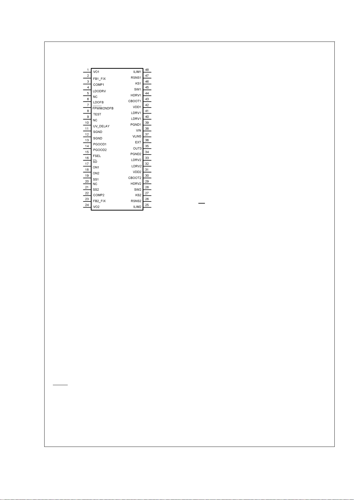
Connection Diagram
TOP VIEW
20015901
48-Lead TSSOP (MTD)
Order Number LM2645MTD
See NS Package Number MTD48
Pin Descriptions
VO1 (Pin 1):The feedback input for Channel 1. Always con-
nect directly to the output. Fixed or adjustable output voltage
is selected by FB1_FIX.
FB1_FIX (Pin 2): The feedback input for setting the output
voltage of Channel 1. Connecting this pin to VLIN5 sets the
output voltage to 5V, or to the center of a voltage divider for
an adjustable output.
COMP1 (Pin 3): Compensation pin for Channel 1. This is the
output of the internal transconductance amplifier. The compensation network should be connected between this pin
and the signal ground, SGND.
LDODRV (Pin 4): The output of the adjustable linear regulator controller. Connects to the base of a PNP Pass transistor. This pin is activated when Channel 1 is enabled.
NC (Pins 5, 9, 20): No internal connection. Connect these
pins to ground.
LDOFB (Pin 6): Dual function input pin. When connected to
the center of a resistor divider, it serves as the 1.238V
feedback input for the LDODRV. Connecting this pin to
VLIN5 disables the LDODRV.
FPWM/2NDFB (Pin 7): Multi-function input pin. When held
HIGH (>2V), pulse-skipping mode is enabled for both
switching regulators. When held LOW (
<
0.8V), both regulators will function in Fixed Frequency PWM mode. This pin
can also be connected to the center of a resistor divider for
feedback regulation of a secondary winding voltage. In this
case, Ch 1 will operate in pulse-skipping mode when the
output is lightly loaded. If the linear regulator controller output is heavy loaded, the operating frequency in
pulse-skipping will be increased accordingly to maintain the
voltage at this pin to 1.5V or higher. Thus, the secondary
winding voltage will always have the necessary overhead
voltage for the linear regulator to maintain regulation.
TEST (Pin 8): Special purpose input pin for factory use only.
This pin must be connected to ground.
UV_DELAY (Pin 10): : A capacitor from this pin to ground
adjusts the delay of the undervoltage protection for the two
switching outputs and the linear regulated output controlled
by the LDODRV. The delay time is set by charging a capacitor to 2.3V from a 5µA current source. Pulling this pin to
ground disables undervoltage protection on these outputs.
SGND (Pin 11,12): Ground connection for the signal level
circuitry. It should be connected to the ground rail of the
system.
PGOOD1 (Pin 13): An open-drain power-good output for
Channel 1. It is ’LOW’ (low impedance to ground) whenever
the output voltage travels out of the
±
10% window. It stays
latched in a ’LOW’ state if the output travels beyond the
positive limit that trips the over-volatge protection.
PGOOD2 (Pin 14): An open drain power good output for
Channel 2. It serves the same function as the PGOOD1.
FSEL (Pin 15): Selects the Switching Frequency of the two
switching controllers. The frequency is 300kHz when this pin
is pulled HIGH (
>
2V), or 200kHz when this pin is pulled
LOW (
<
0.8V).
SD (Pin 16): Shutdown control input. Pulling this pin LOW
(<0.6V) turns OFF the entire chip which then draws less
than 10 µA of supplycurrent. The chip isON if thispin is held
HIGH (
>
2V). Toggling this pin from HIGH to LOW and then
HIGH again resets the chip causing it to recover from any
protection latch.
ON1 (Pin 17): Output enable for Channel 1 and LDODRV
(Pin 4). Channel 1 and LDODRV are disabled when this pin
is pulled LOW (
<
0.8V), and are enabled when this pin is
pulled HIGH (
>
2V).
ON2 (Pin 18): Output enable for Channel 2. Channel 2 is
enabled when this pin is pulled high (
>
2V) and disabled
when this is pulled low (
<
0.8V).
SS1 (Pin 19): Soft-start input pin for Channel 1. The rise
time of the output voltage of Channel 1 is programmed by
the charge rate of a capacitor connected from this pin to
ground by an internal 2 µA current source. If the output does
not reach regulation (to within −6% of nominal voltage) by
the time this pin exceeds 2V (typical), the UV_DELAY pin
begins charging the capacitor connected from it to ground. If
the output is not within regulation after the UVP delay, the
chip latches off.
SS2 (Pin 21): Soft-start input pin for Channel 2. Serves the
same function as the SS1, Pin 19.
COMP2 (Pin 22): Compensation pin for Channel 2. This is
the output of the internal transconductance amplifier. The
compensation network should be connected between this
pin and the signal ground SGND (Pins 11, 12).
FB2_FIX (Pin 23): The feedback input for setting the output
voltage of Channel 2. Connecting this pin to VLIN5 sets the
output voltage to 3.3V,or to the center of a voltage divider for
an adjustable output.
VO2 (Pin 24): The feedback input for Channel 2. Always
connect directly to the output. Fixed or adjustable output
voltage is selected by FB2_FIX.
ILIM2 (Pin 25): Current limit threshold setting for Channel 2.
It sinks a constant current of 10 µA that is converted to a
voltage through a resistor connected from this pin to Vin. The
voltage across this resistor is compared with either the Vds
LM2645
www.national.com 2
Page 3

Pin Descriptions (Continued)
of the top MOSFET or the voltage across an external current
sense resistor to determine if an over-current condition has
occurred in Channel 2.
RSNS2 (Pin 26): The negative (−) Kelvin sense for the
internal current limit comparator of Channel 2. Always use a
separate trace to connect this pin to the current sense point.
Connect this pin to the low side of the current sense resistor
that is placed between V
IN
and the drain of thetop MOSFET.
When the Vds of the top MOSFET is used for current sensing, then connect this pin to the source of the top MOSFET.
KS2 (Pin 27): The positive (+) Kelvin sense for the internal
current limit comparator of Channel 2. Use a separate trace
to connect this pin to the current sense point. Connect to Vin
as close to the node of the current sense resistor; when no
current-sense resistor is used, connect it as close to the
Drain node of the upper MOSFET.
SW2 (Pin 28): : Switch-node connection for Channel 2,
which is connected to the source of the top MOSFET. It
serves as the negative supply rail for the topside gate driver,
HDRV2.
HDRV2 (Pin 29):Top-sidegate-drive output for Channel 2.A
floating drive output that rides on the switching-node voltage.
CBOOT2 (Pin 30): Bootstrap capacitor connection. It serves
as the positive supply rail for the Channel 2 top-side gate
drive.
VDD2 (Pin 31): The supply rail for the Channel 2 low-side
gate drive, usually ties together with VDD1. Connect to
VLIN5 through a 4.7Ω resistor and bypassed to ground with
a ceramic capacitor of at least 1µF.
LDRV2 (Pins 32, 33): Low-side gate-drive output for Channel 2. Tie these two pins together.
PGND2 (Pin 34): Power ground for Channel 2.
OUT3 (Pin 35): The fixed 3.3V linear regulated output. De-
rived from VLIN5 by an internal LDO, it is current limited at
100mA. The continuous output current is a function of the
ambient operating temperature and the total power dissipation in the chip and must be derated accordingly. See (Note
2) in Electrical Characteristics section.
EXT (Pin 36): External power input to an internal switch.
This pin is usually connected to the fixed 5V output of
Channel 1. When the voltage on this pin is higher than 4.7V,
the internal 5V LDO that provides VLIN5 from VIN is disabled, and an internal switch connects VLIN5 to this pin to
minimize dissipation in the chip. Connect this pin to ground
and VLIN5 to VIN if VIN is operating in 4.5V to 5.5V range.
VLIN5 (Pin 37): This pin is the output of an internal 5V LDO
regulator derived from VIN when no external 5V supply is
available. It supplies the internal bias for the chip, supplies
the boostrap circuitry for gate drive and serves as the input
supply of an internal LDO to generate OUT3.Bypass this pin
to power ground with a minimum of 4.7µF ceramic capacitor.
Connect this pin to the VIN pin when Vin is operating in 4.5V
to 5.5V range.
VIN (Pin 38):The input power of the chip. Connects to the
upper (+) input rail of the system.
PGND1 (Pin 39):Power ground for Channel 1.
LDRV1 (Pins 40, 41): Low-side gate-drive output for Chan-
nel 1. Tie these two pins together.
VDD1 (Pin 42): The supply rail for the low-side gate drive of
Channel 1. Same function as VDD2 (Pin 31).
CBOOT1 (Pin 43): Bootstrap capacitor connection. It serves
as the positive supply rail for the Channel 1 top-side gate
drive.
HDRV1 (Pin 44): Top-side gate-drive output for Channel 1.
See HDRV2 (Pin 29).
SW1 (Pin 45): Switch-node connection for Channel 1, See
SW2 (Pin 28).
KS1 (Pin 46): The upper (+) Kelvin sense for the internal
current limit comparator of Channel 1 (see KS2, Pin 27).
RSNS1 (Pin 47): The lower (−) Kelvin sense for the internal
current limit comparator of Channel 1 (see RSNS2, Pin 26).
ILIM1 (Pin 48): Current limit threshold setting for Channel 1
(see ILIM2, Pin 25).
LM2645
www.national.com3
Page 4
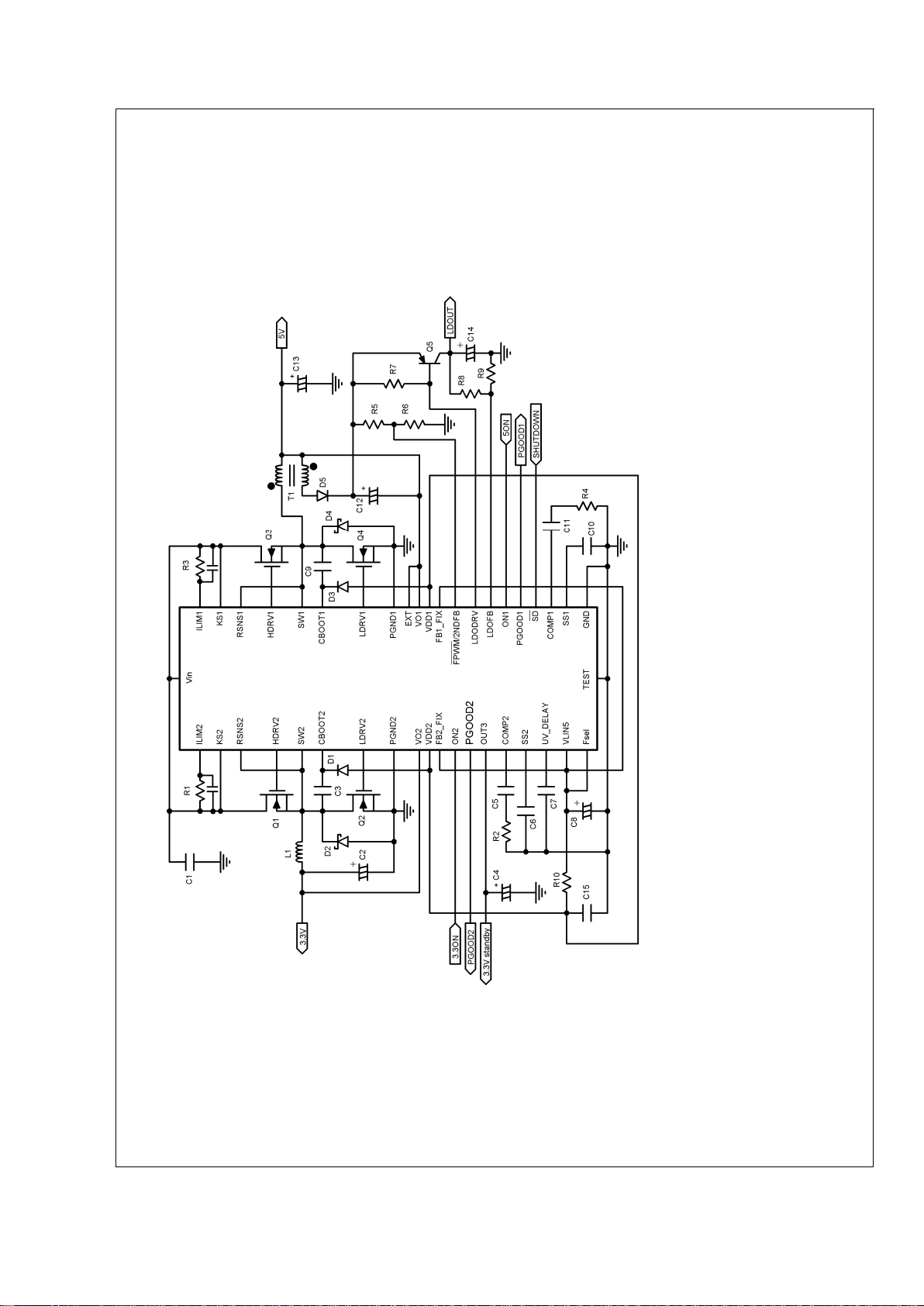
Typical Application Circuit
20015902
LM2645
www.national.com 4
Page 5

Simplified Block Diagram
20015905
LM2645
www.national.com5
Page 6

Simplified Block Diagram (Continued)
20015903
LM2645
www.national.com 6
Page 7

TABLE 1. Shut Down Latch Truth Table
Input Output
ovp1 ovp2 uvp1 uvp2 uvp4 oc3 ch1 on ch2 on fault ssto1 ssto2 uv_delay latch off
1101
1101
1 1 0 1 cap 1
1 1 0 1 cap 1
1 1 0 1 cap 1
000001 000cap 0
All other combinations 0
Notes:
1. ’fault’ is the logic OR of UVLO and thermal shutdown.
2. ’cap’ means the pin has a capacitor of appropriate value between it and ground.
3. Positive logic is used.
4. ssto1, ssto2 means soft start timeout for Ch 1 and Ch 2 respectively.
5. A blank value means ’don’t care’.
6. ″oc3″ means OUT3 output current over 100mA current.
7. ″uvp4″ means UVP of the linear regulated output controlled by LDODRV.
8. SD pin is pulled high.
TABLE 2. Power Good Truth Table
Input Output
ovp1 ovp2 uvpg1 uvpg2 uvpg4 ch1 on ch2 on fault latch
off
SD
PGOOD1 PGOOD2
1 1 1100
1 1 1100
11 10
11 10
00110011
010
010
00 10011
0 0 100 1 1
1 100
1100
000
Notes:
1. Positive logic is used.
2. A blank value means ’don’t care’.
3. The symbol uvpg1, 2, 4 means the power good undervoltage threshold of the corresponding channel.
LM2645
www.national.com7
Page 8

Absolute Maximum Ratings (Note 1)
If Military/Aerospace specified devices are required,
please contact the National Semiconductor Sales Office/
Distributors for availability and specifications.
Voltages from the indicated pins to SGND/PGND:
VIN, ILIM1, ILIM2, KS1, KS2,
LDODRV −0.3V to 31V
SW1, SW2, RSNS1, RSNS2 −0.3 to (V
IN
+
0.3)V
VO1, VO2, FB1_FIX, FB2_FIX,
VDD1, VDD2, EXT −0.3V to 6V
SD, ON1, SS1, ON2, SS2, LDOFB,
F
SEL
, UV_DELAY, PGOOD1, OUT3,
PGOOD2, COMP1, COMP2,
FPWM/2NDFB
−0.3V to (VLIN5
+0.3)V
CBOOT
1
to SW1, CBOOT2 to SW2 −0.3V to 7V
LDRV1, LDRV2 −0.3V to
(VDD+0.3)V
HDRV1 to SW1, HDRV2 to SW2 −0.3V
HDRV1 to CBOOT1, HDRV2 to
CBOOT2 +0.3V
Power Dissipation (T
A
= 25˚C,
(Note 2) 1.56W
Junction Temperature (T
J
)
(Note 2) +150˚C
Ambient Storage Temperature
Range −65˚C to +150˚C
Soldering Dwell Time, Temperature
(Note 3)
Wave
Infrared
Vapor Phase
4 sec, 260˚C
10sec, 240˚C
75sec, 219˚C
ESD Rating (Note 4) 2kV
Operating Ratings(Note 1)
VIN (VIN and VLIN5 separate) 5.5V to 30V
VIN (VLIN5 tied to VIN) 4.5V to 5.5V
Junction Temperature 0˚C to +125˚C
EXT 5.5V max.
Electrical Characteristics
Unless otherwise specified, VIN= 15V, SGND = PGND = 0V, VLIN5 = VDD1 = VDD2. Limits appearing in boldface type apply over the entire operating junction temperature range, 0˚C to +125˚C. Specifications appearing in plain type are measured
using low duty cycle pulse testing with T
A
= 25˚C (Note 5), (Note 6). Min/Max limits are guaranteed by design, test, or statisti-
cal analysis.
Symbol Parameter Conditions Min Typ Max Units
SYSTEM
∆V
OUT/VOUT
Load Regulation VIN=15V, V
compx
= 0.5V to 1.5V 0.04 %
∆V
OUT/VOUT
Line Regulation 5.5V ≤ VIN≤ 30V, V
compx
=1.25V 0.04 %
V
FBX_FIX
Feedback Voltage in
Adjustable Mode
5.5V ≤ VIN ≤ 30V
1.217 1.238 1.259 V
V
OUT
V
OUTx
accuracy at fixed
output mode
5.5V ≤ VIN≤ 30V, V
OUT1
= 5V, V
OUT2
= 3.3V
−2.4 +2.4 %
I
VIN
Input Supply Current ON1 = ON2 = 5V and
5.5V ≤ V
IN
≤ 30V
1.5 2.8 mA
ON1 = ON2 = 5V and
4.5V ≤ V
IN
= VLIN5 ≤ 5.5V
1.3 2.8 mA
Standby (Note 7)
ON1 = ON2 = 0V, V
SD
=5V
50 120 µA
Shutdown V
SD
=0V 5 30 µA
VLIN5 VLIN5 Output
Voltage(Note 8)
IVLIN5 = 0 to 25mA, EXT = 0V,
5.5V ≤ VIN ≤ 30V, SD = 5V
4.65 5 5.35 V
V
CLos
Current Limit
Comparator Offset
(VILIMX −VRSNSX)
VKS1−VILIM1 = VKS2-VILIM2
=140mV
±
2mV
I
CL
Current Limit Sink
Current
8 10 12 µA
I
ss_SC
Soft-Start Source
Current
V
ss1=Vss2
=1V
0.5 2 3.5 µA
I
ss_SK
Soft-Start Sink Current V
ss1=Vss2
=1V 24 µA
V
ssto
Soft-Start Timeout
Threshold
(Note 9)
2V
LM2645
www.national.com 8
Page 9

Electrical Characteristics (Continued)
Unless otherwise specified, VIN= 15V, SGND = PGND = 0V, VLIN5 = VDD1 = VDD2. Limits appearing in boldface type apply over the entire operating junction temperature range, 0˚C to +125˚C. Specifications appearing in plain type are measured
using low duty cycle pulse testing with T
A
= 25˚C (Note 5), (Note 6). Min/Max limits are guaranteed by design, test, or statisti-
cal analysis.
Symbol Parameter Conditions Min Typ Max Units
SYSTEM
V
UVP
FB1_FIX, FB2_FIX,
LDOFB Undervoltage
Protection Latch
Threshold
As a Percentage of nominal output
voltage (Falling edge)
73 80 90 %
Hysteresis 4%
V
UV_DELAY
UV_DELAY Threshold
Voltage
(Note 10)
2.3 V
I
UV_DELAY
UV_DELAY source
current
V
UV_DELAY
=2V
5µA
V
OVP
V
OUTx
Overvoltage
Protection Latch
Threshold
As a percentage measured at
FB1_FIX, FB2_FIX 106 110 119 %
TH
LREG
V
OUTx
Low Regulation
Comparator Enable
Threshold for channels 1
and 2
Falling Edge
95 %
HYS
LREG
Hysteresis of Low
Regulation Comparator
As a Percentage of output voltage
3%
V
pwrbad
Regulator Window
Detector Thresholds
(PGOOD from High to
Low) (Note 11)
As a Percentage of output voltage
86 91 94 %
V
pwrgd
Regulator Window
Detector Thresholds
(PGOOD from Low to
High)
As a Percentage of output voltage
92.5 94 96.5 %
TH
VOX_DIS
VO1, VO2 Quick
Discharge Threshold
(Note 12)
0.8 V
V
ox_R
VO1,VO2
ON-Resistance
VO1=VO2=2V
200 Ω
Gate Drive
I
CBOOT
CBOOT Leakage
Current
V
CBOOT1
=V
CBOOT2
=7V
100 nA
I
SC_DRV
HDRVx and LDRVx
Source Current
V
CBOOT1
=V
CBOOT2
= 5V, VSWx=0V,
HDRVx=LDRVx=2.5V
0.8 A
I
sk_HDRV
HDRVx Sink Current V
CBOOTx
= VDDx = 5V, V
SWx
= 0V,
HDRVX = 2.5V
1.3 A
I
sk_LDRV
LDRVx Sink Current V
CBOOTx
= VDDx = 5V, V
SWx
= 0V,
LDRVX = 2.5V
2.5 A
R
HDRV
HDRV1 & 2 Source
On-Resistance
V
CBOOT1
=V
CBOOT2
= 5V,
V
SW1=VSW2
=0V
2.2 Ω
HDRV1 & 2 Sink
On-Resistance
1.1 Ω
R
LDRV
LDRV1 & 2 Source
On-Resistance
V
CBOOT1
=V
CBOOT2
= 5V,
V
SW1=VSW2
=0V
2.2 Ω
LDRV1 & 2 Sink
On-Resistance
0.65
Ω
LM2645
www.national.com9
Page 10

Electrical Characteristics (Continued)
Unless otherwise specified, VIN= 15V, SGND = PGND = 0V, VLIN5 = VDD1 = VDD2. Limits appearing in boldface type apply over the entire operating junction temperature range, 0˚C to +125˚C. Specifications appearing in plain type are measured
using low duty cycle pulse testing with T
A
= 25˚C (Note 5), (Note 6). Min/Max limits are guaranteed by design, test, or statisti-
cal analysis.
Symbol Parameter Conditions Min Typ Max Units
SYSTEM
Oscillator
F
osc
Oscillator Frequency F
SEL
=5V 265 300 335 kHz
F
SEL
=0V 174 200 226 kHz
Don_max Maximum On-Duty Cycle V
FB1=VFB2
= 1V, Measured at pins
HDRV1 and HDRV2
96 98 %
T
on_min
Minimum On-Time 150 ns
Error Amplifier
I
FB1,IFB2
Feedback Input Bias
Current
V
FB1_FIX
= 1.5V, V
FB2_FIX
= 1.5V
90 250 nA
I
comp1_SC
,
I
comp2_SC
COMP Output Source
Current
V
FB1_FIX
=V
FB2_FIX
= 1V,
V
COMP1
=V
COMP2
=1V
27 104 µA
I
comp1_SK
,
I
comp2_SK
COMP Output Sink
Current
V
FB1_FIX
=V
FB2_FIX
= 1.5V and
V
COMP1
=V
COMP2
= 0.5V
27 99 µA
Voltage References and Linear Voltage Regulators
UVLO VLIN5 Under-voltage
Lockout Threshold
(Rising)
SS1, SS2 transition from low to high
3.6 4.0 4.4 V
R_EXT EXT pin ON-Resistance V
EXT
= 5V, IVLIN5=25mA 3 Ω
EXT_TH VLIN5-to-EXT Switch
Over Threshold
Rising edge of V
EXT
4.7 V
V
OUT3
3.3V Linear Regulator
Output Voltage
0mA<IOUT3<50mA, 5.5V ≤ VIN ≤
30V, V
EXT
=5V
3.306 3.3 3.564 V
I
OUT3
3.3V Linear regulator
Current limit threshold
ON1 = HIGH, EXT = 5V
100 mA
I
LDODRV
LDODRV pin Sink
Current
V
LDODRV
= 11V, V
LDOFB
= 1.1V
4.0 6mA
V
LDOFB
LDODRV Feedback
Voltage
3.5V ≤ V
LDODRV
≤ 12V
1.215 1.240 1.265 V
Accuracy with Load 3.5V ≤ LDO power supply voltage ≤
15V, I
LDODRV
= 500µA
1.236 V
I
LDOFB
LDOFB Leakage Current
(Sourcing)
V
LDOFB
= 1.4V
50 100 nA
V
2NDFB
Secondary winding
voltage feedback detect
threshold
Falling Edge
1.3 1.5 1.7 V
Logic Inputs
V
IH
Minimum High Level
Input Voltage (SD,
FPWM/2NDFB, ON1,
ON2, F
SEL
)
2.0 V
V
IL
Maximum Low Level
Input Voltage for
FPWM/2NDFB, ON1
ON2, F
SEL
)
0.8 V
SD
0.6 V
LM2645
www.national.com 10
Page 11

Electrical Characteristics (Continued)
Unless otherwise specified, VIN= 15V, SGND = PGND = 0V, VLIN5 = VDD1 = VDD2. Limits appearing in boldface type apply over the entire operating junction temperature range, 0˚C to +125˚C. Specifications appearing in plain type are measured
using low duty cycle pulse testing with T
A
= 25˚C (Note 5), (Note 6). Min/Max limits are guaranteed by design, test, or statisti-
cal analysis.
Symbol Parameter Conditions Min Typ Max Units
SYSTEM
I
IL
Maximum Input Leakage
Current (SD,
FPWM/2NDFB, ON1,
ON2, FSEL).
Logic Input Voltage 0 or 5V
±
0.1 µA
Logic Outputs
I
OL
PGOOD Low Sink
Current
V
PGOOD
= 0.4V
1.4 mA
I
OH
PGOOD High Leakage
Current
V
PGOOD
=5V
50 200 nA
Note 1: Absolute maximum ratings indicate limits beyond which damage to the device may occur. Operating Ratings are conditions under which operation of the
device is guaranteed. For guaranteed performance limits and associated test conditions, see the Electrical Characteristic tables.
Note 2: Maximum allowable power dissipation is calculated by using P
DMAX
=(T
JMAX-TA
)/θJA, where T
JMAX
is the maximum junction temperature, TAis the
ambient temperature and θ
JA
is the junction-to-ambient thermal resistance of the specified package. The 1.56W rating results from using 150˚C, 25˚C, and 80˚C/W
for T
JMAX,TA
, and θJArespectively. A θJAof 90˚C/W represents the worst-case condition of no heat sinking of the 48-pin TSSOP. Heat sinking allows the safe
dissipation of more power. The Absolute Maximum power dissipation should be derated by 12.5mW per ˚C above 25˚C ambient. The LM2645 actively limits its
junction temperature to about 150˚C.
Note 3: For detailed information on soldering plastic small-outline packages, refer to the Packaging Databook available from National Semiconductor Corporation.
Note 4: Except for SW1, SW2, CBOOT1 and CBOOT2 pins which are 1.5kV. For testing purposes, ESD was applied using the human-body model, a 100pF
capacitor discharged through a 1.5kΩ resistor.
Note 5: A typical is the center of characterization data measured with low duty cycle pulse tsting at T
A
= 25˚C. Typicals are not guaranteed.
Note 6: All limits are guaranteed.All electrical characteristics having room-temperature limits are tested during production with T
A=TJ
= 25˚C. All hot and cold limits
are guaranteed by correlating the electrical characteristics to process and temperature variations and applying statistical process control.
Note 7: Both switching controllers are OFF. The linear regulators VLIN5 and 3OUT remain ON.
Note 8: The output voltage at the VLIN5 pin may be as high as 6.5V in shutdown mode (SD ≤ 0.6V).
Note 9: When SS1, SS2 pins are charged above this voltage and either of the output voltage at V
OUT1
or V
OUT2
is still below the regulation limit, the under voltage
protection feature is initialized.
Note 10: Above this voltage, the under voltage protection is enabled.
Note 11: Foreach device, there is a 10% (typical) gap of the measured output voltage between the PGOOD signal transitions from high to low and the under voltage
protection is activated. The under voltage protection will not be activated while the PGOOD signal is in the logic HIGH state.
Note 12: During normal shutdown or UVP, LDRV1or LDRV2 pin goes high when VO1, VO2 detects an output voltage below this level.
LM2645
www.national.com11
Page 12

Typical Performance Characteristics
Efficiency vs Load Current
(FPWM/2NDFB = VLIN5)
Efficiency vs Load Current
(FPWM/2NDFB = VLIN5)
20015906 20015907
Efficiency vs Load Current
(FPWM/2NDFB = VLIN5)
Quiescent Current vs Supply Voltage
20015908
20015912
Reference Voltage vs Temperature
(Bandgap + Error Amplifier Offset)
Error Amplifier Gm vs Temperature
(V
IN
= 15V)
20015910
20015911
LM2645
www.national.com 12
Page 13

Typical Performance Characteristics (Continued)
Switching Frequency vs Load Current
(FPWM/2NDFB = VLIN5)
Normalized Switching Frequency vs Temperature
(F
OSC
= 300 kHz)
20015909
20015913
VLIN5 Output vs Temperature
OUT3 vs Temperature
(VIN= 15V, EXT = Vo1 = 5V, ON1 = On, ON2 = Off)
20015914 20015915
Shutdown Waveforms
(V
OUT
= 3.3V, I
OUT
= 0A)
Shutdown Waveforms
(V
OUT
= 5V, I
OUT
= 3A)
20015916
20015917
LM2645
www.national.com13
Page 14

Typical Performance Characteristics (Continued)
Load Transient Response
(V
IN
= 10V, V
OUT
= 3.3V, L = 6.0 µH, C
OUT
=
180µF/15mΩ)
Load Transient Response
(V
IN
= 10V, V
OUT
= 1.8V, L = 3.1 µH, C
OUT
=
270µF/15mΩ)
20015918
20015919
Overcurrent and Undervoltage Protection
(V
OUT1
= 5V, V
OUT2
= 3.3V)
Pulse-Skipping Operation
(VIN= 15V, V
OUT
= 5V, I
OUT
= 35mA)
20015920
20015921
Soft Start
(V
IN
= 10V to 28V, V
OUT
= 5V, I
OUT
=0Ato3A)
Start Up at Sleep Mode
(VIN= 15V, ON1 = ON2 = Off)
20015922
20015923
LM2645
www.national.com 14
Page 15

Operation Descriptions
General
The LM2645 integrates two synchronous switching controllers, one adjustable linear regulator controller and one fixed
3.3V output into a single package. It solves the need within
many portable systems for 5V, 3.3V, 3.3V stand-by and 12V
legacy power supplies.
The two switching controllers, Channel 1 and Channel 2,
operate 180˚ out of phase to reduce input capacitor size and
cost. They can be independently enabled and disabled. The
external linear regulator controller, or Channel 4,can also be
independently enabled and disabled when Channel 1 has
been enabled.
The output voltages of channel 1 and channel 2 can be set
between 1.3V to 5.5V by external voltage divider, or fixed at
5V and 3.3V respectively without the need of external voltage divider. The output voltage of Channel 4 is adjustable
from 3.3V to 15V.
Both switching channels use synchronous rectification and
employ a peak current mode control scheme. Protection
features include over-voltage protection (Ch1 and 2),
under-voltage protection (Ch1, 2 and 4), and positive and
negative peak current limit (Ch1 and 2).UVP function can be
disabled or delayed by an arbitrary amount of time. The
device operates with a wide input voltage range from 5.5V to
30V. The outputs of the two switching channels have independent power good monitoring. Channel 1 and channel 2
can be configured to operate in parallel as a dual phase
switching converter for high power applications
Soft Start
In normal operation the soft-start functions as follows.As the
input voltage rises above the 4.2V UVLO threshold, the
internal circuitry is powered on, aninternal 2µA current starts
to charge the capacitor connected between the SSx pin and
ground, and the corresponding channel is turned on. A MIN_ON_TIME comparator generates the soft start PWM
pulses. As the SSx pin voltage ramps up, the duty cycle
increases, causing the output voltage to ramp up. Duringthis
time, the error amplifier output voltage is clamped at 0.8V,
and the duty cycle generated by the PWM comparator is
ignored. When the corresponding output voltage exceeds
98.5% (typical) of the set target voltage, the regulator transitions from soft-start to operating mode. Beyond this point,
once the PWM pulses generated by the PWM comparator
are wider than those generated by the MIN_ON_TIME comparator, the PWM comparator takes over and starts to regulate the output voltage. At the same time, the high clamp at
the output of the error amplifier is switched to 2V. That is,
peak current mode control now takes place.
The rate at which the duty cycle increases depends on the
capacitance of the soft start capacitor. The higher the capacitance, the slower the output voltage ramps. A unique
feature of the LM2645 is that the rate at which the duty cycle
grows is independent of the input voltage. This is because
the ramp signal used to generate the soft start duty cycle has
a peak value proportional to the input voltage, making the
product of duty cycle and input voltage a constant. This
makes the soft start process more predictable and reliable.
During soft start, under-voltage protection istemporarily suspended, but over-voltage protection and current limit remain
in effect. When the SSx pin voltage exceeds 2V, a soft start
time out signal (sstox) will be issued. This signal sets the
under-voltage protection into ready mode. See the
Under-Voltage Protection section.
If either the SS1 or SS2 pin is short-circuited to ground
before startup, the corresponding channel will operate at
minimum duty cycle when it is enabled, and the
under-voltage protection of that channel will be disabled.
However, if the soft start has been completed and the output
voltage has been established, then short-circuiting the SSx
pin to ground does not affect the normal operation and
under-voltage protection of that channel.
Shut Down Latch State
This state is typically caused by an output under-voltage or
over-voltage event. In this state, both switching channels
have their top FETs turned off and their bottom FETs turned
on (See the Ch1 and 2 output capacitors discharge section).
The LDODRV pin will be shut down, but VLIN5 and OUT3
will remain unaffected.
There are two methods to release the system from the latch
off state. One is to cycle theinput voltage. Another method is
to pull the SD pin below 0.6V and release it HIGH again.
After the latch is released, the two switching channels will go
through the normal soft start process.
Ch 1 and 2 Output Capacitors Discharge
Each switching channel has an embedded 200Ω MOSFET
with the drain connected to the VOx pin. This MOSFET will
discharge the output capacitor of that channel if that channel
is turned off due to one of the following events:
1. Its ONx pin is pulled low to below 0.8V.
2. The IC enters shut down mode or fault state.
3. The IC enters shut down latch state causedby an output
under-voltage event.
When the output capacitor has been discharged to about
0.8V, the bottom gate-drive (LDRVx) will be turned on, driv-
ing on the bottom FET to discharge the output capacitor
through the filter inductor.
If an output over-voltage event occurs, the HDRVx will be
turned off and the LDRVx will be turned on immediately
regardless of the level of output voltage, thus discharging the
output capacitor through the filter inductor.
When that channel is released from theshutdown latchstate
or returned to the on state, it will go through the soft start
process to recover the output voltage.
Fault State
If the input voltage drops to less than 3.9V, or the IC enters
thermal shut down mode, a ″fault″ signal will be generated
internally.This signal will discharge the capacitor connected
between the SSx pin and ground with 24µA of current until
the SSx pin reaches 50mV. This will turn off both switching
channels.
Force PWM Mode
This mode applies to both switching channels simultaneously. The force-PWM mode is activated by pulling the
FPWM/2NDFB pin to logic low. In this mode, the top FET
and the bottom FET gate signals are always complementary
to each other and the NEGATIVE CURRENT LIMIT comparator is activated (see
Negative Current Limit
section). In
force-PWM mode, the regulator always operates in Continuous Conduction Mode (CCM) and its duty cycle (approximately Vout / Vin) is almost independent of load.
LM2645
www.national.com15
Page 16

Operation Descriptions (Continued)
The force-PWM mode is good for applications where fixed
switching frequency is required.
In force-PWM mode, the top FET has to be turned on for a
minimum of typically 220ns each cycle. However, when the
required duty cycle is less than the minimum value, the skip
comparator will be activated and pulses will be skipped to
maintain regulation.
Skip Comparator
Whenever the output voltage of the error amplifier (COMPx
pin) goes below a 0.5V threshold, the PWM cycles will be
″skipped″ until that voltage exceeds the threshold again.
Pulse-Skip Mode
This mode is activated by pulling the FPWM/2NDFB pin to a
TTL-compatible logic high and applies to both switching
channels simultaneously. In this mode, the 0-CROSSING /
NEGATIVECURRENT LIMIT comparator detects the bottom
FET current. Once the bottom FET current flows from drain
to source, the bottom FET will be turned off. This prevents
negative inductor current. In force-PWM operation, the inductor current is allowed to go negative, so the regulator is
always in Continuous Conduction Mode (CCM), no matter
what the load is. In CCM, duty cycle is almost independent of
the load and is roughly Vout divided by Vin. In pulse-skip
mode, the regulator enters Discontinuous Conduction Mode
(DCM) under light load. Once the regulator enters DCM, its
switching frequency droops as the load current decreases.
The regulator operates in DCM PWM mode until its on-time
falls below 85% of the CCM on-time, then the MIN_ON_TIME comparator takes over. It forces 85% of the CCM
on-time thus causing the output voltage to continuously rise
and COMPx pin voltage (error amplifier output voltage) to
continuously droop. When the COMPx pin voltage hits the
0.5V level, the CYCLE_SKIP comparator toggles, causing
the present switching cycle to be ″skipped″, i.e., both FETs
remain off during the whole cycle.As long as the COMPx pin
voltage is below 0.5V, no switching of the FETs will happen.
As a result, the output voltage will droop, and the COMPx pin
voltage will rise. When the COMPx pin goes above the 0.5V
level, the CYCLE_SKIP comparator flips and allows a 85%
CCM on-time pulse to happen. If the load current is so small
that this single pulse is enoughto bring theoutput voltage up
to such a level that the COMPx pin drops below 0.5V again,
the pulse skipping will happen again. Otherwise it may take
a number of consecutive pulses to bring the COMPx pin
voltage down to 0.5V again. As the load current increases, it
takes more and more consecutive pulses to drive the
COMPx voltage to 0.5V. When the load current is so high
that the duty cycle exceeds the 85% CCM on-time, then
pulse-skipping disappears. In pulse-skip mode, the frequency of the switching pulses decrease as the load current
decreases. Since the load is usually very light in pulse-skip
mode, conducted noise will be very low and the variable
operating frequency should cause no EMI problems in the
system.
The LM2645 pulse-skip mode helps the light load efficiency
for two reasons. First, it turns on the bottom FET only when
inductor current is in positive conduction region, this eliminates circulating energy loss. Second, the FETs are switching only when necessary, rather than every cycle, that reduces FETs switching loss and gate drive power loss.
Current Sensing and Current Limiting
The information of inductor current is extracted by the current sense pin KSx and RSNSx. As shown in
Figure 1
and
Figure 2
, current sensing is accomplished by either sensing
the Vds of the top FET, or sensing the voltage across a
current sense resistor connected from Vin to the drain of the
top FET. The advantage of sensing current across the top
FET is reduced parts count and cost. Using a current sense
resistor improves current sense accuracy. To ensure linear
operation of the current amplifier, the current sense voltage
input must not exceed 200mV. Therefore, the Rds of the top
FET or the current sense resistor must besmall enough that,
when the top FET is on, the current sense voltage does not
exceed 200mV.
There is a leading edge blanking circuit that forces the top
FET to be on for at least 150ns. Beyond this minimum on
time, the output of the PWM comparator is used to turn off
the top FET.
With an external resistor connected between the ILIMx pin
and the KSx pin, the 10µA current sink on the ILIMx pin
produces a voltage across the resistor to serve as the reference voltage for current limit. Adding a 10nF capacitor
across this resistor will filter unwanted noise that could improperly trip the current limit comparator. Current limit is
activated if the inductor current is too high causing the
voltage at the RSNSx pin to be lower than that of the ILIMx
pin, toggling the comparator thus turning off the top FET
immediately.The comparator is disabled either when the top
FET is turned off or during the leading edge blanking time.
20015928
FIGURE 1. Current Sensing by Vds of the Top FET
20015929
FIGURE 2. Current Sensing by External Sense Resistor
LM2645
www.national.com 16
Page 17

Operation Descriptions (Continued)
Negative Current Limit
The purpose of negative current limit is to ensure that the
inductor will not saturate during negative current flow causing excessive current to flow through the bottom FET. The
negative current limit is realized through sensing the bottom
FET Vds. An internally generated 100mV (typical) is used to
compare with the bottom FET Vds when it is on. Upon
sensing too high a Vds, the bottom FET will be turned off.
The negative current limit is activated in force PWM mode.
Over-Voltage Protection
This protection feature is implemented in the two switching
channels and not the linear channels.Any over voltage event
at any of the two switching channels’ output will cause the
LM2645 to enter the
shut down latch state
. The HDRVx will
be turned off, and the LDRVx will be turned on immediately
to drive the bottom FET to discharge the output capacitor
through the filter inductor.
Under-Voltage Protection
The UVP feature is implemented in channel 1, channel 2 and
the linear regulator controller (LDODRV). The under-voltage
protection feature is disabled if the UV_DELAY pin is pulled
to ground; this is useful forsystem debug work.If a capacitor
is connected between the UV_DELAY pin and ground, and
the voltage at the SSx pin is above 2V, the UVP is at ready
mode.
If a switching channel is enabled, and its soft-start time out
signal, sstox (see soft start section) is asserted, then an
under-voltage event at the output of that channel will cause
the system to enter the UVP timeout state. For the external
linear regulator controller (LDODRV), if channel 1 is on and
the soft start time out signal (ssto1) has been issued, then an
under voltage event at the linear regulator output will cause
the system to enter UVP timeout state.
When the system reacts on an under-voltage event, a 5µA
current will charge the capacitor connected to the UV_DELAYpin; when the capacitor is charged to a voltage exceeding 2.3V(typical), the system immediately enters shut down
latch state.
Power Good Function
Two power good signals are available for indicating the
general health of the two switching channels individually.
The function is realized through the internal MOSFET of
each channel tied from the PGOODx pins to ground. The
power good signal is asserted by turning off the MOSFET of
that channel. The on resistance of the power good MOSFET
is about 300Ω.
The internal power good MOSFET will not be turned on
unless at least one of the following occurs:
1. there is an output over voltage event;
2. the output voltage is below the power good lower limit;
3. system is in the shut down mode, i.e. the SD pin voltage
is below 0.6V;
4. The switching channel is in standby mode, i.e. the ONx
pin is below 0.8V;
5. system is in the
fault state
.
6. system is in the
shut down latch state
.
Power good upper limit is the same as that of the OVP
threshold.
Except in the latched off condition (cases 1 and 6) , if the
corresponding output voltage(s) recovers to within −6% of
regulation, PGOODx will be asserted again. But there is a
built-in hysteresis. See V
pwrgd
in the Electrical Characteris-
tics table. The above information is also available in
Power
Good Truth Table
.
VLIN5, VDDx and EXT
An internal 5V supply (VLIN5) is generated from the VIN
voltage through an internal linear regulator. This 5V supplyis
mainly for internal circuitry use, but can also be used externally. When used externally, it is recommended that the
VLIN5 voltage only be used for powering the gate drivers,
i.e. supplying the bias for the top drivers’ bootstrap circuit
and the bottom drivers’ VDDx pins.
When the voltage applied to the EXT pin is below 4.7V, an
internal 5V low dropout regulator supplies the power for the
VLIN5. If the EXT voltage is taken above 4.7V, the 5V
regulator is turned off and an internal switch is turned on to
connect the EXT pin to the VLIN5 pin. This allows the VLIN5
power to be derived from a high efficiency source such as
the output from either one of the switching channels, when
the channel is configured to operate in fixed 5V mode.
Irrespective of the signals on the ONx pins, the VLIN5 voltage output will come from the EXT pin whenever the voltage
applied to the EXT pin is higher than 4.7V. The externally
applied voltage is required to be less than the voltage applied to the VIN pin at all times, even when both channels are
shut down. This prevents a voltage back feed situation from
the EXT pin to the VIN pin.
In shut down mode the VLIN5 pin may go as high as 6.5V.
Connecting a 100kΩ dummy load from VLIN5 to ground will
hold the voltage to 6V maximum. Using a 200kΩ resistor to
pull up PGOOD1 and PGOOD2 to VLIN5 is an alternative
solution.
When input voltage is guaranteed to be within 4.5V to 5.5V,
tie the VLIN5 pin directly to the VIN pin and tie the EXT to
ground. In this mode, the VLIN5 current directly comes from
power stage input rail and power loss due to the internal
linear regulation is no longer an issue.
The two VDDx pins can be tied together. Always connect
them to the VLIN5 pin through a 4.7Ω resistor and connect a
ceramic capacitor of at least 1µF to bypass theVDDx pinsto
ground.
Output Capacitors For Linear Regulators
Like any linear regulator, each linear output that is either
generated or controlled by the LM2645 requires an output
capacitor to ensure stability. The output of OUT3 needs a
capacitor of 1µF minimum. The VLIN5 needs a minimum of
4.7µF. Channel 4, the linear regulated output rail that is
controlled by the LDODRV pin, requires an output capacitor
of 10µF minimum to prevent oscillation.
In applications where the OUT3 is not needed, it may be
disabled by connecting this pin to the VLIN5 as illustrated in
Figure 3
to eliminate the need of a output capacitor.
LM2645
www.national.com17
Page 18

Operation Descriptions (Continued)
Likewise, if the LDODRV pin is not used, connect the LDOFB pin to VLIN5 as shown in
Figure 4
to disable this
channel and the under voltage protection associated with it.
Switching Noise Reduction
Power MOSFETs are very fast switching devices. In synchronous rectifier converter, rapid drain current rise rate of
the top FET coupled with parasitic inductance will generate
unwanted Ldi/dt spikes noise at the source node of the FET
(SWx node). The magnitude of the spike noise will increase
as the output current increases. This parasitic spike noise
may turn into electromagnetic interference (EMI) that may
cause trouble to the system performance, therefore, mustbe
suppressed.
As shown in
Figure 5
, adding a resistor in series with the
CBOOTx pin will slowdown the gate drive (HDRVx) rise time
of the top FET to yield a desired drain current transition time.
Usually a 3.3 to 5.1 ohm resistor is sufficient to suppress the
noise. The top FET switching loss will increase with higher
resistance values.
Input Power Supply Cycling
If the input supply is removed during operation and then
re-applied before the power-on-reset signal has been reset,
the part will remain latched off.A solution for this problem is
shown in
Figure 6
, using a voltage divider of 4:5 ratio to pull
the SD pin up to VLIN5. With the voltage divider, the SD pin
always falls below the logic low level and executes the
power-on-reset after VIN drops below 3V. External shudown
control is included as an option.
Dual-Phase Parallel Outputs
In applications with high output current demand, the two
switching channels can be configured to operate as a
two-phase converter to provide a single output voltage with
current sharing between the two switching channels. This
approach greatly reduces the stress and heat on the output
stage components while lowering input ripple current.
Figure
7
shows a typical example for the two-phase operation.
Because precision current sense is the primary design criteria to ensure accurate current sharing between the two
channels, both channels must use external sense resistors
for current sensing. To minimize the error between the error
amplifiers of the two channel, tie the feedback pins FB1_FIX
and FB2_FIX together and connect to onevoltage dividerfor
output voltage sensing. Also, tie the COMP1 and COMP2
together and connect to the compensation network. Since
there is only one output involved, POOGD1 and 2, and VO1
and 2 should be connected in pairs for monitoring the single
output rail. ON1 and ON2 should be tied together to enable
and disable both channels simultaneously.
20015925
FIGURE 3. Connecting OUT3 to VLIN5 when not in use
20015924
FIGURE 4. Connecting LDOFB to VLIN5 to disable the
LDODRV and the UVP associated with it
20015926
FIGURE 5. Adding a resistor in series with the CBOOT
pin to suppress the turn-on switching noise
20015927
FIGURE 6. Voltage divider ratio for SD pin
LM2645
www.national.com 18
Page 19

Operation Descriptions (Continued)
20015904
FIGURE 7. Dual-Phase parallel operation
LM2645
www.national.com19
Page 20

Physical Dimensions inches (millimeters)
unless otherwise noted
48-Lead TSSOP Package
Order Number LM2645MTD
NS Package Number MTD48
LIFE SUPPORT POLICY
NATIONAL’S PRODUCTS ARE NOT AUTHORIZED FOR USE AS CRITICAL COMPONENTS IN LIFE SUPPORT
DEVICES OR SYSTEMS WITHOUT THE EXPRESS WRITTEN APPROVAL OF THE PRESIDENT AND GENERAL
COUNSEL OF NATIONAL SEMICONDUCTOR CORPORATION. As used herein:
1. Life support devices or systems are devices or
systems which, (a) are intended for surgical implant
into the body, or (b) support or sustain life, and
whose failure to perform when properly used in
accordance with instructions for use provided in the
labeling, can be reasonably expected to result in a
significant injury to the user.
2. A critical component is any component of a life
support device or system whose failure to perform
can be reasonably expected to cause the failure of
the life support device or system, or to affect its
safety or effectiveness.
National Semiconductor
Corporation
Americas
Tel: 1-800-272-9959
Fax: 1-800-737-7018
Email: support@nsc.com
National Semiconductor
Europe
Fax: +49 (0) 180-530 85 86
Email: europe.support@nsc.com
Deutsch Tel: +49 (0) 69 9508 6208
English Tel: +44 (0) 870 24 0 2171
Français Tel: +33 (0) 1 41 91 8790
National Semiconductor
Asia Pacific Customer
Response Group
Tel: 65-2544466
Fax: 65-2504466
Email: ap.support@nsc.com
National Semiconductor
Japan Ltd.
Tel: 81-3-5639-7560
Fax: 81-3-5639-7507
www.national.com
LM2645 Advanced Two-Phase Switching Controller With Two Linear Outputs
National does not assume any responsibility for use of any circuitry described, no circuit patent licenses are implied and National reserves the right at any time without notice to change said circuitry and specifications.
 Loading...