

Page 1
LM2641
Dual Adjustable Step-Down Switching Power Supply
Controller
General Description
The LM2641 is a dual step-down power supply controller intended for application in notebook personal computers and
other battery-powered equipment.
Fixed-frequency synchronous drive of logic-level N-channel
power MOSFETs is combined with an optional
pulse-skipping mode to achieve ultra efficient powerconversion over a 1000:1 load current range. The pulse-skipping
mode can be disabled in favor of fixed-frequency operation
regardless of the load current level.
High DC gain and current-mode feedback control assure excellent line and load regulation and a wide loop bandwidth
for fast response to dynamic loads.
An internal oscillator fixes the switching frequency at
300 kHz. Optionally, switching can be synchronized to an external clock running as fast as 400 kHz.
An optional soft-start feature limits current surges from the
input power supply at start up and provides a simple means
of start-up sequencing.
Logic-level inputs allow the controllers to be turned ON and
OFF separately.
Key Specifications
n 96%efficient
n 5.5 to 30V input range
n Dual outputs adjustable from 2.2 to 8V
n 0.5%typical load regulation error
n 0.002%/V typical line regulation error
Features
n 300 kHz fixed-frequency switching
n Switching synchronization with an external signal up to
400 kHz
n Optional pulse-skipping mode
n Adjustable secondary feedback
n Input undervoltage lockout
n Output undervoltage shutdown protection
n Output overvoltage shutdown protection
n Programmable soft-start (each controller)
n 5V, 50 mA linear regulator output
n Precision 2.5V reference output
n 28-pin TSSOP
Applications
n Notebook and subnotebook computers
n Wireless data terminals
n Battery-powered instruments
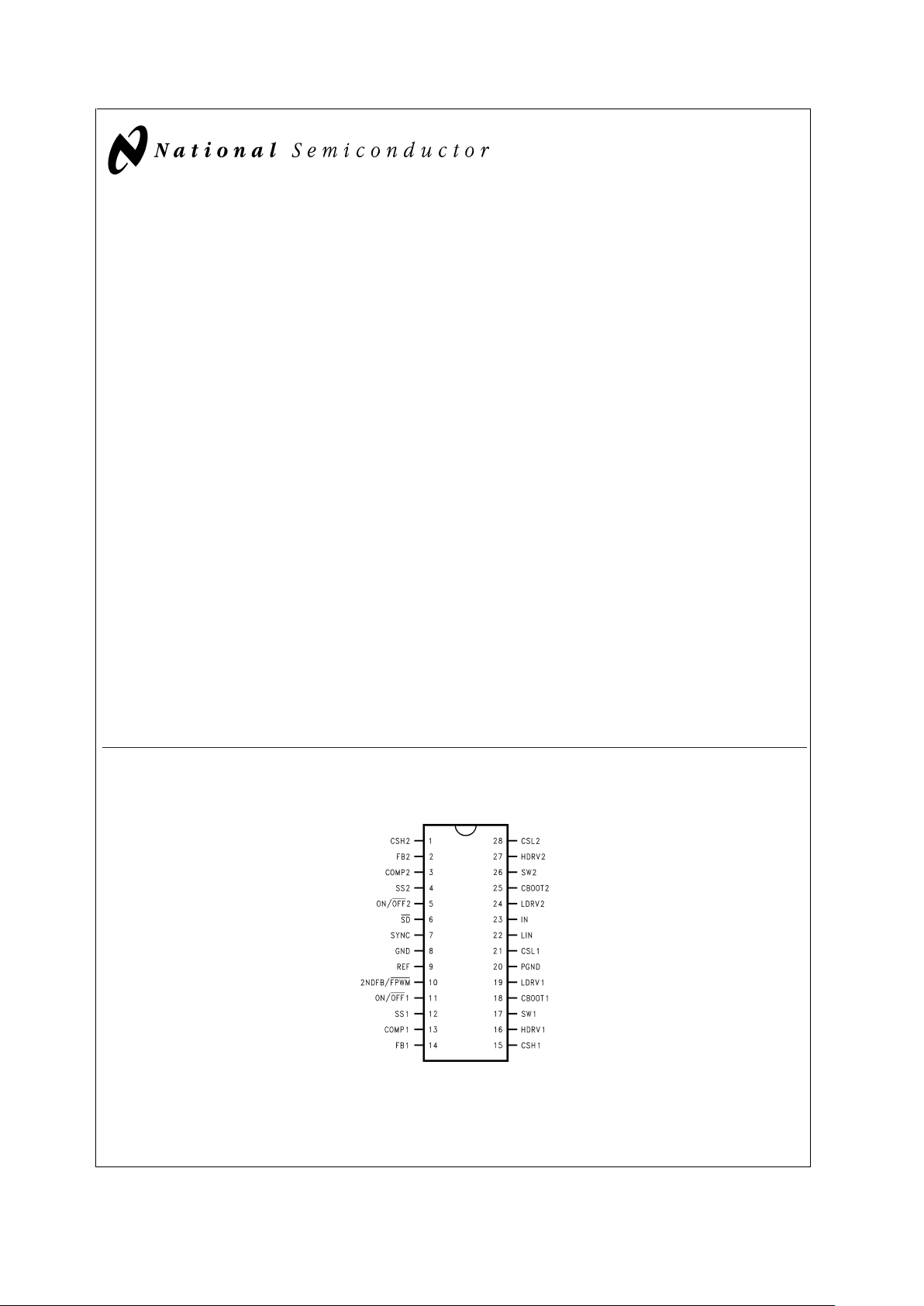
Connection Diagram and Ordering Information
28-Lead TSSOP (MTC)
DS100949-1
Top View
Order Number LM2641MTC-ADJ
See NS Package Number MTC28
January 2000
LM2641 Dual Adjustable Step-Down Switching Power Supply Controller
© 2000 National Semiconductor Corporation DS100949 www.national.com
Page 2
Pin Description (Refer to Typical Application Circuits)
Pin
#
Name Function
1 CSH2 The sense point for the positive side of the voltage across the current sense resistor (R13)
placed in series with output
#
2.
2 FB2 The regulated output voltage appearing at output
#
2 is sensed using this pin by connecting it to
the center of the output resistive divider (R15 and R16).
3 COMP2 An R-C network made up of R11, C10, and C12 is connected to this pin which provides loop
compensation for regulated output
#
2.
4 SS2 This provides programmable soft-start for the
#
2 output along with capacitor C15.
5 ON/OFF2
This pin turns off only output#2.
6SD
The part can be put into “sleep” mode using this pin, where both outputs are off and the internal
chip functions are shut down.
7 SYNC The internal oscillator may be synchronized to an external clock via this pin.
8 GND Connect this pin to circuit Signal Ground.
9 REF Internal 2.5V reference voltage. This voltage is turned off by the SD pin, but remains on if either
or both ON/OFF pins are pulled low, which turns off the regulated output(s).
10 2NDFB/FPWM A 12V supply can be generated using an auxiliary winding on the 5V output inductor. Feedback
to control this 12V output is brought in through this pin. If the 12V supply is not required, this
pin can also force the chip to operate at fixed frequency at light loads by pulling the pin low
(this is the “forced-PWM” mode of operation). This will prevent the converter from operating in
pulse-skipping mode.
11 ON/OFF1
This pin turns off only output#1.
12 SS1 This provides programmable soft-start for the
#
1 output along with capacitor C3.
13 COMP1 An R-C network made up of R6, C5, and C7 is connected to this pin which provides loop
compensation for regulated output
#
1.
14 FB1 The regulated output voltage appearing at output
#
1 is sensed using this pin by connecting it to
the center of the output resistive divider (R1 and R2).
15 CSH1 The sense point for the positive side of the voltage across the current sense resistor (R4)
placed in series with output
#
1.
16 HDRV1 The drive for the gate of the high-side switching FET used for output
#
1.
17 SW1 This is the switching output drive point of the two power FETs which produce output
#
1.
18 CBOOT1 The bootstrap capacitor (C8) for output
#
1 is returned to this point.
19 LDRV1 The drive for the gate of the low-side switching FET (synchronous rectifier) used for output
#
1.
20 PGND Connect this pin to circuit Power Ground.
21 CSL1 The sense point for the negative side of the voltage across the current sense resistor (R4)
placed in series with output
#
1.
22 LIN This pin provides a low-current (50 mA max) 5V output. This output is always on, and can not
be turned off by either the SD or ON/OFF pins.
23 IN This is the connection for the main input power.
24 LDRV2 The drive for the gate of the low-side switching FET (synchronous rectifier) used for output
#
2.
25 CBOOT2 The bootstrap capacitor (C9) for output
#
2 is returned to this point.
26 SW2 This is the switching output drive point of the two power FETs which produce output
#
2.
27 HDRV2 The drive for the gate of the high-side switching FET used for output
#
2.
28 CSL2 The sense point for the negative side of the voltage across the current sense resistor (R13)
placed in series with output
#
2.
LM2641
www.national.com 2
Page 3
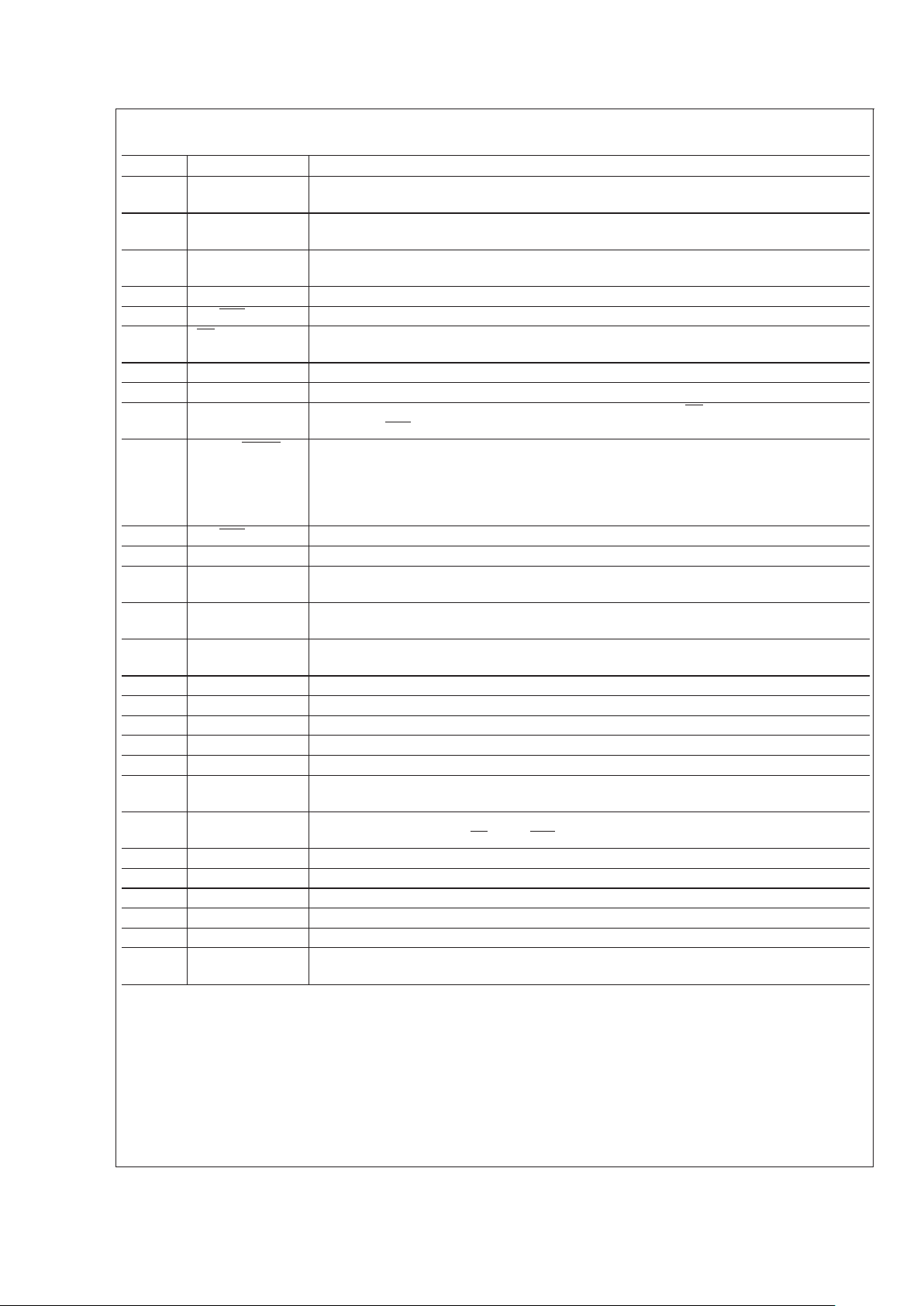
Typical Application Circuits
DS100949-3
FIGURE 1. Application With 5V/3A and 3.3V/4A Outputs
LM2641
www.national.com3
Page 4
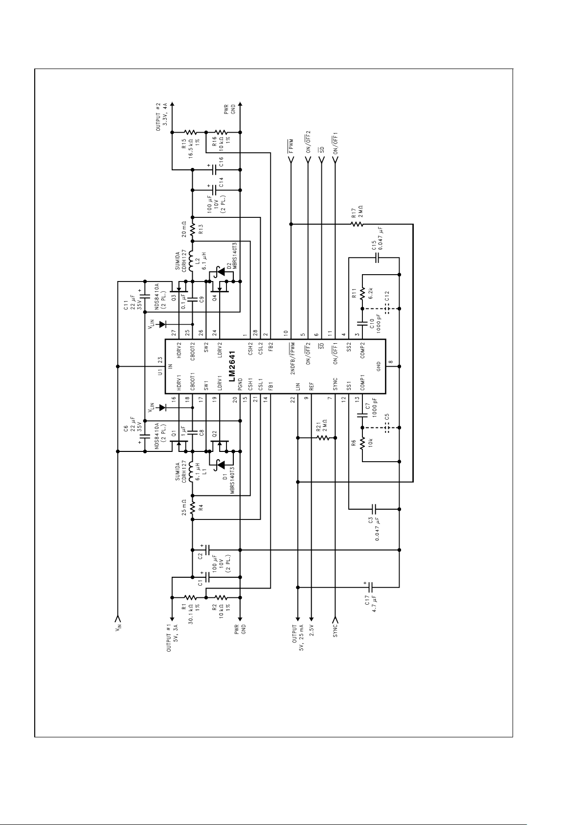
Typical Application Circuits (Continued)
DS100949-4
FIGURE 2. Application With 5V/3A, 3.3V/4A, and 12V/0.3A Outputs
LM2641
www.national.com 4
Page 5
Absolute Maximum Ratings (Notes 2, 1)
If Military/Aerospace specified devices are required,
please contact the National Semiconductor Sales Office/
Distributors for availability and specifications.
IN, SW1, and SW2 −0.3 to 31V
FB1 and FB2 −0.3 to 3V
SD, ON/OFF1, ON/OFF2,
2NDFB/FPWM, SYNC, REF,
SS1, SS2, COMP1,
COMP2 and CSL1
−0.3 to (V
LIN
+0.3)V
LIN −0.3 to 6V
CSH1, CSH2, and CSL2 (Note
12)
−0.3 to 9V
Voltage from CBOOT1 to SW1
and from CBOOT2 to SW2
−0.3 to 5V
Voltage from HDRV1 to SW1
and from HDRV2 to SW2
−0.3V
Voltage from CBOOT1 to
HDRV1 and from CBOOT2
HDRV2
−0.3V
Junction Temp. +150˚C
Power Dissipation (Note 3) 883 mW
Ambient Storage Temp. (T
J
) −65 to +150˚C
Soldering Dwell Time, Temp. (Note 4)
Wave 4 sec, 260˚C
Infrared 10 sec, 240˚C
Vapor Phase 75 sec, 219˚C
ESD Rating (Note 5) 2 kV
Operating Ratings (Notes 1, 2)
V
IN
5.5 to 30V
Junction Temp. (T
J
) 0 to +125˚C
Electrical Characteristics
Typicals and limits appearing in regular type apply for T
J
=
25˚C. Limits appearing in boldface type apply over the entire junc-
tion temperature range for operation, 0 to +125˚C. Unless otherwise specified under the Parameter or Conditions columns, V
IN
=
10V, and V
SD
=
V
ON/OFF1
=
V
ON/OFF2
=
5V. (Notes 2, 6, 7)
Symbol Parameter Conditions Typical Limit Units
System
V
IN
Input Supply Voltage Range 5.5 V(min)
30 V(max)
V
OUT1
Output Voltage Adjustment
Range
2.2 V(min)
6.0 V(max)
V
OUT2
Output Voltage Adjustment
Range
2.2 V(min)
8.0 V(max)
∆V
OUT/VOUT
Load Regulation 0 mV ≤ (CSH1-CSL1) ≤ 80 mV,
0mV≤(CSH2-CSL2) ≤ 80 mV
0.5
%
∆V
OUT
/∆V
IN
Line Regulation 5.5V ≤ VIN≤ 30V 0.002
%
/V
I
IN
Input Supply Current ON (Note 8) 0.6 mA
V
FB1
=
V
FB2
=
1.4V, 1 mA(max)
V
CSH1
=
5.2V, V
CSL1
=
5V,
V
CSH2
=
3.5V, V
CSL2
=
3.3V
Standing By (Note 9) 80 µA
V
ON/OFF1
=
V
ON/OFF2
=
0V
150 µA(max)
Shut Down (Note 10) 25 µA
V
SD
=
0V
60 µA(max)
I
SS1,ISS2
Soft-Start Source Current V
SS1
=
V
SS2
=
1V 4.75 µA
2.0 µA(min)
7.0 µA(max)
Soft-Start Sink Current 10 µA
V
PCL
Positive Current Limit
Voltage (Voltage from CSH1
to CSL1 and from CSH2 to
CSL2)
100 mV
80
mV(min)
140 mV(max)
V
NCL
Negative Current Limit
Voltage (Voltage from CSH1
to CSL1 and from CSH2 to
CSL2)
V
2NDFB/FPWM
=
0.8V
−100 mV
−80 mV(min)
−140 mV(max)
LM2641
www.national.com5
Page 6
Electrical Characteristics (Continued)
Typicals and limits appearing in regular type apply for T
J
=
25˚C. Limits appearing in boldface type apply over the entire junc-
tion temperature range for operation, 0 to +125˚C. Unless otherwise specified under the Parameter or Conditions columns, V
IN
=
10V, and V
SD
=
V
ON/OFF1
=
V
ON/OFF2
=
5V. (Notes 2, 6, 7)
Symbol Parameter Conditions Typical Limit Units
System
V
OUT
Undervoltage
Shutdown Latch Threshold
70
%
60
%
(min)
80
%
(max)
V
OUT
Overvoltage Shutdown
Latch Threshold
150
%
135
%
(min)
165
%
(max)
Secondary Feedback
Threshold Voltage
(2NDFB/FPWM)
2.5 V
2.4 V(min)
2.6 V(max)
(2NDFB/FPWM) Pin
Pull-Up Current
V
SFB
=
2.4V
V
ON/OFF1
=
0V
V
ON/OFF2
=
5V
40 80 µA(max)
(2NDFB/FPWM) Pin
Input Leakage Current
±
0.1 µA
Gate Drive
V
BOOT
Bootstrap Voltage (Voltage
from CBOOT1 to SW1 and
from CBOOT2 to SW2)
CBOOT1 and CBOOT2 Source
1µA Each
4.5 V
4.3 V(min)
HDRV1 and HDRV2 Sink
and Source Current
0.35 A
LDRV1 and LDRV2 Sink and
Source Current
0.35 A
HDRV1 and HDRV2
High-Side On-Resistance
V
CBOOT1
=
V
CBOOT2
=
5V, V
SW1
=
V
SW2
=
0V
6 Ω
HDRV1 and HDRV2
Low-Side On-Resistance
V
CBOOT1
=
V
CBOOT2
=
5V, V
SW1
=
V
SW2
=
0V
4 Ω
LDRV1 and LDRV2
High-Side On-Resistance
V
LIN
=
5V 8 Ω
LDRV1 and LDRV2 Low-Side
On-Resistance
V
LIN
=
5V 4 Ω
Oscillator
F
OSC
Oscillator Frequency 300 kHz
255 kHz(min)
345 kHz(max)
Minimum OFF-Time V
FB1
=
1V, Measured at HDRV1 250 ns
350 ns(max)
Maximum Frequency of
Synchronization
400 kHz(min)
Minimum Width of
Synchronization Pulses
SYNC Pulses are Low-Going 200 ns(min)
Error Amplifier
I
FB1,IFB2
Feedback Input Bias Current V
FB1
=
V
FB2
=
1.4V 100 nA
250 nA(max)
I
COMP1,ICOMP2
COMP Output Source
Current
V
FB1
=
V
FB2
=
1V, V
COMP1
=
V
COMP2
=
1V
90 µA
40 µA(min)
I
COMP1,ICOMP2
COMP Output Sink Current V
FB1
=
V
FB2
=
1.4V, V
COMP1
=
V
COMP2
=
0.2V
60 µA
40 µA(min)
LM2641
www.national.com 6
Page 7

Electrical Characteristics (Continued)
Typicals and limits appearing in regular type apply for T
J
=
25˚C. Limits appearing in boldface type apply over the entire junc-
tion temperature range for operation, 0 to +125˚C. Unless otherwise specified under the Parameter or Conditions columns, V
IN
=
10V, and V
SD
=
V
ON/OFF1
=
V
ON/OFF2
=
5V. (Notes 2, 6, 7)
Symbol Parameter Conditions Typical Limit Units
Voltage References and Linear Voltage Regulator
V
BG
Bandgap Voltage 1.238 V
V
REF
Reference Voltage 0.01 mA ≤ I
REF
≤ 5 mA Source,
V
LIN
≤ 6V
2.5 V
2.45 V(min)
2.55 V(max)
V
LIN
Output Voltage of the Linear
Voltage Regulator
6V ≤ VIN≤ 30V,
0mA≤I
LIN
≤ 25 mA
5V
4.6 V(min)
5.4 V(max)
V
UVLO
Undervoltage Lockout
Threshold
(Note 11) 4.0 V
3.6 V(min)
4.4 V(max)
LIN-to-V
OUT
Switch-Over
Threshold
V
OUT
taken at CSL1 4.8 V
Logic Inputs
V
IH
Minimum High Level Input
Voltage (SD, ON/OFF1,
ON/OFF2, and SYNC)
2.4 V(min)
V
IH
Minimum High Level Input
Voltage (2NDFB/FPWM)
2.6 V(min)
V
IL
Maximum Low Level Input
Voltage (SD, ON/OFF1,
ON/OFF2, SYNC, and
2NDFB/FPWM)
0.8 V(max)
Maximum Input Leakage
Current (SD, ON/OFF1,
ON/OFF2, and SYNC)
Logic Input Voltage 0 or 5V
±
0.1 µA
Note 1: Unless otherwise specified, all voltages are with respect to the voltage at the GND and PGND pins.
Note 2: Absolute Maximum Ratings are limits beyond which damage to the device may occur. Operating Ratings are conditions under which operation of the device
is guaranteed. Operating Ratings do not imply guaranteed performance limits. For guaranteed performance limits and associated test conditions, see the Electrical
Characteristics tables.
Note 3: The Absolute Maximum power dissipation depends on the ambient temperature. The 883 mW rating results from substituting 150˚C, 70˚C, and 90.6˚C/W
for T
Jmax,TA
, and θJArespectively into the formula P
max
=
(T
Jmax-TA
)/θJA, where P
max
is theAbsoluteMaximumpowerdissipation,T
Jmax
is theAbsoluteMaximum
junction temperature, T
A
is the ambient temperature, and θJAis the junction-to-ambient thermal resistance of the package. A θJAof 90.6˚C/W represents the
worst-case condition of no heat sinking of the 28-pin TSSOP.Heat sinking allows the safe dissipation of more power. TheAbsoluteMaximumpowerdissipationmust
be derated by 11.04 mW per ˚C above 70˚C ambient. The LM2641 actively limits its junction temperature to about 150˚C.
Note 4: For detailed information on soldering plastic small-outline packages, refer to the Packaging Databook available from National Semiconductor Corporation.
Note 5: For testing purposes, ESD was applied using the human-body model, a 100 pF capacitor discharged through a 1.5 kΩ resistor.
Note 6: A typical is the center of characterization data taken with T
A
=
T
J
=
25˚C. Typicals are not guaranteed.
Note 7: All limits are guaranteed. All electrical characteristics having room-temperature limits are tested during production with T
A
=
25˚C. All hot and cold limits are
guaranteed by correlating the electrical characteristics to process and temperature variations and applying statistical process control.
Note 8: Both controllers are ON but not switching. Currents entering the IC at IN, CSL1, CSH1, CSL2, and CSH2 are measured. Those entering at CSL1 and CSH1
are multiplied by 0.50 to emulate the effect of a switching conversion from 10V down to 5V.Those entering at CSL2 and CSH2 are multiplied by 0.33 to emulate the
effect of a switching conversion from 10V down to 3.3V. After multiplication, all five currents are added. Because the voltage at the CSL1 input is greater than the
LIN-to-V
OUT
switchover threshold, most of the input supply current enters the IC via the CSL1 input.
Note 9: Both switching controllers are OFF. The 5V, 50 mA linear regulator (output at LIN) and the precision 2.5V reference (output at REF) remain ON.
Note 10: Both switching controllers and the 2.5V precision reference are OFF.The 5V, 50 mA linear regulator remains ON.
Note 11: The controllers remain OFF until the voltage of the 5V, 50 mA linear regulator (output at LIN) reaches this threshold.
Note 12: In applications where the output voltage can exceed the absolute maximum rating, a 100Ω resistor must be placed in series with the CSH and CSL inputs.
LM2641
www.national.com7
Page 8

Block Diagram
DS100949-2
FIGURE 3. LM2641 Block Diagram
LM2641
www.national.com 8
Page 9

Typical Performance Charateristics
Efficiency vs Load Current
DS100949-14
Efficiency vs Load Current
DS100949-15
Efficiency vs Load Current
DS100949-16
Efficiency vs Load Current
DS100949-17
Efficiency vs Load Current
DS100949-18
Efficiency vs Load Current
DS100949-19
Efficiency vs Load Current
DS100949-20
Efficiency vs Load Current
DS100949-21
Efficiency vs Load Current
DS100949-22
Ref Output Voltage
DS100949-23
Ref Output Voltage
DS100949-24
Normalized Switching Output
Voltage vs
Junction Temperature
DS100949-25
LM2641
www.national.com9
Page 10

Typical Performance Charateristics (Continued)
Theory of Operation
Basic Operation of the Current-Mode Controller
The output voltage is held at a constant value by the main
control loop, which is made up of the
error amplifier
, the
cur-
rent sense amplifier
, and the
PWM comparator
(refer to the
Block Diagram,
Figure 3
).
The LM2641 controller has two primary modes of operation:
Forced Pulse-Width Modulation (FPWM)
where the control-
ler always operates at a fixed frequency, and
Pulse-Skipping
mode where the controller frequency decreases at reduced
output loads to improve light-load efficiency.
FPWM Mode of Operation
Pulling the FPWM pin low initiates a mode of operation
called Forced Pulse-Width Modulation (FPWM). This means
that the LM2641 will
always
operate at a fixed frequency, re-
gardless of output load. The cycle of operation is:
The high-side FET switch turns ON at the beginning of every
clock cycle, causing current to flow through the inductor. The
inductor current ramps up, causing a voltage drop across the
sense resistor, and this voltage is amplified by the current
sense amplifier.
The voltage signal from the current sense amplifier is applied
to the input of the PWM comparator, where it is compared to
the control level set by the error amplifier. Once the current
sense signal reaches this control voltage, the PWM comparator resets the driver logic which turns OFF the high-side
FET switch.
The low-side FET switch turns on after a delay time which is
the lesser of either:
(a) The time it takes the SW pin voltage to reach zero (this
voltage is sensed by the shoot-through protection circuitry).
(b) 100 ns, which is the pre-set value for maximum delay.
When operating at very light loads (in FPWM mode), the inductor current must flow in a negative direction through the
low-side FET switch in order to maintain the fixed-frequency
mode of operation. For this reason, the built-in zero cross
detector is disabled when ever FPWM mode is activated
(that is, when ever the FPWM pin is pulled to a low state).
It should be noted that if the FPWM pin is high (operation described in next section), the zero cross detector will turn OFF
the low-side FET switch anytime the inductor current drops
to zero (which prevents negative inductor current).
Pulse-Skipping Mode of Operation
Pulling the FPWM pin high allows the LM2641 to operate in
pulse-skipping mode at light loads, where the switching frequency decreases as the output load is reduced. The controller will operate in fixed-frequency mode, as described in
the previous section, if the output load current is sufficiently
high.
Pulse-skipping results in higher efficiency at light loads, as
decreasing the switching frequency reduces switching
Normalized Error Amplifier Voltage
vs
Junction Temperature
DS100949-26
Error Amplifier Gm vs
Junction Temperature
DS100949-27
Normalized Oscillator Frequency
vs
Junction Temperature
DS100949-28
Shutdown Quiescent Current
And Standby Quiescent Current vs
Supply Voltage
DS100949-29
LM2641
www.national.com 10
Page 11

Theory of Operation (Continued)
losses. The load current value where the transition from
fixed-frequency to pulse-skipping operation occurs is the
point where the inductor current goes low enough to cause
the voltage measured across the current sense resistor (R4
or R13) to drop below 25 mV.
In pulse-skipping mode, the high-side FET switch will turn
ON at the beginning of the first clock cycle which occurs after
the voltage at the feedback pin falls below the reference voltage. The high-side FET switch remains ON until the voltage
across the current sense resistor rises to 25 mV (and then it
turns OFF).
Ramp Compensation
All current-mode controllers require the use of ramp compensation to prevent subharmonic oscillations, and this compensation is built into the LM2641. The internal compensation assumes an R
SENSE
value of 25 mΩ, inductor value of
6.8µH, and a maximum output voltage of 6V.
To prevent oscillations, the slope M of the compensation
ramp must be equal to the maximum downward slope of the
voltage waveform at the output of the current sense amplifier. The relationship of the slope M to the external components is given by:
M
COMP
=
M
CS AMP
(max)=NXR
SENSE
XV
OUT
(max) / L
Where:
M
COMP
is the slope of the compensation ramp.
M
CS AMP
(max) is the maximum downward slope of the volt-
age at the output of the current sense amplifier.
N is the gain of the current sense amplifier.
R
SENSE
is the value of the current sense resistor.
V
OUT
(max) is the maximum output voltage.
L is the inductance of the output inductor.
It is important to note that since the value R
SENSE
appears in
the numerator and L is in the denominator, these two values
may be increased or decreased at the same ratio without
changing the slope.
At higher values of load current, a lower value R
SENSE
will be
selected. The inductance value for the output inductor
should be decreased by the same percentage to maintain
correct ramp compensation.
Application Information
Improved Transient Response
If the output voltage falls below 97%of the nominal value,
the low-voltage regulation (LREG) comparator will activate
logic which turns ON the high-side FET switch continuously
until the output returns to nominal. The low-side FET switch
is held OFF during this time.
This action will improve transient response since it bypasses
the error amplifier and PWM comparator, forcing the
high-side switch ON until the output returns to nominal. This
feature is disabled during start-up.
Boost High-Side Gate Drive
A “flying” bootstrap capacitor is used to generate the gate
drive voltage used for the high-side FET switch. This bootstrap capacitor is charged up to about 5V using an internal
supply rail and diode when ever the low-side FET switch is
ON. When the high-side FET switch turns ON, the Source is
pulled up near the input voltage. The voltage across the
bootstrap capacitor boosts up the gate drive voltage, ensuring that the Gate is driven at least 4.3V higher than the
Source.
Reference
The internal bandgap reference is used to generate a 2.5V
reference voltage which is connected to the REF pin. The
guaranteed tolerance of the REF voltage is
±
2%over the full
operating temperature range, as long as the current drawn is
≤ 5 mA.
A bypass capacitor on the REF pin is not required, but may
be used to reduce noise.
5V LIN Output
The LM2641 contains a built-in 5V/50 mA LDO regulator
whose output is connected to the LIN pin. Since this is an
LDO regulator, it does require an external capacitor to maintain stability. A good quality Tantalum capacitor ≥ 4.7µF is
recommended.
Since the current limit for this LDO regulator is set at about
85 mA, it can be used at load currents up to about 50 mA
(assuming total IC power dissipation does not exceed the
maximum value).
Guaranteed specifications are provided for worst-case values of V
LIN
over the full operating temperature range for load
currents up to 25mA (see Electrical Characteristics). To estimate how the V
LIN
output voltage changes when going from
I
LIN
=
25mA to I
LIN
=
50mA, a change in V
LIN
of about
−30mV should be expected due to loading (typical value
only,not guaranteed). This decrease in V
LIN
is linear with in-
creasing load current.
It must be understood that the maximum allowable current of
50mA must include the current drawn by the gate drive circuitry. This means that the maximum current available for
use at the LIN pin is 50 mA minus whatever is being used internally for gate drive.
The amount of current used for gate drive by each switching
output can be calculated using the formula:
I
GD
=2XQXF
OSC
Where:
I
GD
is the gate drive current supplied by V
LIN
.
Q is the gate charge required by the selected FET (see FET
data sheet: Gate Charge Characteristics).
F
OSC
is the switching frequency.
Example: As shown in the typical application, if the FET
NDS8410 is used with the LM2641, the turn-on gate voltage
(V
GS
)is5V−V
DIODE
=
4.3V. Referring to the NDS8410 data
sheet, the curve Gate Charge Characteristics shows that the
gate charge for this value of V
GS
is about 24 nC.
Assuming 300 kHz switching frequency, the gate drive current used by each switching output is:
I
GD
=
2XQXF
OSC
=
2X(24X10
−9
)X(3X10⁵)
=
14.4 mA
If both outputs are switching, the total gate drive current
drawn would be twice (28.8 mA).
Note that in cases where the voltage at switching output
#
1
is 4.8V or higher, the internal gate drive current is obtained
from that output (which means the full 50 mA is available for
external use at the LIN pin).
LM2641
www.national.com11
Page 12

Application Information (Continued)
SYNC Pin
The basic operating frequency of 300kHz can be increased
to up to 400kHz by using the SYNC pin and an external
CMOS or TTL clock. The synchronizing pulses must have a
minimum pulse width of 200 ns.
If the sync function is not used, the SYNC pin must be connected to the LIN pin or to ground to prevent false triggering.
Current Limit Circuitry
The LM2641 is protected from damage due to excessive output current by an internal current limit comparator, which
monitors output current on a cycle-by-cycle basis. The current limiter activates when ever the absolute magnitude of
the voltage developed across the output sense resistor exceeds 100 mV (positive or negative value).
If the sensed voltage exceeds 100 mV, the high-side FET
switch is turned OFF. If the sensed voltage goes below -100
mV, the low-side FET switch is turned OFF. It should be
noted that drawing sufficient output current to activate the
current limit circuits can cause the output voltage to drop,
which could result in a under-voltage latch-OFF condition
(see next section).
Under-voltage/Over-voltage Protection
The LM2641 contains protection circuitry which activates if
the output voltage is too low (UV) or too high (OV). In the
event of either a UV or OV fault, the LM2641 is latched off
and the high-side FET is turned off, while the low-side FET is
turned on.
If the output voltage drops below 70%of nominal value, the
under-voltage comparator will latch OFF the LM2641. To restore operation, power to the device must be shut off and
then restored.
It should be noted that the UV latch provides protection in
cases where excessive output current forces the output voltage down. The UV latch circuitry is disabled during start-up.
If the output voltage exceeds 150%of nominal, the
over-voltage comparator latches off the LM2641. As stated
before, power must be cycled OFF and then ON to restore
operation.
It must be noted that the OV latch can not protect the load
from damage in the event of a high-side FET switch failure
(where the FET shorts out and connects the input voltage to
the load).
Protection for the load in the event of such a failure can be
implemented using a fuse in the power lead. Since the
low-side FET switch turns ON whenever the OV latch activates, this would blow a series fuse if the FET and fuse are
correctly sized.
Soft-Start
An internal 5 µA current source connected to the soft-start
pins allows the user to program the turn-on time of the
LM2641. If a capacitor is connected to the SS pin, the voltage at that pin will ramp up linearly at turn ON. This voltage
is used to control the pulse widths of the FET switches.
The pulse widths start at a very narrow value and linearly increase up to the point where the SS pin voltage is about
1.3V. At that time, the pulse-to-pulse current limiter controls
the pulse widths until the output reaches its nominal value
(and the PWM current-mode control loop takes over).
The LM2641 contains a digital counter (referenced to the oscillator frequency) that times the soft-start interval. The maximum allotted SS time period is 4096 counts of the oscillator
clock, which means the time period varies with oscillator frequency:
max. allowable SS interval=4096 / F
OSC
If the output voltage does not move to within −1%of nominal
in the period of 4096 counts, the device will latch OFF.To restore operation, the power must be cycled OFF to ON.
Minimum Pulse Width
As the input voltage is increased, the pulse widths of the
switching FET’s decreases. If the pulse widths become narrower than 350ns, pulse jitter may occur as the pulses alternate with slightly different pulse widths. This is does not affect regulator stability or output voltage accuracy.
Loop Compensation
The LM2641 must be properly compensated to assure
stable operation and good transient response. As with any
control loop, best performance is achieved when the compensation is optimized so that maximum bandwidth is obtained while still maintaining sufficient phase margin for good
stability.
Best performance for the LM2641 is typically obtained when
the loop bandwidth (defined as the frequency where the loop
gain equals unity) is in the range of F
OSC
/10 to F
OSC
/5.
In the discussion of loop stability, it should be noted that
there is a high-frequency pole f
p
(HF), whose frequency can
be approximated by:
f
p
(HF) ∼ F
OSC
/2XQS(Assumes Q
S
<
0.5)
Where:
As can be seen in the approximation for QS, the highest frequency for f
p
(HF) occurs at the maximum value of VIN. The
lowest frequency for f
p
(HF) is about F
OSC
/10 (when V
IN
=
4.5V and V
OUT
=
1.8V).
As noted above, the location of the pole f
p
(HF) is typically in
the range of about F
OSC
/10 to F
OSC
/4. This pole will often be
near the unity-gain crossover frequency, and it can significantly reduce phase margin if left uncompensated. Fortunately,the ESR of the output capacitor(s) forms a zero which
is usually very near the frequency of f
p
(HF), and provides
cancellation of the negative phase shift it would otherwise
cause. For this reason, the output capacitor must be carefully selected.
Most of the loop compensation for the LM2641 is set by an
R-C network from the output of the error amplifier to ground
(see
Figure 4
). Since this is a transconductance amplifier, it
has a very high output impedance (160 kΩ).
LM2641
www.national.com 12
Page 13

Application Information (Continued)
The components shown will add poles and zeros to the loop
gain as given by the following equations:
C10 adds a pole whose frequency is given by:
f
p
(C10)=1/[2πX C10 (R11 + 160k) ]
C12 adds a pole whose frequency is given by:
f
p
(C12)=1/[2πX C12 (R11 || 160k) ]
R11 adds a zero whose frequency is given by:
f
z
(R11)=1/[2πX R11 (C10 + C12) ]
The output capacitor adds both a pole and a zero to the loop:
f
p(COUT
)=1/[2πXRLXC
OUT
]
f
z
(ESR)=1/[2πXESRXC
OUT
]
Where R
L
is the load resistance, and ESR is the equivalent
series resistance of the output capacitor(s).
The function of the compensation components will be ex-
plained in a qualitative discussion of a typical loop gain plot
for an LM2641 application, as illustrated in
Figure 5
.
C10 and R11 form a pole and a zero. Changing the value of
C10 moves the frequency of both the pole and the zero.
Changing R11 moves the zero without significantly affecting
the pole.
The C10 pole is typically referred to as the dominant pole,
and its primary function is to roll off loop gain and reduce the
bandwidth.
The R11 zero is required to add some positive phase shift to
offset some of the negative phase shift from the two
low-frequency poles. Without this zero, these two poles
would cause −180˚ of phase shift at the unity-gain crossover,
which is clearly unstable. Best results are typically obtained
if R11 is selected such that the frequency of f
z
(R11) is in the
range of f
c
/4 to fcwhere fcis the unity-gain crossover fre-
quency.
The output capacitor (along with the load resistance R
L
)
forms a pole shown as f
p(COUT
). Although the frequency of
this pole varies with R
L
, the loop gain also varies proportionally which means the unity-gain crossover frequency stays
essentially constant regardless of R
L
value.
C12 can be used to create an additional pole most often
used for bypassing high-frequency switching noise on the
COMP pin. In many applications, this capacitor is unnecessary.
If C12 is used, best results are obtained if the frequency of
the pole is set in the range F
OSC
/2 to 2F
OSC
. This will provide
bypassing for the high-frequency noise caused by switching
transitions, but add only a small amount of negative phase
shift at the unity-gain crossover frequency.
The ESR of C
OUT
(as well as the capacitance of C
OUT
) form
the zero f
z
(ESR), which typically falls somewhere between
10kHz and 50kHz. This zero is very important, as it cancels
phase shift caused by the high-frequency pole f
p
(HF). It is
important to select C
OUT
with the correct value of capaci-
tance and ESR to place this zero near f
c
(typical range fc/2 to
f
c
).
As an example, we will present an analysis of the loop gain
plot for a 3.3V design. Values used for calculations are:
V
IN
=
12V
V
OUT
=
3.3V
@
4A
C
OUT
=
C14 + C16=200 µF
ESR=60 mΩ(each)=30mΩ total
F
OSC
=
300kHz
f
p
(HF) ∼ 40kHz
R13=20mΩ
L2=6.8 µH
R
L
=
0.825Ω
DC gain=55dB
The values of compensation components will be: C10
=
2200 pF, R11=8.2k, and C12 will not be used. Using this
data, the poles and zeros are calculated:
f
p
(C10)=1/[2πX C10 (R11 + 160k) ]=430Hz
f
z
(R11)=1/[2πX R11 (C10 + C12) ]=8.8kHz
f
p(COUT
)=1/[2πXRLXC
OUT
]=960Hz
f
z
(ESR)=1/[2πXESRXC
OUT
]=27kHz
f
p
(HF) ∼ 40kHz
Using these values, the calculated gain plot is shown in
Fig-
ure 6
.
DS100949-5
FIGURE 4. Typical Compensation Network
DS100949-6
FIGURE 5. Typical Loop Gain Plot
LM2641
www.national.com13
Page 14

Application Information (Continued)
Looking at the plot, it can be seen that the unity-gain crossover frequency f
c
is expected to be about 25kHz. Using this
value, the phase margin at the point is calculated to be about
84˚.
To verify the accuracy of these calculations, the circuit was
bench tested using a network analyzer. The measured gain
and phase are shown plotted in
Figure 7
.
The measured gain plot agrees very closely to the predicted
values. The phase margin at 0dB is slightly less than predicted (71˚ vs. 84˚), which is to be expected due to the negative phase shift contributions of high frequency poles not included in this simplified analysis.
It should be noted that 70˚ phase margin with 25kHz bandwidth is excellent, and represents the optimal compensation
for this set of values for V
IN,VOUT
, inductor and RL.
Optimizing Stability
The best tool for measuring both bandwidth and phase margin is a network analyzer. If this is not available, a simple
method which gives a good measure of loop stability is to apply a minimum to maximum step of output load current and
observe the resulting output voltage transient. A design
which has good phase margin (
>
50˚) will typically show no
ringing after the output voltage transient returns to its nominal value.
It should be noted that the stability (phase margin) does not
have to be optimal for the regulator to be stable. The design
analyzed in the previous section was re-compensated by
changing R11 and C10 to intentionally reduce the phase
margin to about 35˚ and re-tested for step response. The
output waveform displayed slight ringing after the initial return to nominal, but was completely stable otherwise.
In most cases, the compensation components shown in the
Typical Application Circuits will give good performance. To
assist in optimizing phase margin, the following guidelines
show the effects of changing various components.
C
OUT
: Increasing the capacitance of C
OUT
moves the fre-
quency of the pole f
p(COUT
) to a lower value and reduces
loop bandwidth. Increasing C
OUT
can be beneficial (increasing the phase margin) if the loop bandwidth is too wide
(
>
F
OSC
/5) which places the high-frequency poles too close
to the unity-gain crossover frequency.
ESR of C
OUT
: The ESR forms a zero fz(ESR), which is
needed to cancel negative phase shift near the unity-gain
frequency. High-ESR capacitors can not be used, since the
zero will be too low in frequency which will make the loop
bandwidth too wide.
R11/C10:These form a pole and a zero. Changing the value
of C10 changes the frequency of both the pole and zero.
Note that since this causes the frequency of both the pole
and zero to move up or down together, adjusting the value of
C10 does not significantly affect loop bandwidth.
Changing the value of R11 moves the frequency location of
the zero f
z
(R11),but does not significantly shift the C10 pole
(since the value of R11 is much less than the 160kΩ output
impedance of the Gm amplifier). Since only the zero is
moved, this affects both bandwidth and phase margin. This
means adjusting R11 is an easy way to maximize the positive phase shift provided by the zero. Best results are typically obtained if f
z
(R11) is in the frequency range of fc/4 to f
c
(where fcis the unity-gain crossover frequency).
Design Procedure
This section presents guidelines for selecting external components.
INDUCTOR SELECTION
In selecting an inductor, the parameters which are most important are inductance, current rating, and DC resistance.
Inductance
It is important to understand that all inductors are not created
equal, as the method of specifying inductance varies widely.
It must also be noted that the inductance of every inductor
decreases with current. The core material, size, and construction type all contribute the the inductor’s dependence
on current loading. Some inductors exhibit inductance
curves which are relatively flat, while others may vary more
than 2:1 from minimum to maximum current. In the latter
case, the manufacturer’s specified inductance value is usually the maximum value, which means the actual inductance
in your application will be much less.
An inductor with a flatter inductance curve is preferable,
since the loop characteristics of any switching converter are
affected somewhat by inductance value. An inductor which
has a more constant inductance value will give more consistent loop bandwidth when the load current is varied.
DS100949-7
FIGURE 6. Calculated Gain Plot for 3.3V/4A Application
DS100949-8
FIGURE 7. Measured Gain/Phase Plot for 3.3V/4A
Application
LM2641
www.national.com 14
Page 15

Design Procedure (Continued)
The data sheet for the inductor must be reviewed carefully to
verify that the selected component will have the desired inductance at the frequency and current for the application.
Current Rating
This specification may be the most confusing of all when
picking an inductor, as manufacturers use different methods
for specifying an inductor’s current rating.
The current rating specified for an inductor is typically given
in RMS current, although in some cases a peak current rating will also be given (usually as a multiple of the RMS rating) which gives the user some indication of how well the inductance operates in the saturation region.
Other things being equal, a higher peak current rating is preferred, as this allows the inductor to tolerate high values of
ripple current without significant loss of inductance.
In the some cases where the inductance vs. current curve is
relatively flat, the given current rating is the point where the
inductance drops 10%below the nominal value. If the inductance varies a lot with current, the current rating listed by the
manufacturer may be the “center point” of the curve. This
means if that value of current is used in your application, the
amount of inductance will be less than the specified value.
DC Resistance
The DC resistance of the wire used in an inductor dissipates
power which reduces overall efficiency. Thicker wire decreases resistance, but increases size, weight, and cost. A
good tradeoff is achieved when the inductor’s copper wire
losses are about 2%of the maximum output power.
Selecting An Inductor
Determining the amount of inductance required for an application can be done using the formula:
Where:
V
IN
is the maximum input voltage.
V
OUT
is the output voltage.
F is the switching frequency, F
OSC
I
RIPPLE
is the inductor ripple current. In general, a good value
for this is about 30%of the DC output current.
It can be seen from the above equation, that increasing the
switching frequency reduces the amount of required inductance proportionally. Of course, higher frequency operation
is typically less efficient because switching losses become
more predominant as a percentage of total power losses.
It should also be noted that reducing the inductance will increase inductor ripple current (other terms held constant).
This is a good point to remember when selecting an inductor:
increased ripple current increases the FET conduction
losses, inductor core losses, and requires a larger output capacitor to maintain a given amount of output ripple voltage.
This means that a cheaper inductor (with less inductance at
the operating current of the application) will cost money in
other places.
INPUT CAPACITORS
The switching action of the high-side FET requires that high
peak currents be available to the switch or large voltage transients will appear on the V
IN
line. To supply these peak currents, a low ESR capacitor must be connected between the
drain of the high-side FET and ground. The capacitor must
be located as close as possible to the FET (maximum distance=0.5 cm).
A solid Tantalum or low ESR aluminum electrolytic can be
used for this capacitor. If a Tantalum is used, it must be able
to withstand the turn-ON surge current when the input power
is applied. To assure this, the capacitor must be surge tested
by the manufacturer and guaranteed to work in such applications.
Caution: If a typical off-the-shelf Tantalum is used that has
not been surge tested, it can be blown during power-up and
will then be a dead short. This can cause the capacitor to
catch fire if the input source continues to supply current.
Voltage Rating
For an aluminum electrolytic, the voltage rating must be at
least 25%higher than the maximum input voltage for the application.
Tantalum capacitors require more derating, so it is recommended that the selected capacitor be rated to work at a
voltage that is about twice the maximum input voltage.
Current Rating
Capacitors are specified with an RMS current rating. To determine the requirement for an application, the following formula can be used:
LM2641
www.national.com15
Page 16

Design Procedure (Continued)
It is also recommended that a 0.1µF ceramic capacitor be
placed from V
IN
to ground for high frequency bypassing, lo-
cated as close as possible to the V
IN
pin.
OUTPUT CAPACITORS
The output capacitor(s) are critical in loop stability (covered
in a previous section) and also output voltage ripple.
The types best suited for use as output capacitors are aluminum electrolytics and solid Tantalum.
Aluminum Electrolytics
The primary advantage of aluminum electrolytics is that they
typically give the maximum capacitance-to-size ratio, and
they are reasonably priced. However, it must be noted that
aluminum electrolytics used in high-performance switching
regulator designs must be high frequency, low ESR types
such as Sanyo OSCON or Panasonic HFQ which are specifically designed for switching applications. Capacitors such
as these with good high frequency (≥ 100kHz) specifications
are not cheap.
Aluminum electrolytic capacitors should generally not be
used in switching regulator applications where the ambient
temperature goes below 0˚C. A typical low-voltage aluminum
electrolytic has an ESR vs. Temperature curve that is fairly
flat from 25˚C to 125˚C. However, a temperature change
from 25˚C to 0˚C will approximately double the ESR, and it
will double again going from 0˚C down to −20˚C.
Tantalum
Solid Tantalum capacitors are best in applications which
must operate over a wide temperature range. A good quality
Tantalum will typically exhibit less than 2:1 change in ESR
over the temperature range of +125˚C to −40˚C. Recommended types are Sprague 593D, Sprague 594D, and AVX
TPS series.
Selecting An Output Capacitor
The required value of output capacitance is directly related
to the specification for the maximum amount of output voltage ripple allowed in the application. Since ESR effects the
ripple voltage, it is important to have a guideline for ESR.
The maximum allowed ESR can be calculated as follows.
V
RIPPLE
=
I
RIPPLE
*
ESR(max)
Using V=Ldi/dt
V
OUT
=
L
*
I
RIPPLE
/{(1−D)TS}=L*I
RIPPLE
*
FS/(1−D)
I
RIPPLE
=
V
OUT
*
(1−D)/)L*FS)
ESR(max)=V
RIPPLE/IRIPPLE
A reasonable value for C
OUT
can be obtained by choosing
capacitors with net ESR less than
1
⁄2of ESR(max).
Hence,
ESR(max)=V
RIPPLE
*L*
FS/{V
OUT
(1−D)}
The value of C
OUT
necessary to meet the voltage ripple
specification can be found using the approximation:
Where:
I
RIPPLE
is the inductor ripple current.
V
RIPPLE
is the output ripple voltage.
ESR is the equivalent series resistance of the output capacitor.
F is the switching frequency, F
S
.
T
S
=
1/F
S
.
The ESR term predominates in determining output ripple
voltage. Good quality Tantalum capacitors have guaranteed
maximum specifications for ESR, but the typical values for
ESR are usually considerably lower than the maximum limit.
LM2641
www.national.com 16
Page 17

Design Procedure (Continued)
POWER MOSFETs
Two N-channel logic-level MOSFETs are required for each
output. The voltage rating should be at least 1.2 times the
maximum input voltage.
Maximizing efficiency for a design requires selecting the right
FET. The ON-resistance of the FET determines the ON-state
(conduction) losses, while gate charge defines the losses
during switch transitions. These two parameters require a
trade-off, since reducing ON-resistance typically requires increasing gate capacitance (which increases the charge required to switch the FET). Improved FETs are currently being
released which are designed specifically for optimized
ON-resistance and gate charge characteristics.
The V
IN
and V
OUT
for a specific application determines the
ON time of each switch. In some cases where one FET is on
most of the time, efficiency may be improved slightly by selecting a low ON-resistance FET for one of the FET switches
and a different type with lower gate charge requirement for
the other FET switch. However, for most applications this
would give no measurable improvement.
CURRENT SENSE RESISTOR
A sense resistor is placed between the inductor and the output capacitor to measure the inductor current. The value of
this resistor is set by the current limit voltage of the LM2641
(see Electrical Characteristics) and the maximum (peak) inductor current. The value of the sense resistor can be calculated from:
Where:
V
CL
(MIN) is the minimum specified current limit voltage (see
Electrical Characteristics).
I
MAX
is the maximum output current for the application.
I
RIPPLE
is the inductor ripple current for the application.
TOL is the tolerance (in%) of the sense resistor.
The physical placement of the sense resistors should be as
close as possible to the LM2641 to minimize the lead length
of the connections to the CSH and CSL pins. Keeping short
leads on these connections reduces the amount of switching
noise conducted into the current sense circuitry of the
LM2641.
EXTERNAL DIODES
FET Diodes
Both of the low-side MOSFET switches have an external
Schottky diode connected from drain to source. These diodes are electrically in parallel with the intrinsic body diode
present inside the FET. These diodes conduct during the
dead time when both FETs are off and the inductor current
must be supplied by the catch diode (which is either the body
diode or the Schottky diode).
Converter efficiency is improved by using external Schottky
diodes. Since they have much faster turn-off recovery than
the FET body diodes, switching losses are reduced.
The voltage rating of the Schottky must be at least 25
%
higher than the maximum input voltage. The average current
rating of the diode needs to be only about 30%of the output
current, because the duty cycle is low.
The physical placement of the Schottky diode must be as
close as possible to the FET, since any parasitic (lead) inductance in series with the Schottky will slow its turn-ON and
cause current to flow through the FET body diode.
Bootstrap Diodes
As shown in the block diagram for the LM2641, the CBOOT
pin has an internal diode which is connected to the 5V internal rail (which is also connected to the LIN pin). This diode
charges up the bootstrap capacitor to about 5V when the
low-side FET switch turns ON and pulls its drain down to
ground. The internal diode works well until the pulse widths
get extremely narrow, and then the charge applied to the
bootstrap capacitor can become insufficient to fully turn ON
the gate of the FET.
For this reason, an external diode should be used which connects directly between the bootstrap capacitor and the external capacitor connected to the LIN pin (C17). A fast-recovery
silicon diode should be used which has an average current
rating ≥ 50 mA, with voltage rating
>
30V.
Output Diodes
It is recommended that diodes be placed between the regulated outputs and ground to prevent the outputs from swinging below ground. The diode used may be a Schottky or silicon type, and should have a current rating of 1A or more. If
the outputs are allowed to swing below ground more than a
Vbe, the substrate of the LM2641 will become forward biased which will cause the part to operate incorrectly.Another
potential problem which could be caused by negative output
transients is damage to the output capacitors, since tantalum
capacitors can be damaged if a reverse voltage is forced
across them
The operating conditions where this can occur are not typical: it can happen if one or both of the outputs are very lightly
loaded, and an undervoltage (or overvoltage) condition is
detected. When this happens, the LM2641 turns off the
switching oscillator and turns on both of the low-side FET’s
which abruptly grounds one end of the inductor. When this
happens, the other end of the inductor (which is connected
to the regulated output) will experience a transient ringing
voltage as the energy stored in the inductor is discharged.
The amplitude and duration of the ringing is a function of the
R-L-C tank circuit made up the output capacitance, inductor,
and resistance of the inductor windings.
Because of this, the choice of inductor influences how large
in amplitude the ringing will be. In tests performed on the
TypicalApplication Circuit, the Sumida inductor showed less
ringing than the Pulse inductor, but both showed a voltage
transient that would go slightly below ground. For this reason, the output diodes are recommended.
LM2641
www.national.com17
Page 18

Physical Dimensions inches (millimeters) unless otherwise noted
LIFE SUPPORT POLICY
NATIONAL’S PRODUCTS ARE NOT AUTHORIZED FOR USE AS CRITICAL COMPONENTS IN LIFE SUPPORT
DEVICES OR SYSTEMS WITHOUT THE EXPRESS WRITTEN APPROVAL OF THE PRESIDENT AND GENERAL
COUNSEL OF NATIONAL SEMICONDUCTOR CORPORATION. As used herein:
1. Life support devices or systems are devices or
systems which, (a) are intended for surgical implant
into the body, or (b) support or sustain life, and
whose failure to perform when properly used in
accordance with instructions for use provided in the
labeling, can be reasonably expected to result in a
significant injury to the user.
2. A critical component is any component of a life
support device or system whose failure to perform
can be reasonably expected to cause the failure of
the life support device or system, or to affect its
safety or effectiveness.
National Semiconductor
Corporation
Americas
Tel: 1-800-272-9959
Fax: 1-800-737-7018
Email: support@nsc.com
National Semiconductor
Europe
Fax: +49 (0) 1 80-530 85 86
Email: europe.support@nsc.com
Deutsch Tel: +49 (0) 1 80-530 85 85
English Tel: +49 (0) 1 80-532 78 32
Français Tel: +49 (0) 1 80-532 93 58
Italiano Tel: +49 (0) 1 80-534 16 80
National Semiconductor
Asia Pacific Customer
Response Group
Tel: 65-2544466
Fax: 65-2504466
Email: sea.support@nsc.com
National Semiconductor
Japan Ltd.
Tel: 81-3-5639-7560
Fax: 81-3-5639-7507
www.national.com
28-Lead TSSOP (MTC)
Order Number LM2641MTC-ADJ
NS Package Number MTC28
LM2641 Dual Adjustable Step-Down Switching Power Supply Controller
National does not assume any responsibility for use of any circuitry described, no circuit patent licenses are implied and National reserves the right at any time without notice to change said circuitry and specifications.
 Loading...