

Page 1
February 2007
LM26400Y
Dual 2A, 500kHz Wide Input Range Buck Regulator
General Description
The LM26400Y is a monolithic, two-output fixed frequency
PWM step-down DC/DC regulator in a 16-pin LLP or thermally
enhanced ETSSOP package. With a minimum number of external components and internal loop compensation, the
LM26400Y is easy to use. The ability to drive 2A loads with
an internal 175mΩ NMOS switch using state-of-the-art 0.5µm
BiCMOS technology results in a high-power density design.
The world class control circuitry allows for an ON-time as low
as 40 ns, thus supporting high-frequency conversion over the
entire input range of 3V to 20V and down to an output voltage
of only 0.6V. The LM26400Y utilizes peak current-mode control and internal compensation to provide high-performance
regulation over a wide range of line and load conditions.
Switching frequency is internally set to 500kHz, optimal for a
broad range of applications in terms of size versus thermal
tradeoffs. Given a non-synchronous architecture, efficiencies
above 90% are easy to achieve. External shutdown is included, enabling separate turn-on and turn-off of the two channels. Additional features include programmable soft-start
circuitry to reduce inrush current, pulse-by-pulse current limit
and frequency foldback, integrated bootstrap structure and
thermal shutdown.
Features
■
Input voltage range of 3-20V
■
Dual 2A output
■
Output voltage down to 0.6V
■
Internal compensation
■
500kHz PWM frequency
■
Separate enable pins
■
Separate soft start pins
■
Frequency foldback protection
■
175mΩ NMOS switch
■
Integrated bootstrap diodes
■
Over-current protection
■
ETSSOP and LLP packages
■
Thermal shutdown
Applications
■
DTV-LCD
■
Set-Top Box
■
XDSL
■
Automotive
■
Computing Peripherals
■
Industrial Controls
■
Point of Load
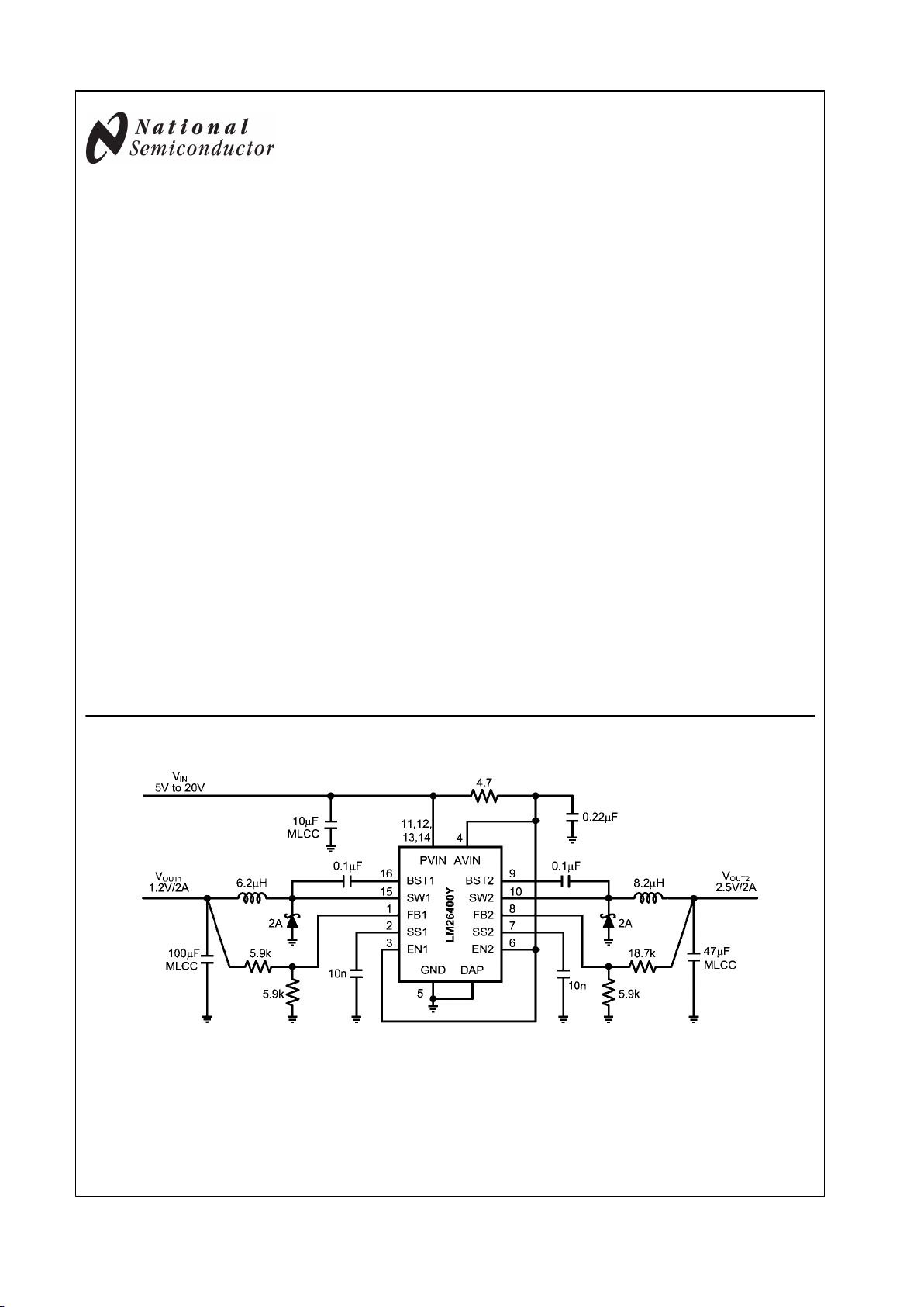
Typical Application
20200252
© 2007 National Semiconductor Corporation 202002 www.national.com
LM26400Y Dual 2A, 500kHz Wide Input Range Buck Regulator
Page 2
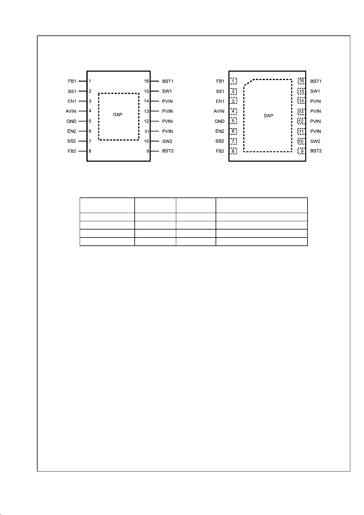
Connection Diagrams
16-Lead ETSSOP (top view)
20200202
NS Package Drawing MXA16A
16-Lead LLP (top view)
20200203
NS Package Drawing SDA16A
Ordering Information
Order Number Package Type
NSC Package
Drawing
Supplied As
LM26400YMH ETSSOP-16 MXA16A Rail of 92 Units
LM26400YMHX ETSSOP-16 MXA16A 2500 Units on Tape and Reel
LM26400YSD LLP-16 SDA16A 1000 Units on Tape and Reel
LM26400YSDX LLP-16 SDA16A 4500 Units on Tape and Reel
www.national.com 2
LM26400Y
Page 3
Pin Descriptions
Pin Name Description
1 FB1
Feedback pin of Channel 1. Connect FB1 to an external voltage divider to set the
output voltage of Channel 1.
2 SS1
Soft start pin of Channel 1. Connect a capacitor between this pin and ground to
program the start up speed.
3 EN1
Enable control input for Channel 1. Logic high enables operation. Do not allow this
pin to float or be greater than VIN + 0.3V.
4 AVIN
Input supply for generating the internal bias used by the entire IC and for generating
the internal bootstrap bias. Needs to be locally bypassed.
5 GND
Signal and Power ground pin. Kelvin connect the lower resistor of the feedback
voltage divider to this pin for good load regulation.
6 EN2
Enable control input for Channel 2. Logic high enables operation. Do not allow this
pin to float or be greater than VIN + 0.3V.
7 SS2
Soft start pin of Channel 2. Connect a capacitor between this pin and ground to
program the start up speed.
8 FB2
Feedback pin of Channel 2. Connect FB2 to an external voltage divider to set the
output voltage of Channel 2.
9 BST2
Supply rail for the gate drive of Channel 2's NMOS switch. A bootstrap capacitor
should be placed between the BST2 and SW2 pins.
10 SW2
Switch node of Channel 2. Connects to the inductor, catch diode, and bootstrap
capacitor.
11, 12, 13,14 PVIN
Input voltage of the power supply. Directly connected to the drain of the internal
NMOS switch. Tie these pins together and connect to a local bypass capacitor.
15 SW1
Switch node of Channel 1. Connects to the inductor, catch diode, and bootstrap
capacitor.
16 BST1
Supply rail for the gate drive of Channel 1's NMOS switch. A bootstrap capacitor
should be placed between the BST1 and SW1 pins.
DAP Die Attach Pad
Must be connected to system ground for low thermal impedance and low grounding
inductance.
3 www.national.com
LM26400Y
Page 4
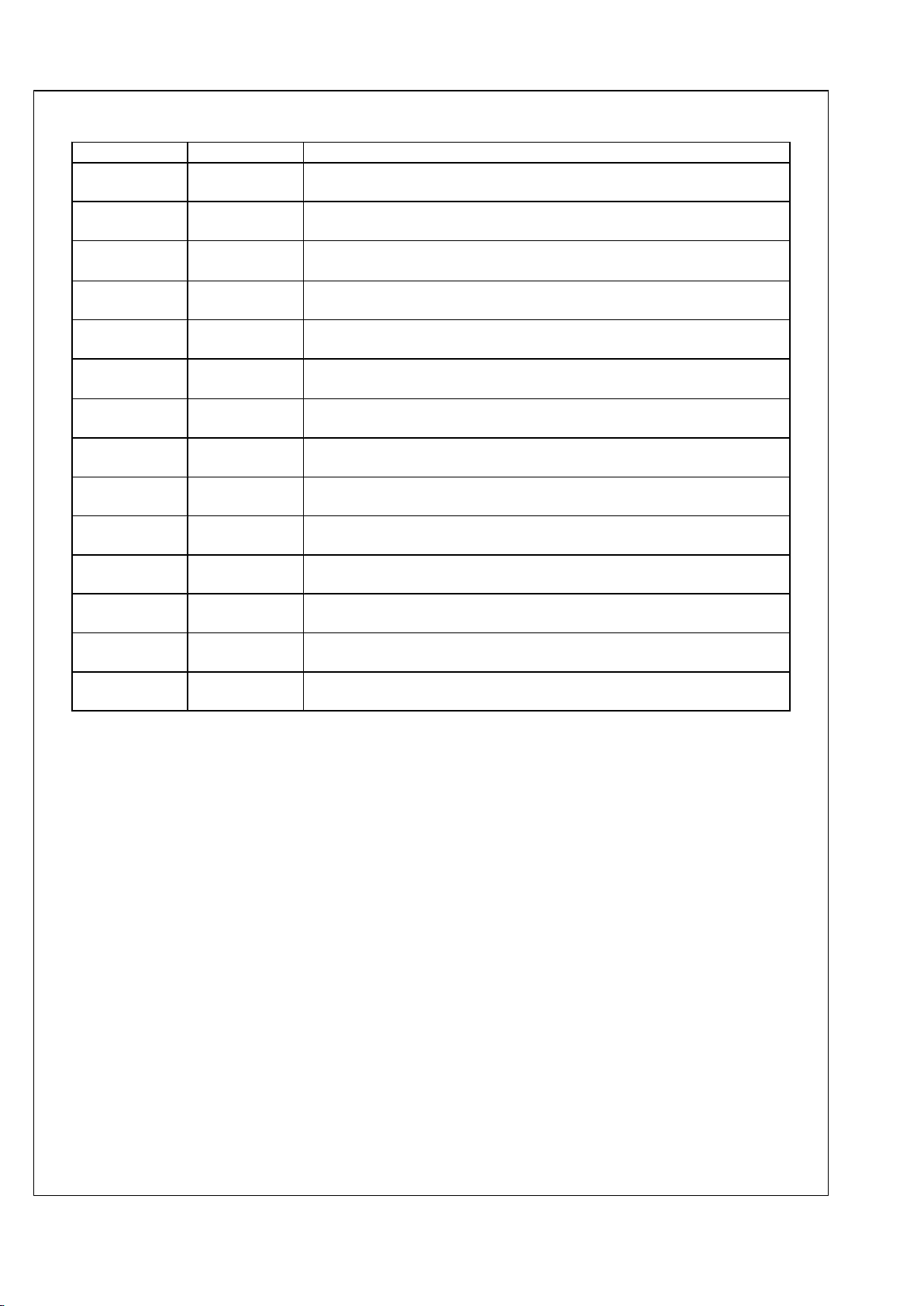
Absolute Maximum Ratings (Note 1)
If Military/Aerospace specified devices are required,
please contact the National Semiconductor Sales Office/
Distributors for availability and specifications.
AVIN, PVIN −0.5V to 22V
SWx Voltage −0.5V to 22V
BSTx Voltage −0.5V to 26V
BSTx to SW Voltage −0.5V to 6V
FBx Voltage −0.5V to 3V
ENx Voltage (Note 2) −0.5V to 22V
SSx Voltage −0.5V to 3V
Junction Temperature +150°C
ESD Susceptibility
Human Body Model (Note 3) 2kV
Storage Temperature Range -65°C to 150°C
Operating Ratings (Note 1)
V
IN
3V to 20V
Junction Temperature −40°C to +125°C
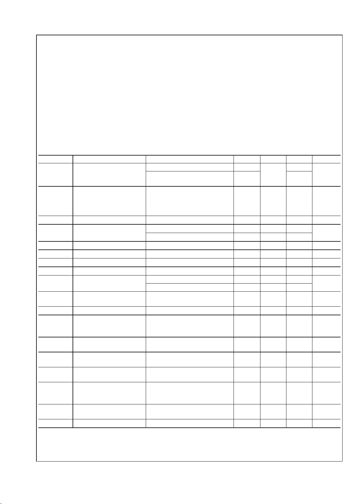
Electrical Characteristics
Unless otherwise stated, the following conditions apply: AVIN = PVIN = VIN = 5V. Limits in standard type are for TJ = 25°C only;
limits in boldface type apply over the junction temperature (TJ) range of -40°C to 125°C. Minimum and Maximum limits are
guaranteed through test, design, or statistical correlation. Typical values represent the most likely parametric norm at TJ = 25°C,
and are provided for reference purposes only.
Symbol Parameter Conditions Min Typ Max Units
V
FB
Voltages at FB1 and FB2 Pins
0°C to 85°C. Feedback Loop Closed. 0.591
0.6
0.611
V
-40°C to 125°C. Feedback Loop
Closed.
0.585 0.617
ΔV
FB_LINE
Line Regulation of FB1 and FB2
Voltages, Expressed as PPM
Change Per Volt of V
IN
Variation
VIN = 3V to 20V
66 ppm/V
I
FB
Current in FB1 and FB2 Pins
VFB = 0.6V
0.4 250 nA
V
UVLO
Under Voltage Lockout
Threshold
VIN Rises From 0V
2.7 2.9
V
VIN Falls From 3.3V
2.0 2.3
V
UVLO_HYS
Hysteresis of UVLO Threshold 0.2 0.36 0.55 V
f
SW
Switching Frequency 0.39 0.52 0.65 MHz
D
MAX
Maximum Duty Cycle 90 96 %
D
MIN
Minimum Duty Cycle 2 %
R
DS_ON
ON Resistance of Internal
Power MOSFET
ETSSOP, 2A Drain Current 175 320
mΩ
LLP, 2A Drain Current 194 350
I
CL
Peak Current Limit of Internal
MOSFET
2.5 3 4.5 A
I
SD
Shutdown Current of AVIN Pin EN1 = EN2 = 0V 2 nA
I
Q
Quiescent Current of AVIN Pin
(both channels are enabled but
not switching)
EN1 = EN2 = 5V, FB1 = FB2 = 0.7V 4 mA
V
EN_IH
Input Logic High of EN1 and
EN2 Pins
2.5 V
V
EN_IL
Input Logic Low of EN1 and
EN2 Pins
0.4 V
I
EN
EN1 and EN2 Currents (sink or
source)
5 nA
I
SW_LEAK
Switch Leakage Current
Measured at SW1 and SW2
Pins
EN1 = EN2 = SWx = 0 1 µA
ΔΦ
Phase Shift Between SW1 and
SW2 Rising Edges
Feedback Loop Closed. Continuous
Conduction Mode.
170 180 190 deg
I
SS
SSx Pin Current 11 16 21 µA
www.national.com 4
LM26400Y
Page 5
Symbol Parameter Conditions Min Typ Max Units
ΔI
SS
Difference Between SS1 and
SS2 Currents
3 µA
V
FB_F
FB1 and FB2 Frequency Foldback Threshold
0.35 V
Thermal Characteristics
Symbol Description Conditions
Typical Value
Unit
TSSOP LLP
θ
JA
Junction-to-Ambient Thermal
Resistance (Note 4)
Mount package on a standard board (Note 5) and
test per JESD51-7 standard.
28 26
°C/W
θ
JC
Junction-to-Case-Bottom
Thermal Resistance
3 2.8
T
SD
Thermal Shutdown
Threshold
Junction temperature rises. 165
°C
T
SD_HYS
Thermal Shutdown
Hysteresis
Junction temperature falls from above TSD.
15
Note 1: Absolute maximum ratings indicate limits beyond which damage to the device may occur. Operating Ratings are conditions under which the device is
intended to be functional, but specific performance is not guaranteed. For guaranteed performance limits and associated test conditions, see Electrical
Characteristics table.
Note 2: EN1 and EN2 pins should never be higher than VIN + 0.3V.
Note 3: The human body model is a 100pF capacitor discharged through a 1.5 kΩ resistor into each pin. Test method is per JESD-22-A114.
Note 4: Value is highly board-dependent. For comparison of package thermal performance only. Not recommended for prediction of junction temperature in real
applications. See THERMAL CONSIDERATIONS for more information.
Note 5: A standard board refers to a four-layer PCB with the size 4.5”x3”x0.063”. Top and bottom copper is 2 oz. Internal plane copper is 1 oz. For details refer
to JESD51-7 standard.
5 www.national.com
LM26400Y
Page 6
Typical Performance Characteristics Unless otherwise specified or thermal-shutdown related, T
A
= 25°
C for efficiency curves, loop gain plots and waveforms, and TJ = 25°C for all others.
Efficiency, V
OUT
= 5V
20200237
Efficiency, V
OUT
= 3.3V
20200216
Efficiency, V
OUT
= 2.5V
20200217
Efficiency, V
OUT
= 1.2V
20200218
AVIN Shutdown Current vs. Temperature
20200206
VIN Shutdown Current vs. V
IN
20200238
www.national.com 6
LM26400Y
Page 7
Switching Frequency vs. Temperature
20200207
Feedback Voltage vs. Temperature
20200208
Feedback Voltage vs. V
IN
20200209
Frequency Foldback
20200210
SS-Pin Current vs. Temperature
20200278
FET R
DS_ON
vs. Temperature
20200221
7 www.national.com
LM26400Y
Page 8
Switch Current Limit vs. Temperature
20200234
Loop Gain, CCM
20200219
Loop Gain, DCM
20200220
Loop Gain, CCM
20200236
Loop Gain, DCM
20200222
Load Step Response
20200223
www.national.com 8
LM26400Y
Page 9

Load Step Response
20200224
Line Transient Response
20200227
Start-Up (No Load)
20200228
Start-Up (No Load)
20200239
Shutdown
20200229
Thermal Shutdown
20200230
9 www.national.com
LM26400Y
Page 10

Recovery from Thermal Shutdown
20200240
Short-circuit Triggering
20200231
Short-circuit Release
20200232
www.national.com 10
LM26400Y
Page 11

Block Diagram
20200204
11 www.national.com
LM26400Y
Page 12

Application Hints
GENERAL
The LM26400Y is a dual PWM peak-current mode buck regulator with two integrated power MOSFET switches. The part
is designed to be easy to use. The two regulators are mostly
identical and share the same input voltage and the same reference voltage (0.6V). The two PWM clocks are of the same
frequency but 180° out of phase. The two channels can have
different soft-start ramp slopes and can be turned on and off
independently.
Loop compensation is built in. The feedback loop design is
optimized for ceramic output capacitors.
Since the power switches are built in, the achievable output
current level also has to do with thermal environment of the
specific application. The LM26400Y enters thermal shutdown
when the junction temperature exceeds 165°C or so.
START-UP AND SHUTDOWN
During a soft-start, the ramp of the output voltage is proportional to the ramp of the SS pin. When the EN pin is pulled
high, an internal 16µA current source starts to charge the corresponding SS pin. The capacitance between the SS pin and
ground determines how fast the SS voltage ramps up. The
non-inverting input of the transconductance error amplifier,
i.e. the moving reference during soft-start, will be the lower of
SS voltage and the 0.6V reference (V
REF
). So before SS
reaches 0.6V, the reference to the error amplifier will be the
SS voltage. When SS exceeds 0.6V, the non-inverting input
of the transconductance amplifier will be a constant 0.6V and
that will be the time soft-start ends. The SS voltage will continue to ramp all the way up to the internal 2.7V supply voltage
before leveling off.
To calculate the needed SS capacitance for a given soft-start
duration, use the following equation.
ISS is SS pin charging current, typically 16µA. V
REF
is the internal reference voltage, typically 0.6V. tSS is the desired softstart duration. For example, if 1ms is the desired soft-start
time, then the nominal SS capacitance should be 25nF. Apply
tolerances if necessary. Use the VFB entry in the Electrical
Characteristic table for the V
REF
tolerance.
Inductor current during soft-start can be calculated by the following equation.
V
OUT
is the target output voltage, I
OUT
is the load current dur-
ing start-up, and C
OUT
is the output capacitance. For example,
if the output capacitor is 10µF, output voltage is 2.5V, softstart capacitor is 10nF and there is no load, then the average
inductor current during soft-start will be 62.5mA.
When EN pin is pulled below 0.4V or so, the 16µA current
source will stop charging the SS pin. The SS pin will be discharged through a 330Ω internal FET to ground. During this
time, the internal power switch will remain turned off while the
output is discharged by the load.
If EN is again pulled high before SS and output voltage are
completely discharged, soft-start will begin with a non-zero
reference and the level of the soft-start reference will be the
lower of SS voltage and 0.6V.
When the output is pre-biased, the LM26400Y can usually
start up successfully if there is at least a 2-Volt difference between the input voltage and the pre-bias. An output pre-bias
condition refers to the case when the output is sitting at a nonzero voltage at the beginning of a start-up. The key to a
successful start-up under such a situation is enough initial
voltage across the bootstrap capacitor. When an output prebias condition is anticipated, the power supply designer
should check the start-up behavior under the highest potential
pre-bias.
A pre-bias condition caused by a glitch in the enable signal
after start-up or by an input brown-out condition normally is
not an issue because the bootstrap capacitor holds its charge
much longer than the output capacitor(s).
Due to the frequency foldback mechanism, the switching frequency during start-up will be lower than the normal value
before VFB reaches 0.35V or so. See Frequency Foldback plot
in the Typical Performance Characteristics section.
It is generally okay to connect the EN pin to VIN to simplify the
system design. However, if the VIN ramp is slow and the load
current is relatively high during soft-start, the V
OUT
ramp may
have a notch in it and a slight overshoot at the end of startup.
This is due to the reduced load current handling capability of
the LM26400Y for VIN lower than 5V. If this kind of behavior
is a problem for the system designer, there are two solutions.
One is to control the EN pin with a logic signal and do not pull
the EN high until VIN is above 5V or so. Make sure the logic
signal is never higher than VIN by 0.3V. The other is to use an
external 5V bootstrap bias if it is ready before VIN hits 2.7V or
so. See LOW INPUT VOLTAGE CONSIDERATIONS section
for more information.
OVER-CURRENT PROTECTION
The instantaneous switch current is limited to a typical of 3
Amperes. Any time the switch current reaches that value, the
switch will be turned off immediately. This will result in a
smaller duty cycle than normal, which will cause the output
voltage to dip. The output voltage will continue drooping until
the load draws a current that is equal to the peak-limited inductor current. As the output voltage droops, the FB pin
voltage will also droop proportionally. When the FB voltage
dips below 0.35V or so, the PWM frequency will start to decrease. The lower the FB voltage the lower the PWM frequency. See Frequency Foldback plot in the Typical Performance Characteristics section.
The frequency foldback helps two things. One is to prevent
the switch current from running away as a result of the finite
minimum ON time (40 ns or so for the LM26400Y) and the
small duty cycle caused by lowered output voltage due to the
current limit. The other is it also helps reduce thermal stress
both in the IC and the external diode.
The current limit threshold of the LM26400Y remains constant
over all duty cycles.
One thing to pay attention to is that recovery from an overcurrent condition does not go through a soft-start process.
This is because the reference voltage at the non-inverting input of the error amplifier always sits at 0.6V during the overcurrent protection. So if the over-current condition is suddenly
removed, the regulator will bring the FB voltage back to 0.6V
as quickly as possible. This may cause an overshoot in the
output voltage. Generally, the larger the inductor or the lower
the output capacitance the more the overshoot, and vice versa. If the amount of such overshoot exceeds the allowed limit
for a system, add a CFF capacitor in parallel with the upper
www.national.com 12
LM26400Y
Page 13

feedback resistor to eliminate the overshoot. See the section
LOAD STEP RESPONSE for more details on CFF.
When one channel gets into over-current protection mode,
the operation of the other channel will not be affected.
LOOP STABILITY
To the first order approximation, the LM26400Y has a VFB-toInductor Current transfer admittance (i.e. ratio of inductor
current to FB pin voltage, in frequency domain) close to the
plot in Figure 1. The transfer admittance has a DC value of
104dBS (dBS stands for decibel Siemens. The equivelant of
0dBS is 1 Siemens.). There is a pole at 1Hz and a zero at
approximately 8kHz. The plateau after the 8kHz zero is about
27dBS. There are also high frequency poles that are not
shown in the figure. They include a double pole at 1.2MHz or
so, and another double pole at half the switching frequency.
Depending on factors such as inductor ripple size and duty
cycle, the double pole at half the switching frequency may
become two separate poles near half the switching frequency.
20200250
FIGURE 1. VFB-to-Inductor Current Transfer Admittance
An easy strategy to build a stable loop with reasonable phase
margin is to try to cross over between 20kHz and 100kHz,
assuming the output capacitor is ceramic. When using pure
ceramic capacitors at the output, simply use the following
equation to find out the crossover frequency.
where 22S (22 Siemens) is the equivelant of the 27dBS transfer admittance mentioned above and r is the ratio of 0.6V to
the output voltage. Use the same equation to find out the
needed output capacitance for a given crossover frequency.
Phase margin is typically between 50° and 60°. Notice the
above equation is only good for a crossover between 20kHz
and 100kHz. A crossover frequency outside this range may
result in lower phase margin and less accurate prediction by
the above equation.
Example: V
OUT
= 2.5V, C
OUT
= 36µF, find out the crossover
frequency.
Assume the crossover is between 20kHz and 100kHz. Then
The above analysis serves as a starting point. It is a good
practice to always verify loop gain on bench.
LOAD STEP RESPONSE
In general, the excursion in output voltage caused by a load
step can be reduced by increasing the output capacitance.
Besides that, increasing the small-signal loop bandwidth also
helps. This can be achieved by adding a 27nF or so capacitor
(CFF) in parallel with the upper feedback resistor (assuming
the lower feedback resistor is 5.9kΩ). See Figure 2 for an illustration.
20200251
FIGURE 2. Adding a CFF Capacitor
The responses to a load step between 0.2A and 2A with and
without a CFF are shown in Figure 3. The higher loop bandwidth as a result of CFF reduces the total output excursion by
about 80mV.
20200242
FIGURE 3. CFF Improves Load Step Response
Use the following equation to calculate the new loop bandwidth:
Again, the assumption is the crossover is between 20kHz and
100kHz.
In an extreme case where the load goes to less than 100mA
during a large load step, output voltage may exhibit extra un-
13 www.national.com
LM26400Y
Page 14

dershoot. This usually happens when the load toggles high at
the time V
OUT
just ramps down to its regulation level from an
overshoot. Figure 4 shows such a case where the load toggles between 1.7A and only 50mA.
20200241
FIGURE 4. Extreme Load Step
In the example, the load first goes down to 50mA quickly
(0.9A/µs), causing a 90µs no-switching period, and then
quickly goes up to 1.7A when V
OUT1
just hits its regulation
level (1.2V), resulting in a large dip of 440mV in the output
voltage.
If it is known in a system design that the load can go down to
less than 100mA during a load step, and that the load can
toggle high any time after it toggles low, take the following
measures to minimize the potential extra undershoot. First is
to add the Cff mentioned above. Second is to increase the
output capacitance.
For example, to meet a ±10% V
OUT
excursion requirement for
a 100mA to 2A load step, approximately 200µF output capacitance is needed for a 1.2V output, and about 44µF is
needed for a 5V output.
LOW INPUT VOLTAGE CONSIDERATIONS
When VIN is between 3V and 5V, it is recommended that an
external bootstrap bias voltage and a Schottky diode be used
to handle load currents up to 2A. See Figure 5 for an illustration.
20200244
FIGURE 5. External Bootstrap for Low V
IN
The recommended voltage for the external bias is 5V. Due to
the absolute maximum rating of V
BST
- VSW, the external 5V
bias should not be higher than 6V.
THERMAL SHUTDOWN
Whenever the junction temperature of the LM26400Y exceeds 165°C, the MOSFET switch will be kept off until the
temperature drops below 150°C, at which point the regulator
will go through a hard-start to quickly raise the output voltage
back to normal. Since it is a hard-start, there will be an overshoot at the output. See Thermal Shutdown in the Typical
Performance Characteristics section.
POWER LOSS ESTIMATION
The total power loss in the LM26400Y comprises of three
parts - the power FET conduction loss, the power FET switching loss and the IC's housekeeping power loss. Use the
following equation to estimate the conduction loss.
where TJ is the junction temperature or the target junction
temperature if the former is unknown. RDS is the ON resistance of the internal FET at room temperature. Use 180mΩ
for RDS if the actual value is unknown.
Use the following equation to estimate the switching loss.
Another loss in the IC is the housekeeping loss. It is the power
dissipated by circuitry in the IC other than the power FETs.
The equation is:
The 15mW is gate drive loss. Do the calculation for both
channels and find out the total power loss in the IC.
The power loss calculation can help estimate the overall power supply efficiency.
Example:
VIN = 12V, V
OUT1
= 1.2V, I
OUT1
= 2A, V
OUT2
= 2.5V, I
OUT2
= 2A.
Target junction temperature is 90°C.
So conduction loss in Channel 1 is:
Conduction loss in Channel 2 is:
Switching loss in either channel is:
www.national.com 14
LM26400Y
Page 15

House keeping loss is:
Finally the total power loss in the LM26400Y is:
PROGRAMMING OUTPUT VOLTAGE
First make sure the required maximum duty cycle in steady
state is less than 80% so that the regulator will not lose regulation. The datasheet lower limit for maximum duty cycle is
about 90% over temperature (see Electrical Characteristics
table for the accurate value). The maximum duty cycle in
steady state happens at low line and full load.
The output voltage is programmed through the feedback resistors R1 and R2, as illustrated in Figure 6.
20200258
FIGURE 6. Programming Output Voltage
It is recommended that the lower feedback resistor R2 always
be 5.9kΩ. This simplifies the selection of the CFF value (For
an explanation of CFF, please refer to the section LOAD STEP
RESPONSE). The 5.9kΩ is also a suitable R2 value in applications that need to increase the output voltage on the fly by
paralleling another resistor with R2. Since the FB pin is 0.6V
during normal operation, the current through the feedback resistors is normally 0.6V / 5.9kΩ = 0.1mA and the power
dissipation in R2 is 0.6V x 0.6V / 5.9kΩ = 61µW - low enough
for 0402 size or smaller resistors.
Use the following equation to determine the upper feedback
resistor R1.
To determine the maximum allowed resistor tolerance, use
the following equation:
where TOL is the set point accuracy of the regulator, Φ is the
tolerance of VFB.
Example:
V
OUT
= 1.2V, with a set point accuracy of +/-3.5%.
Choose 1% resistors. R2 = 5.90kΩ.
INDUCTOR SELECTION
An inductance value that gives a peak-to-peak ripple current
of 0.4A to 0.8A is recommended. Too large a ripple current
can reduce the maximum achievable DC load current because the peak current of the switch is limited to a typical of
3A. Too small a ripple current can cause the regulator to oscillate due to the lack of inductor current ramp signal, especially under high input voltages. Use the following equation to
determine inductance:
where V
IN_MAX
is the maximum input voltage of the applica-
tion.
The rated current of the inductor should be higher than the
maximum DC load current. Generally speaking, the lower the
DC resistance of the inductor winding, the higher the overall
regulator efficiency.
Ferrite core inductors are recommended for less AC loss and
less fringing magnetic flux. The drawback of ferrite core inductors is their quick saturation characteristic. Once the inductor gets saturated, its current can spike up very quickly if
the switch is not turned off immediately. The current limit circuit has a propagation delay and so is oftentimes not fast
enough to stop the saturated inductor from going above the
current limit. This has the potential to damage the internal
switch. So to prevent a ferrite core inductor from getting into
saturation, the inductor saturation current rating should be
higher than the switch current limit ICL. The LM26400Y is quite
robust in handling short pulses of current that is a few amps
above the current limit. When a compromise has to be made,
pick an inductor with a saturation current just above the lower
limit of the ICL. Be sure to validate the short-circuit protection
over the intended temperature range.
To prevent the inductor from saturating over the entire -40°C
to 125°C range, pick one with a saturation current higher than
the upper limit of ICL in the Electrical Characteristics table.
Inductor saturation current is usually lower when hot. So consult the inductor vendor if the saturation current rating is only
specified at room temperature.
Soft saturation inductors such as the iron powder types can
also be used. Such inductors do not saturate suddenly and
therefore are safer when there is a severe overload or even
shorted output. Their physical sizes are usually smaller than
the Ferrite core inductors. The downside is their fringing flux
and higher power dissipation due to relatively high AC loss,
especially at high frequencies.
Example:
V
OUT
= 1.2V; VIN = 9V to 14V; I
OUT
= 2A max; Peak-to-peak
Ripple Current ΔI = 0.6A.
15 www.national.com
LM26400Y
Page 16

Choose a 5µH or so ferrite core inductor that has a saturation
current around 3A at room temperature. For example,
Sumida's CDRH6D26NP-5R0NC.
If the maximum load current is significantly lower than 2A, pick
an inductor with the same saturation rating as a 2A design but
with a lowered DC current rating. That should result in a
smaller inductor. There are not many choices, though. Another possibility is to use a soft saturation type inductor,
whose size will be dominated by the DC current rating.
OUTPUT CAPACITOR SELECTION
Output capacitors in a buck regulator handles the AC current
from the inductor and so have little ripple RMS current and
their power dissipation is not a concern. The concern usually
revolves around loop stability and capacitance retention.
The LM26400Y's internal loop compensation was designed
around ceramic output capacitors. From a stability point of
view, the lower the output voltage, the more capacitance is
needed.
Below is a quick summary of temperature characteristics of
some commonly used ceramic capacitors. So an X7R ceramic capacitor means its capacitance can vary ±15% over the
temperature range of -55°C to +125°C.
Capacitance Variation Over Temperature (Class II
Dielectric Ceramic Capacitors)
Low
Temperature
High
Temperature
Capacitance Change
Range
X: -55°C 5: +85°C R: ±15%
Y: -30°C 6: +105°C S: ±22%
Z: +10°C 7: +125°C U: +22%, -56%
8: +150°C V: +22%, -82%
Besides the variation of capacitance over temperature, the
actual capacitance of ceramic capacitors also vary, sometimes significantly, with applied DC voltage. Figure 7 illustrates such a characteristic of several ceramic capacitors of
various physical sizes from Murata. Unless the DC voltage
across the capacitor is going to be small relative to its rated
value, going to too small a physical size will have the penalty
of losing significant capacitance during circuit operation.
20200245
FIGURE 7. Capacitance vs. Applied DC Voltage
The amount of output capacitance directly contributes to the
output voltage ripple magnitude. A quick way to estimate the
output voltage ripple is to multiply the inductor peak-to-peak
ripple current by the impedance of the output capacitors. For
example, if the inductor ripple current is 0.6A peak-to-peak,
and the output capacitance is 44µF, then the output voltage
ripple should be close to 0.6A x (6.28 x 500kHz x 44µF)-1 =
4.3mV. Sometimes when a large ceramic capacitor is used,
the switching frequency may be higher than the capacitor's
self resonance frequency. In that case, find out the true
impedance at the switching frequency and then multiply that
value by the ripple current to get the ripple voltage.
The amount of output capacitance also impacts the stability
of the feedback loop. Refer to the LOOP STABILITY section
for guidelines.
INPUT CAPACITOR SELECTION
The input capacitors provide the AC current needed by the
nearby power switch so that current provided by the upstream
power supply does not carry a lot of AC content, generating
less EMI. To the buck regulator in question, the input capacitor also prevents the drain voltage of the FET switch from
dipping when the FET is turned on, therefore providing a
healthy line rail for the LM26400Y to work with. Since typically
most of the AC current is provided by the local input capacitors, the power loss in those capacitors can be a concern. In
the case of the LM26400Y regulator, since the two channels
operate 180° out of phase, the AC stress in the input capacitors is less than if they operated in phase. The measure for
the AC stress is called input ripple RMS current. It is strongly
recommended that at least one 4.7µF ceramic capacitor be
placed next to the PVIN pins. Bulk capacitors such as electrolytic capacitors or OSCON capacitors can be added to help
stabilize the local line voltage, especially during large load
transient events. As for the ceramic capacitors, use X7R , X6S
or X5R types. They maintain most of their capacitance over
a wide temperature range. Try to avoid sizes smaller than
0805. Otherwise significant drop in capacitance may be
caused by the DC bias voltage. See OUTPUT CAPACITOR
SELECTION section for more information. The DC voltage
rating of the ceramic capacitor should be higher than the
highest input voltage.
Capacitor temperature is a major concern in board designs.
While using a 4.7µF or higher MLCC as the input capacitor is
a good starting point, it is a good idea to check the temperature in the real thermal environment to make sure the capacitors are not over heated. Capacitor vendors may provide
curves of ripple RMS current vs. temperature rise, based on
a designated thermal impedance. In reality, the thermal
impedance may be very different. So it is always a good idea
to check the capacitor temperature on the board.
Since the duty cycles of the two channels may overlap, calculation of the input ripple RMS current is a little tedious. Use
the following equation.
I1 is Channel 1's maximum output current. I2 is Channel 2's
maximum output current. d1 is the non-overlapping portion of
Channel 1's duty cycle D1. d2 is the non-overlapping portion
of Channel 2's duty cycle D2. d3 is the overlapping portion of
the two duty cycles. Iav is the average input current. Iav=
I1·D1 + I2·D2. To quickly determine the values of d1, d2 and
d3, refer to the decision tree in Figure 8. To determine the
duty cycle of each channel, use D = V
OUT/VIN
for a quick result
or use the following equation for a more accurate result.
www.national.com 16
LM26400Y
Page 17

RDC is the winding resistance of the inductor. RDS is the ON
resistance of the MOSFET switch.
Example:
VIN = 5V, V
OUT1
= 3.3V, I
OUT1
= 2A, V
OUT2
= 1.2V, I
OUT2
= 1.5A,
RDS = 170mΩ, RDC = 30mΩ. (I
OUT1
is the same as I1 in the
input ripple RMS current equation, I
OUT2
is the same as I2).
First, find out the duty cycles. Plug the numbers into the duty
cycle equation and we get D1 = 0.75, and D2 = 0.33. Next,
follow the decision tree in Figure 8 to find out the values of d1,
d2 and d3. In this case, d1 = 0.5, d2 = D2 + 0.5 - D1 = 0.08,
and d3 = D1 - 0.5 = 0.25. Iav = I
OUT1
·D1 + I
OUT2
·D2 = 1.995A.
Plug all the numbers into the input ripple RMS current equation and the result is I
irrm
= 0.77A.
20200246
FIGURE 8. Determining d1, d2 and d3
CATCH DIODE SELECTION
The catch diode should be at least 2A rated. The most stressful operation for the diode is usually when the output is shorted
under high line. Always pick a Schottky diode for its lower
forward drop and higher efficiency. The reverse voltage rating
of the diode should be at least 25% higher than the highest
input voltage. The diode junction temperature is a main concern here. Always validate the diode's junction temperature
in the intended thermal environment to make sure its thermally derated maximum current is not exceeded. There are a
few 2A, 30V surface mount Schottky diodes available in the
market. Notice that diodes have a negative temperature coefficient, so do not put two diodes in parallel to achieve a lower
temperature rise. Current will be hogged by one of the diodes
instead of shared by the two. Use a larger package for that
purpose.
THERMAL CONSIDERATIONS
Due to the low thermal impedance from junction to the dieattach pad (or DAP, exposed metal at the bottom of the
package), thermal performance heavily depends on PCB
copper arrangement. The minimum requirement is to have a
top-layer thermal pad that is exactly the same size as the
DAP. There should be at least nine 8-mil thermal vias in the
pad. The thermal vias should be connected to internal ground
plane(s) (if available) and to a ground plane on the bottom
layer that is as large as allowed.
In boards that have internal ground planes, extending the toplayer thermal pad outside the body of the package to form a
"dogbone" shape offers little performance improvement.
However, for two-layer boards, the dogbone shape on the top
layer will provide significant help.
Predicting on paper with reasonable accuracy the junction
temperature of the LM26400Y in a real-world application is
still an art. Major factors that contribute to the junction temperature but not directly associated with the thermal performance of the LM26400Y itself include air speed, air
temperature, nearby heating elements and arrangement of
PCB copper connected to the DAP of the LM26400Y. The
θJA value published in the datasheet is based on a standard
board design in a single heating element mode and measured
in a standard environment. The real application is usually
completely different from those conditions. So the actual θ
JA
will be significantly different from the datasheet number. The
best approach is still to assign as much copper area as allowed to the DAP and prototype the design.
When prototyping the design, it is necessary to know the
junction temperature of the LM26400Y to assess the thermal
margin. The best way to measure the LM26400Y's junction
temperature when the board is working in its usual mode is to
measure the package-top temperature using an infrared thermal imaging camera. Look for the highest temperature reading across the case-top. Add two degrees to the measurement result and the number should be a pretty good estimate
of the junction temperature. Due to the high temperature gra-
17 www.national.com
LM26400Y
Page 18

dient across the case-top, the use of a thermal couple is
generally not recommended. If a thermal couple has to be
used, try to locate the hottest spot on the case-top first and
then secure the thermal couple at exactly the same location.
The thermal couple needs to be a light-gauge type (such as
40-gauge). Apply a small blob of thermal compound to the
contact point and then secure the thermal couple on the casetop using thermally non-conductive glue.
If the maximum allowed junction temperature is exceeded,
load current has to be lowered to bring the temperature back
in specification. Or better thermal management such as more
air flow needs to be provided.
As a summary, here is a list of important items to consider:
1. Use multi-layer PC boards with internal ground planes.
2. Use nine or more thermal vias to connect the top-layer
thermal pad to internal ground plane(s) and ground copper on
the bottom layer.
3. Generate as large a ground plane as allowable on outer
layers, especially near the package.
4. Use 2 oz. copper whenever possible.
5. Try to spread out heat generating components.
6. The inductors and diodes are heat generating components
and should be connected to power or ground planes using
many vias.
LAYOUT GUIDELINES
There are mainly two considerations for PCB layout - thermal
and electrical. For thermal details, refer to the section THERMAL CONSIDERATIONS. Electrical wise, follow the rules
below as much as possible. In general, the LM26400Y is a
quite robust part in terms of insensitivity to different layout
patterns or even abuses.
1. Keep the input ceramic capacitor(s) as close to the PVIN
pins as possible.
2. Use internal ground planes when available.
3. The SW pins are high current carrying pins so traces connected to them should be short and fat.
4. Keep feedback resistors close to the FB pins.
5. Keep the AVIN RC filter close to the AVIN pin.
6. Keep the voltage feedback traces away from the switch
nodes.
7. Use six or more vias next to the ground pad of the catch
diode.
8. Use at least four vias next to the ground pad of output capacitors.
9. Use at least four vias next to each pad of the input capacitors.
For low EMI emission, try not to assign large areas of copper
to the noisy switch nodes as a heat sinking method. Instead,
assign a lot of copper to the output nodes.
20200243
FIGURE 9. PCB Layout Example
www.national.com 18
LM26400Y
Page 19

LM26400Y Design Examples
20200253
FIGURE 10. Example Circuit 1
Bill of Materials (Circuit 1, VIN = 12V±10%, Output1 = 1.2V/2A, Output2 = 2.5V/2A)
Part Description Part Values Physical Size Part Number Manufacturer
C1 Capacitor, Ceramic 10µF, 16V, X5R 1210 GRM32DR61C106KA01 Murata
C2 Capacitor, Ceramic 0.22µF, 16V, X5R 0603 EMK107BJ224KA-T Taiyo Yuden
C3 Capacitor, Ceramic 0.1µF, 6.3V, X5R 0402 C1005X5R0J104K TDK
C4 Capacitor, Ceramic 0.1µF, 6.3V, X5R 0402 C1005X5R0J104K TDK
C5 Capacitor, Ceramic 100µF, 6.3V, X5R 1210 GRM32ER60J107ME20L Murata
C6 Capacitor, Ceramic 47µF, 6.3V, X5R 1210 GRM32ER60J476ME20L Murata
C7 Capacitor, Ceramic 0.012µF, 6.3V, X5R 0402 C0402C123K9PACTU Kemet
C8 Capacitor, Ceramic 0.012µF, 6.3V, X5R 0402 C0402C123K9PACTU Kemet
C9 Capacitor, Ceramic 0.027µF, 6.3V, X5R 0402 C0402C273K9PACTU Kemet
C10 Capacitor, Ceramic 0.027µF, 6.3V, X5R 0402 C0402C273K9PACTU Kemet
D1 Diode, Schottky 2A, 30V SMB MBRS230LT3G ON Semiconductor
D2 Diode, Schottky 2A, 30V SMB MBRS230LT3G ON Semiconductor
L1 Inductor 5µH, 2.2A
7x7x2.8 mm
3
CDRH6D26NP-5R0NC Sumida
L2 Inductor 8.7µH, 2.2A
7x7x4 mm
3
CDRH6D38NP-8R7NC Sumida
R1 Resistor
10.0Ω, 1%
0402 CRCW040210R0FK Vishay
R2 Resistor
5.90kΩ, 1%
0402 CRCW04025K90FK Vishay
R3 Resistor
5.90kΩ, 1%
0402 CRCW04025K90FK Vishay
R4 Resistor
18.7kΩ, 1%
0402 CRCW040218K7FK Vishay
R5 Resistor
5.90kΩ, 1%
0402 CRCW04025K90FK Vishay
U1 Regulator Dual 2A Buck ETSSOP-16 LM26400YMH
National
Semiconductor
19 www.national.com
LM26400Y
Page 20

LM26400Y Design Examples
Bill of Materials (Circuit 1, VIN = 7V to 20V, Output1 = 3.3V/2A, Output2 = 5V/2A)
Part Description Part Values Physical Size Part Number Manufacturer
C1 Capacitor, Ceramic 10µF, 25V, X5R 1812 GRM43DR61E106KA12 Murata
C2 Capacitor, Ceramic 0.22µF, 25V, X5R 0603 TMK107BJ224KA-T Taiyo Yuden
C3 Capacitor, Ceramic 0.1µF, 6.3V, X5R 0402 C1005X5R0J104K TDK
C4 Capacitor, Ceramic 0.1µF, 6.3V, X5R 0402 C1005X5R0J104K TDK
C5 Capacitor, Ceramic 47µF, 6.3V, X5R 1210 GRM32ER60J476ME20 Murata
C6 Capacitor, Ceramic 33µF, 6.3V, X5R 1210 GRM32DR60J336ME19 Murata
C7 Capacitor, Ceramic 0.012µF, 6.3V, X5R 0402 C0402C123K9PACTU Kemet
C8 Capacitor, Ceramic 0.012µF, 6.3V, X5R 0402 C0402C123K9PACTU Kemet
C9 Capacitor, Ceramic 0.027µF, 6.3V, X5R 0402 C0402C273K9PACTU Kemet
C10 Capacitor, Ceramic 0.027µF, 6.3V, X5R 0402 C0402C273K9PACTU Kemet
D1 Diode, Schottky 2A, 30V SMB MBRS230LT3G ON Semiconductor
D2 Diode, Schottky 2A, 30V SMB MBRS230LT3G ON Semiconductor
L1 Inductor 10µH, 3A
8.3x8.3x4 mm
3
CDRH8D38NP-100NC Sumida
L2 Inductor 15µH, 3A
8.3x8.3x4 mm
3
CDRH8D43/HP-150NC Sumida
R1 Resistor
10.0Ω, 1%
0402 CRCW040210R0FK Vishay
R2 Resistor
26.7kΩ, 1%
0402 CRCW040226K7FK Vishay
R3 Resistor
5.90kΩ, 1%
0402 CRCW04025K90FK Vishay
R4 Resistor
43.2kΩ, 1%
0402 CRCW040218K7FK Vishay
R5 Resistor
5.90kΩ, 1%
0402 CRCW04025K90FK Vishay
U1 Regulator Dual 2A Buck ETSSOP-16 LM26400YMH
National
Semiconductor
www.national.com 20
LM26400Y
Page 21

LM26400Y Design Examples
20200255
FIGURE 11. Example Circuit 2
Bill of Materials (Circuit 2, VIN = 3V to 5V, Output1 = 1.2V/2A, Output2 = 1.8V/2A)
Part Description Part Values Physical Size Part Number Manufacturer
C1 Capacitor, Ceramic 10µF, 6.3V, X5R 1206 GRM319R60J106KE19 Murata
C2 Capacitor, Ceramic 0.22µF, 6.3V, X5R 0402 JMK105BJ224KV-F Taiyo Yuden
C3 Capacitor, Ceramic 0.1µF, 6.3V, X5R 0402 C1005X5R0J104K TDK
C4 Capacitor, Ceramic 0.1µF, 6.3V, X5R 0402 C1005X5R0J104K TDK
C5 Capacitor, Ceramic 100µF, 6.3V, X5R 1210 GRM32ER60J107ME20L Murata
C6 Capacitor, Ceramic 100µF, 6.3V, X5R 1210 GRM32ER60J107ME20L Murata
C7 Capacitor, Ceramic 0.012µF, 6.3V, X5R 0402 C0402C123K9PACTU Kemet
C8 Capacitor, Ceramic 0.012µF, 6.3V, X5R 0402 C0402C123K9PACTU Kemet
C9 Capacitor, Ceramic 0.027µF, 6.3V, X5R 0402 C0402C273K9PACTU Kemet
C10 Capacitor, Ceramic 0.027µF, 6.3V, X5R 0402 C0402C273K9PACTU Kemet
D1 Diode, Schottky 2A, 30V SMB MBRS230LT3G ON Semiconductor
D2 Diode, Schottky 2A, 30V SMB MBRS230LT3G ON Semiconductor
L1 Inductor 5µH, 2.2A
7x7x2.8 mm
3
CDRH6D26NP-5R0NC Sumida
L2 Inductor 5µH, 2.2A
7x7x2.8 mm
3
CDRH6D26NP-5R0NC Sumida
R1 Resistor
10.0Ω, 1%
0402 CRCW040210R0FK Vishay
R2 Resistor
5.90kΩ, 1%
0402 CRCW04025K90FK Vishay
R3 Resistor
5.90kΩ, 1%
0402 CRCW04025K90FK Vishay
R4 Resistor
11.8kΩ, 1%
0402 CRCW040211K8FK Vishay
R5 Resistor
5.90kΩ, 1%
0402 CRCW04025K90FK Vishay
U1 Regulator Dual 2A Buck ETSSOP-16 LM26400YMH
National
Semiconductor
21 www.national.com
LM26400Y
Page 22

Physical Dimensions inches (millimeters) unless otherwise noted
16-Lead ETSSOP Package
NS Package Number MXA16A
16-Lead LLP Package
NS Package Number SDA16A
www.national.com 22
LM26400Y
Page 23

Notes
23 www.national.com
LM26400Y
Page 24

Notes
LM26400Y Dual 2A, 500kHz Wide Input Range Buck Regulator
THE CONTENTS OF THIS DOCUMENT ARE PROVIDED IN CONNECTION WITH NATIONAL SEMICONDUCTOR CORPORATION
(“NATIONAL”) PRODUCTS. NATIONAL MAKES NO REPRESENTATIONS OR WARRANTIES WITH RESPECT TO THE ACCURACY
OR COMPLETENESS OF THE CONTENTS OF THIS PUBLICATION AND RESERVES THE RIGHT TO MAKE CHANGES TO
SPECIFICATIONS AND PRODUCT DESCRIPTIONS AT ANY TIME WITHOUT NOTICE. NO LICENSE, WHETHER EXPRESS,
IMPLIED, ARISING BY ESTOPPEL OR OTHERWISE, TO ANY INTELLECTUAL PROPERTY RIGHTS IS GRANTED BY THIS
DOCUMENT.
TESTING AND OTHER QUALITY CONTROLS ARE USED TO THE EXTENT NATIONAL DEEMS NECESSARY TO SUPPORT
NATIONAL’S PRODUCT WARRANTY. EXCEPT WHERE MANDATED BY GOVERNMENT REQUIREMENTS, TESTING OF ALL
PARAMETERS OF EACH PRODUCT IS NOT NECESSARILY PERFORMED. NATIONAL ASSUMES NO LIABILITY FOR
APPLICATIONS ASSISTANCE OR BUYER PRODUCT DESIGN. BUYERS ARE RESPONSIBLE FOR THEIR PRODUCTS AND
APPLICATIONS USING NATIONAL COMPONENTS. PRIOR TO USING OR DISTRIBUTING ANY PRODUCTS THAT INCLUDE
NATIONAL COMPONENTS, BUYERS SHOULD PROVIDE ADEQUATE DESIGN, TESTING AND OPERATING SAFEGUARDS.
EXCEPT AS PROVIDED IN NATIONAL’S TERMS AND CONDITIONS OF SALE FOR SUCH PRODUCTS, NATIONAL ASSUMES NO
LIABILITY WHATSOEVER, AND NATIONAL DISCLAIMS ANY EXPRESS OR IMPLIED WARRANTY RELATING TO THE SALE
AND/OR USE OF NATIONAL PRODUCTS INCLUDING LIABILITY OR WARRANTIES RELATING TO FITNESS FOR A PARTICULAR
PURPOSE, MERCHANTABILITY, OR INFRINGEMENT OF ANY PATENT, COPYRIGHT OR OTHER INTELLECTUAL PROPERTY
RIGHT.
LIFE SUPPORT POLICY
NATIONAL’S PRODUCTS ARE NOT AUTHORIZED FOR USE AS CRITICAL COMPONENTS IN LIFE SUPPORT DEVICES OR
SYSTEMS WITHOUT THE EXPRESS PRIOR WRITTEN APPROVAL OF THE CHIEF EXECUTIVE OFFICER AND GENERAL
COUNSEL OF NATIONAL SEMICONDUCTOR CORPORATION. As used herein:
Life support devices or systems are devices which (a) are intended for surgical implant into the body, or (b) support or sustain life and
whose failure to perform when properly used in accordance with instructions for use provided in the labeling can be reasonably expected
to result in a significant injury to the user. A critical component is any component in a life support device or system whose failure to perform
can be reasonably expected to cause the failure of the life support device or system or to affect its safety or effectiveness.
National Semiconductor and the National Semiconductor logo are registered trademarks of National Semiconductor Corporation. All other
brand or product names may be trademarks or registered trademarks of their respective holders.
Copyright© 2007 National Semiconductor Corporation
For the most current product information visit us at www.national.com
National Semiconductor
Americas Customer
Support Center
Email:
new.feedback@nsc.com
Tel: 1-800-272-9959
National Semiconductor Europe
Customer Support Center
Fax: +49 (0) 180-530-85-86
Email: europe.support@nsc.com
Deutsch Tel: +49 (0) 69 9508 6208
English Tel: +49 (0) 870 24 0 2171
Français Tel: +33 (0) 1 41 91 8790
National Semiconductor Asia
Pacific Customer Support Center
Email: ap.support@nsc.com
National Semiconductor Japan
Customer Support Center
Fax: 81-3-5639-7507
Email: jpn.feedback@nsc.com
Tel: 81-3-5639-7560
www.national.com
 Loading...