

Page 1

LM2638
Motherboard Power Supply Solution with a 5-Bit
Programmable Switching Controller and Two Linear
Regulator Controllers
General Description
The LM2638 provides a comprehensive embedded power
supply solution for motherboards hosting high performance
MPUs suchas Pentium
™
II,MII™,K6™-2 and other similar
high performance MPUs. The LM2638 incorporates a 5-bit
programmable, synchronous buck switching controller and
two high-speed linear regulator controllers in a 24-pin SO
package. In a typical application, the switching controller
supplies the MPU core, and the linear regulator controllers
supply the GTL+ bus and the clock or graphics chip core. A
charge pump pin helps provide the necessary voltage to
power the linear sections when 12V isshut off during system
standby such as STR mode.
Switching Section
— The switching regulator controller features an Intel-compatible, 5-bit programmable output voltage, over-current and over-voltage protection, a power good
signal, and a logic-controlled output enable. There are two
user-selectable over-current protection methods. One provides accurate over-current protection with the use of an external sense resistor. The other saves cost by taking advantage of the r
DS_ON
of the high-side FET. When there is an
over voltage, the controller turns off the high side FET and
turns on the low side.
Linear Section
— The two linear regulator controllers feature wide control bandwidth, N-FETand NPN transistor driving capability and an adjustable output. The wide control
bandwidth makes meeting the GTL+ bus transient response
requirement an easy job. In minimum configuration, the two
controllers default to 1.5V and 1.25V respectively.
Both linear controllers have under voltage latch-off.
Features
n Provides 3 regulated voltages
n Power Good flag and output enable
n Charge pump pin
Switching Section
n Synchronous rectification
n 5-bit DAC programmable down to 1.3V
n Typical
±
1%DAC tolerance
n Switching frequency: 50 kHz to 1 MHz
n Over-voltage protection
n Two methods of over-current protection
n Adaptive non-overlapping FET gate drives
n Soft start without external capacitor
Linear Section
n N-FET and NPN drive capability
n Ultra fast response speed
n Under voltage latch-off at 0.63V
n Output voltages default to 1.5V and 2.5V yet adjustable
Applications
n Embedded power supplies for motherboards
n Triple DC/DC power supplies
n Programmable high current DC/DC power supply
Pin Configuration
MII™is a trademark of Cyrix Corporation a wholly owned subsidiary of National Semiconductor Corporation.
Pentium
™
is a trademark of Intel Corporation.
K6
™
is a trademark of Advanced Micro Devices, Inc.
24-Lead SOIC
DS101034-1
Top View
Order Number LM2638M
See NS Package Number M24B
May 1999
LM2638 Motherboard Power Supply Solution with a 5-Bit Programmable Switching Controller and
Two Linear Regulator Controllers
© 1999 National Semiconductor Corporation DS101034 www.national.com
Page 2
Absolute Maximum Ratings (Note 1)
If Military/Aerospace specified devices are required,
please contact the NationalSemiconductor Sales Office/
Distributors for availability and specifications.
V
CC
7V
V
DD
17V
Junction Temperature 150˚C
Power Dissipation (Note 2) 1.6W
Storage Temperature −65˚C to +150˚C
ESD Susceptibility 3 kV
Soldering Time, Temperature (10 sec.) 300˚C
Operating Ratings (Note 1)
V
CC
4.75V to 5.25V
Junction Temperature Range 0˚C to +125˚C
Electrical Characteristics V
CC
=
5V, V
DD
=
12V unless otherwise specified. Typicals and limits appearing in
plain type apply for T
A
=
T
J
=
+25˚C. Limits appearing in boldface type apply over the 0˚C to +70˚C range.
Symbol Parameter Conditions Min Typ Max Units
I
EN
EN Pin Internal Pull-up Current 60 90 140 µA
I
CC
Operating VCCCurrent EN=5V, VID=10111 6 7.5 mA
I
Q_VCC
VCCShutdown Current EN=0V, VID Pins Floating 1.5 3 mA
I
Q_VDD
VDDShutdown Current EN=0V, VID Pins Floating 4 µA
R
DS_CP
CP Pin Resistance High Side FET 100
Ω
Low Side FET 10
SWITCHING SECTION
V
DACOUT
5-Bit DAC Output Voltage (Note 3)
N
−1.5
%
NN
+1.5
%
V
I
VID
VID Pins Internal Pull-up
Current
60 90 140 µA
f
OSC
Oscillator Frequency RT=100 kΩ 204 245 286
kHz
RT=25 kΩ 1000
D
MAX
Maximum Duty Cycle 100
%
D
MIN
Minimum Duty Cycle 0
%
R
SNS1
SNS1 Pin Resistance to
Ground
8.5 10 13 kΩ
R
DS_SRC
Gate Driver Resistance When
Sourcing Current
6 Ω
R
DS_SINK
Gate Driver Resistance When
Sinking Current
1.5 Ω
V
CC_TH1
VCCPower-On-Reset
Threshold
4.0 4.3 V
V
CC_TH2
VCCShutdown Threshold 3.0 3.6 V
V
DAC_IH
DAC Input High Voltage 3.5 V
V
DAC_IL
DAC Input Low Voltage 1.3 V
GA Error Amplifier DC Gain 76 dB
BW
EA
Error Amplifier Unity Gain
Bandwidth
5 MHz
V
RAMP_L
Ramp Signal Valley Voltage 1.25 V
V
RAMP_H
Ramp Signal Peak Voltage 3.25 V
t
SS
Soft Start Time
4096
Clock
Cycles
D
STEP_SS
Duty Cycle Step Change during
Soft Start
12.5
%
t
PWGD
PWGD Response Time SNS1 Rises from 0V to Rated
Output Voltage
2 8.4 15 µs
t
PWBAD
PWGD Response Time SNS1 Falls from Rated Output
Voltage to 0V
2 3.4 10 µs
www.national.com 2
Page 3

Electrical Characteristics V
CC
=
5V, V
DD
=
12V unless otherwise specified. Typicals and limits appearing in
plain type apply for T
A
=
T
J
=
+25˚C. Limits appearing in boldface type apply over the 0˚C to +70˚C range. (Continued)
Symbol Parameter Conditions Min Typ Max Units
SWITCHING SECTION
V
PWGD_HI
PWGD High Trip Point
%
Above Rated Output Voltage
When Output Voltage
↑
11.5 13
%
%
Above Rated Output Voltage
When Output Voltage
↓
(Note
4)
5 7 9
V
PWGD_LO
PWGD Low Trip Point
%
Below Rated Output Voltage
When Output Voltage
↑
2.6 6
%
%
Below Rated Output Voltage
When Output Voltage
↓
(Note
4)
6 9.5 13
V
OVP_TRP
Over-Voltage Trip Point
%
SNS1 Above Rated Output 15 25 35
%
I
CS+
CS+ Pin Sink Current CS+=5V, CS−=4.8V 126 185 244 µA
V
OCP
Over-Current Trip Point (CS+
and CS− Differential Voltage)
CS+=2V, CS− Drops from 2V
41 55 69 mV
1.5V LDO CONTROLLER SECTION
V
SNS2
SNS2 Voltage V
DD
=
12V, V
CC
=
4.75V to
5.25V, I
G2
=
0mAto20mA
1.463 1.5 1.538 V
R
OUT2
Output Resistance 200 Ω
I
SNS2
SNS2 Pin Bias Current When Regulating 21 µA
V
PWGD_HI
PWGD High Trip Point (Note 4) 0.63 V
V
PWGD_LO
PWGD Low Trip Point (Note 4) 0.44 V
1.25V LDO CONTROLLER SECTION
V
SNS3
SNS3 Voltage V
DD
=
12V, V
CC
=
4.75V to
5.25V, I
G3
=
0mAto20mA
1.219 1.25 1.281 V
R
OUT3
Output Resistance 200 Ω
I
SNS3
SNS3 Pin Bias Current When Regulating 0 µA
V
PWGD_HI
PWGD High Trip Point (Note 4) 0.63 V
V
PWGD_LO
PWGD Low Trip Point (Note 4) 0.44 V
Note 1: Absolute Maximum Ratings are limits beyondwhichdamageto the device may occur.Operatingratings are conditions under which the device operates
correctly. Operating Ratings do not imply guaranteed performance limits.
Note 2: Maximum allowable power dissipation is a function of the maximum junction temperature, T
JMAX
, the junction-to-ambient thermal resistance, θJA, and the
ambient temperature, T
A
. The maximum allowable power dissipation at any ambient temperature is calculated using:
P
MAX
=
(T
JMAX−TA
)/
θ
JA
.
The
junction-to-ambient thermal resistance, θ
JA
, for LM2638 is 78˚C/W. For a T
JMAX
of 150˚C and TAof 25˚C, the maximum allowable power dissipation is 1.6W.
Note 3: The letter
N
stands for the typical output voltages appearing in
italic boldface
type in
Table 1
.
Note 4: The output level of the PWGD pin is a logic AND of the power good function of the switching section, the 1.5V section and the 1.25V section. Fortheswitching section, the power good is a window. For the two linear sections, the power good is a threshold with some hysteresis.
www.national.com3
Page 4

Electrical Characteristics V
CC
=
5V, V
DD
=
12V unless otherwise specified. Typicals and limits appearing in
plain type apply for T
A
=
T
J
=
+25˚C. Limits appearing in boldface type apply over the 0˚C to +70˚C range. (Continued)
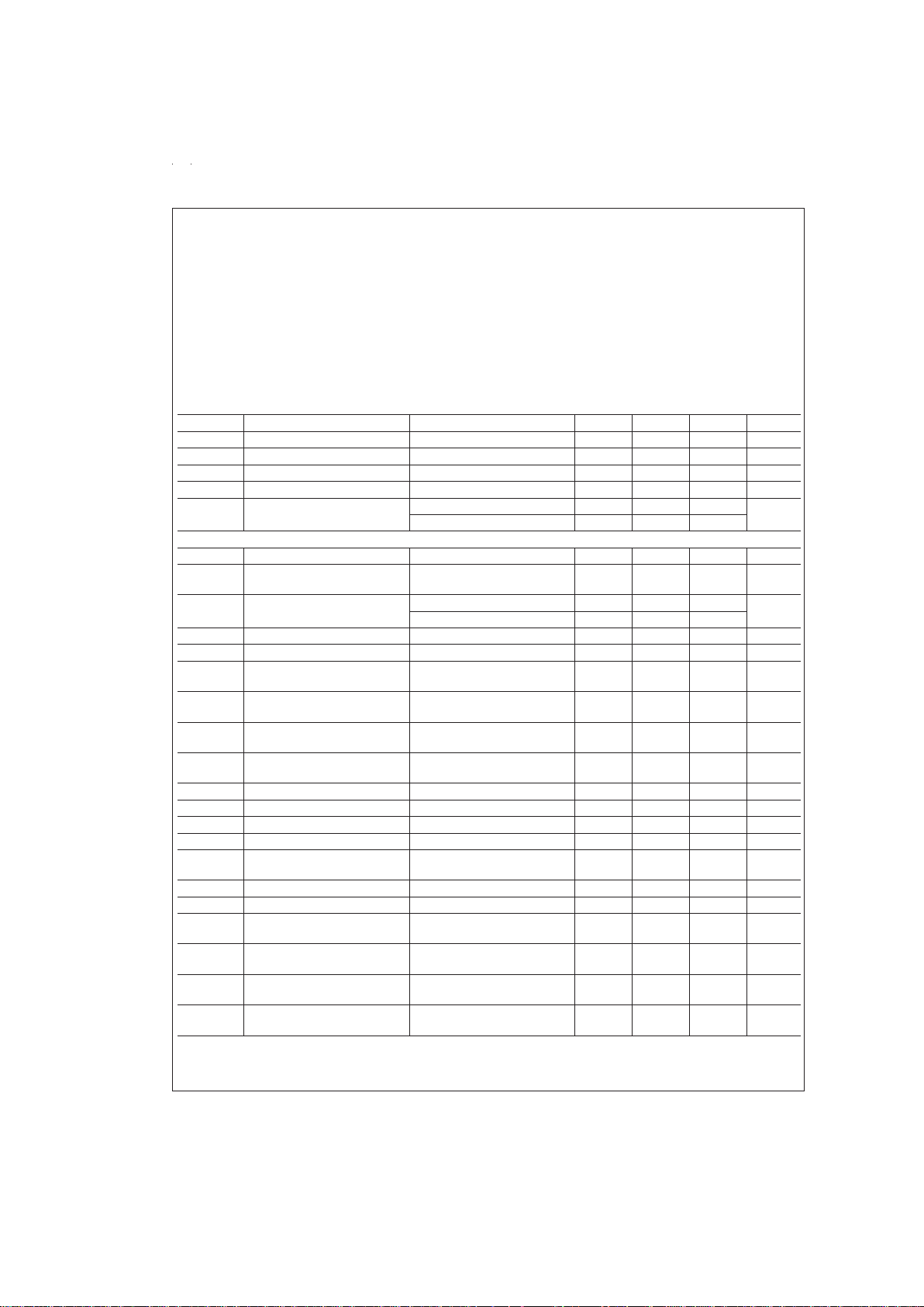
TABLE 1. 5-Bit DAC Output Voltage Table
(V
CC
=
5V, V
DD
=
12V
±
5%,T
A
=
25˚C, Test Mode)
Symbol Parameter Conditions Typical Units
V
DACOUT
5-Bit DAC Output Voltages for Different VID Codes VID4:0=01111
1.30
V
VID4:0=01110 1.35
VID4:0=01101
1.40
VID4:0=01100 1.45
VID4:0=01011
1.50
VID4:0=01010
1.55
VID4:0=01001
1.60
VID4:0=01000 1.65
VID4:0=00111
1.70
VID4:0=00110 1.75
VID4:0=00101
1.80
VID4:0=00100 1.85
VID4:0=00011
1.90
VID4:0=00010 1.95
VID4:0=00001
2.00
VID4:0=00000 2.05
VID4:0=11111 (shutdown)
VID4:0=11110 2.1
VID4:0=11101
2.2
VID4:0=11100 2.3
VID4:0=11011 2.4
VID4:0=11010 2.5
VID4:0=11001 2.6
VID4:0=11000 2.7
VID4:0=10111
2.8
VID4:0=10110 2.9
VID4:0=10101 3.0
VID4:0=10100 3.1
VID4:0=10011 3.2
VID4:0=10010
3.3
VID4:0=10001 3.4
VID4:0=10000 3.5
www.national.com 4
Page 5

Pin Description
Pin Pin Name Pin Function
1 LG Low side N-FET gate driver output.
2 PGND Ground for the two FET drivers of the switching section.
3V
DD
Supply for the FET gate drivers. Usually tied to +12V.
4 SNS2 Feedback pin for the 1.5V linear regulator.
5 G2 Gate drive output for the external N-MOS of the fast 1.5V linear regulator.
6 SGND Ground for internal signal circuitry and system ground reference.
7V
CC
Supply voltage. Usually +5V.
8 SNS1 Output voltage monitor input for the switching regulator.
9 CS+ Switching regulator current sense input, positive node.
10 CS− Switching regulator current sense input, negative node.
11 CP Charge pump. Output is a square wave with 50%duty cycle. Amplitude is close to V
CC
voltage.
12 FREQ Switching frequency adjustment pin. An external resistor is needed to set the desired
frequency.
13 EAO Output of the error amplifier. Used for compensating the switching regulator.
14 FB Inverting input of the error amplifier. Used for compensating the switching regulator.
15 PWGD Open collector Power Good signal.
16 VID4 5-Bit DAC input, MSB.
17 VID3 5-Bit DAC input.
18 VID2 5-Bit DAC input.
19 VID1 5-Bit DAC input.
20 VID0 5-Bit DAC input, LSB.
21 G3 Gate drive pin for the external N-MOS of the 1.25V linear regulator.
22 SNS3 Feedback pin for the 1.25V linear regulator.
23 EN Output Enable. A logic low shuts the whole chip down.
24 HG High side N-FET gate driver output.
www.national.com5
Page 6

Block Diagram
Test Circuit
DS101034-3
DS101034-4
FIGURE 1. LDO Controller Test Circuit
www.national.com 6
Page 7

Typical Application
DS101034-2
FIGURE 2. Using LM2638 to Supply GTL+ Bus (VTT, 1.5V, 5.6A), 2.5V Standby (V
CC
2_5SBY, 2A Full Power and 180 mA Suspend) and
3.3V Standby (V
CC
3_3SBY, 1.5A Full Power, 0.5A Suspend)
www.national.com7
Page 8

Physical Dimensions inches (millimeters) unless otherwise noted
LIFE SUPPORT POLICY
NATIONAL’S PRODUCTS ARE NOT AUTHORIZED FOR USE AS CRITICAL COMPONENTS IN LIFE SUPPORT
DEVICES OR SYSTEMS WITHOUT THE EXPRESS WRITTEN APPROVAL OF THE PRESIDENT AND GENERAL
COUNSEL OF NATIONAL SEMICONDUCTOR CORPORATION. As used herein:
1. Life support devices or systems are devices or
systems which, (a) are intended for surgical implant
into the body, or (b) support or sustain life, and
whose failure to perform when properly used in
accordance with instructions for use provided in the
labeling, can be reasonably expected to result in a
significant injury to the user.
2. A critical component is any component of a life
support device or system whose failure to perform
can be reasonably expected to cause the failure of
the life support device or system, or to affect its
safety or effectiveness.
National Semiconductor
Corporation
Americas
Tel: 1-800-272-9959
Fax: 1-800-737-7018
Email: support@nsc.com
National Semiconductor
Europe
Fax: +49 (0) 1 80-530 85 86
Email: europe.support@nsc.com
Deutsch Tel: +49 (0) 1 80-530 85 85
English Tel: +49 (0) 1 80-532 78 32
Français Tel: +49 (0) 1 80-532 93 58
Italiano Tel: +49 (0) 1 80-534 16 80
National Semiconductor
Asia Pacific Customer
Response Group
Tel: 65-2544466
Fax: 65-2504466
Email: sea.support@nsc.com
National Semiconductor
Japan Ltd.
Tel: 81-3-5639-7560
Fax: 81-3-5639-7507
www.national.com
24-Lead Small Outline Package
Order Number LM2638M
NS Package Number M24B
LM2638 Motherboard Power Supply Solution with a 5-Bit Programmable Switching Controller and
Two Linear Regulator Controllers
National does not assume any responsibility for use of any circuitry described, no circuit patent licenses are implied and National reserves the right at any time without notice to change said circuitry and specifications.
 Loading...