

Page 1
LM2637
Motherboard Power Supply Solution with a 5-Bit
Programmable Switching Controller and Two Linear
Regulator Controllers
General Description
The LM2637 provides a comprehensive embedded power
supply solution for motherboards hosting high performance
MPUs such as M II
™
, Pentium™II, K6-2 and other similar
high performance MPUs. The LM2637 incorporates a 5-bit
programmable, synchronous buck switching controller and
two high-speed linear regulator controllers in a 24-pin SO
package.
Switching Section
— The switching regulator controller features a 5-bit programmable DAC, over-current and
over-voltage protection, under-voltage latch-off, a power
good signal, and output enable. The 5-bit DAC has a typical
tolerance of 1%. There are two user-selectable over-current
protection methods. One provides accurate over-current protection with the use of an external sense resistor. The other
saves cost by taking advantage of the r
DS_ON
of the
high-side FET.The over voltage protection provides two levels of protection. The first level keeps the high-side FET off
and the low-side FET on. The second provides a gate signal
that can be used to fire an external SCR.
Linear Section
— The two linear regulator controllers feature wide control bandwidth, N-FET and NPN transistor driving capability, and an adjustable output voltage. The wide
control bandwidth makes meeting fast load transient response requirement such as that of the GTL+ bus an easy
job. In minimum configuration, the two controllers default to
1.5V and 2.5V respectively.
Both linear controllers have under voltage latch-off.
Features
n Provides 3 regulated voltages
n Power Good flag and output enable
n Under-voltage latch-off
Switching Section
n Synchronous rectification
n 5-bit DAC programmable from 3.5V to 1.3V
n Typical 1%DAC tolerance
n Switching frequency: 50 kHz to 1 MHz
n Two levels of over-voltage protection
n Two methods of over-current protection
n Adaptive non-overlapping FET gate drives
n Soft start without external capacitor
Linear Section
n N-FET and NPN driving capability
n Ultra fast response speed
n Output voltages default to 1.5V and 2.5V yet adjustable
Applications
n Embedded power supplies for PC motherboards
n Triple DC/DC power supplies
n Programmable high current DC/DC power supply
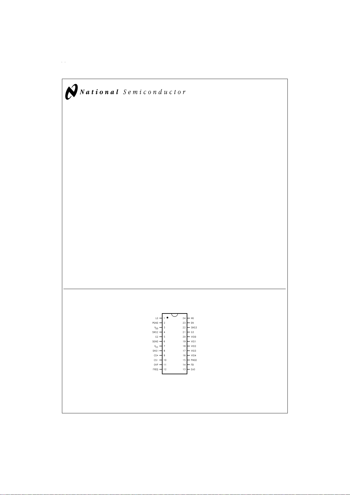
Pin Configuration
MII™is a trademark of CyrixCorporation a wholly owned subsidiary of National Semiconductor Corporation.
Pentium
™
is a trademark of Intel Corporation.
K6 is trademark of Advanced Micro Devices, Inc.
24-Lead SOIC
DS100848-1
Top View
NS Package Number M24B
October 1998
LM2637 Motherboard Power Supply Solution with a 5-Bit Programmable Switching Controller and
Two Linear Regulator Controllers
© 1999 National Semiconductor Corporation DS100848 www.national.com
Page 2
Absolute Maximum Ratings (Note 1)
If Military/Aerospace specified devices are required,
please contact the National Semiconductor Sales Office/
Distributors for availability and specifications.
V
CC
7V
V
DD
17V
Junction Temperature 150˚C
Power Dissipation (Note 2) 1.6W
Storage Temperature −65˚C to +150˚C
ESD Susceptibility 2.5 kV
Soldering Time, Temperature (10 sec.) 300˚C
Operating Ratings (Note 1)
V
CC
4.75V to 5.25V
Junction Temperature Range 0˚C to +125˚C
Electrical Characteristics
V
CC
=
5V, V
DD
=
12V unless otherwise specified. Typicals and limits appearing in plain type apply for T
A
=
T
J
=
+25˚C. Limits
appearing in boldface type apply over the 0˚C to +70˚C range.
Symbol Parameter Conditions Min Typ Max Units
I
EN
EN Pin internal Pull-Up Current 60 90 140 µA
I
VID
VID Pins internal Pull-Up
Current
60 90 140 µA
I
CC
Operating VCCCurrent EN=5V, VID=10111 6 7.5 mA
I
Q_VCC
VCCShutdown Current EN=0V, VID Pins Floating 1.5 3 mA
SWITCHING SECTION
V
DACOUT
5-Bit DAC Output Voltage (Note 3)
N
−1.5
%
NN
+1.5
%
V
I
Q_VDD
VDDShutdown Current EN=0V, VID Pins Floating 4 µA
f
OSC
Oscillator Frequency RT=100 kΩ 204 245 286
kHz
RT=25 kΩ 1000
D
MAX
Maximum Duty Cycle 95
%
D
MIN
Minimum Duty Cycle 0
%
R
SNS1
SNS1 Pin Resistance to
Ground
8.5 10 13 kΩ
R
DS_SRC
Gate Driver Resistance When
Sourcing Current
6 Ω
R
DS_SINK
Gate Driver Resistance When
Sinking Current
1.5 Ω
V
CC_TH1
Rising VCCThreshold for
Power-On Reset
4 4.3 V
V
CC_TH2
Falling VCCThreshold for
Power-On Reset
3.0 3.6 V
V
DAC_IH
DAC Input High Voltage 3.5 V
V
DAC_IL
DAC Input Low Voltage 1.3 V
t
PWGD
PWGD Response Time SNS1 Rises from 0V to Rated
Output Voltage
2 8.4 15 µs
t
PWBAD
PWGD Response Time SNS1 Falls from Rated Output
Voltage to 0V
2 3.4 10 µs
V
PWGD_HI
PWGD High Trip Point
%
Above Rated Output Voltage
when output Voltage
↑
11.5 13
%
%
Above Rated Output Voltage
when output Voltage
↓
(Note 4)
5 7 9
V
PWGD_LO
PWGD Low Trip Point
%
Below Rated Output Voltage
when output Voltage
↑
2.6 6
%
%
Below Rated Output Voltage
when output Voltage
↓
(Note 4)
6 9.5 13
V
OVP_TRP
OVP Pin Trip Point
%
SNS1 Above Rated Output 15 18 21
%
I
CS+
CS+ Pin Sink Current CS+=5V 126 185 244 µA
V
OCP
Over-Current Trip Point (CS+
and CS− Differential Voltage)
CS+=2V, CS− Drops from 2V
41 55 69 mV
www.national.com 2
Page 3
Electrical Characteristics (Continued)
V
CC
=
5V, V
DD
=
12V unless otherwise specified. Typicals and limits appearing in plain type apply for T
A
=
T
J
=
+25˚C. Limits
appearing in boldface type apply over the 0˚C to +70˚C range.
Symbol Parameter Conditions Min Typ Max Units
SWITCHING SECTION
I
OVP
OVP Pin Source Current OVP=3V 10 mA
GA Error Amplifier DC Gain 76 dB
B
WEA
Error Amplifier Unity Gain
Bandwidth
5 MHz
V
RAMP_L
Ramp Signal Valley Voltage 1.25 V
V
RAMP_H
Ramp Signal Peak Voltage 3.25 V
t
SS
Soft Start Time
4096
Clock
Cycles
D
STEP_SS
Duty Cycle Step Change in
Soft Start
12.5
%
1.5V LDO CONTROLLER SECTION
V
SNS2
SNS2 Voltage V
DD
=
12V, V
CC
=
4.75V to
5.25V, I
G2
=
0mAto20mA
(
Figure 1
)
1.463 1.5 1.538 V
R
OUT2
Output Resistance 200 Ω
I
SNS2
SNS2 Pin Bias Current When Regulating 21 µA
V
PWGD_HI
PWGD High Trip Point (Note 4) 0.63 V
V
PWGD_LO
PWGD Low Trip Point (Note 4) 0.44 V
2.5V LDO CONTROLLER SECTION
V
SNS3
SNS3 Voltage V
DD
=
12V, V
CC
=
4.75V to
5.25V, I
G3
=
0mAto20mA
(
Figure 1
)
2.438 2.5 2.563 V
R
OUT3
Output Resistance 200 Ω
I
SNS3
SNS3 Pin Bias Current When Regulating 21 µA
V
PWGD_HI
PWGD High Trip Point (Note 4) 0.63 V
V
PWGD_LO
PWGD Low Trip Point (Note 4) 0.44 V
Note 1: Absolute Maximum Ratings are limits beyond which damage to the device may occur. Operating ratings are conditions under which the device operates
correctly. Operating Ratings do not imply guaranteed performance limits.
Note 2: Maximum allowable power dissipation is a function of the maximum junction temperature, T
JMAX
, the junction-to-ambient thermal resistance, θJA, and the
ambient temperature, T
A
. The maximum allowable power dissipation at any ambient temperature is calculated using:
P
MAX
=
(T
JMAX−TA
)/
θ
JA
.
The
junction-to-ambient thermal resistance, θ
JA
, for LM2637 is 78˚C/W. For a T
JMAX
of 150˚C and TAof 25˚C, the maximum allowable power dissipation is 1.6W.
Note 3: The letter
N
stands for the typical output voltages appearing in
italic boldface
type in
Table 1
.
Note 4: The output level of the PWGD pin is a logic AND of the power good function of the switching section, the 1.5V section and the 2.5V section.
www.national.com3
Page 4
Electrical Characteristics (Continued)
TABLE 1. 5-Bit DAC Output Voltage Table
(V
CC
=
5V, V
DD
=
12V
±
5%,T
A
=
25˚C, Test Mode)
Symbol Parameter Conditions Typical Units
V
DACOUT
5-Bit DAC Output Voltages for Different VID Codes VID4:0=01111
1.30
V
VID4:0=01110 1.35
VID4:0=01101
1.40
VID4:0=01100 1.45
VID4:0=01011
1.50
VID4:0=01010 1.55
VID4:0=01001
1.60
VID4:0=01000 1.65
VID4:0=00111
1.70
VID4:0=00110 1.75
VID4:0=00101
1.80
VID4:0=00100 1.85
VID4:0=00011
1.90
VID4:0=00010 1.95
VID4:0=00001
2.00
VID4:0=00000 2.05
VID4:0=11111 (shutdown)
VID4:0=11110 2.1
VID4:0=11101
2.2
VID4:0=11100 2.3
VID4:0=11011 2.4
VID4:0=11010 2.5
VID4:0=11001 2.6
VID4:0=11000 2.7
VID4:0=10111
2.8
VID4:0=10110 2.9
VID4:0=10101 3.0
VID4:0=10100 3.1
VID4:0=10011 3.2
VID4:0=10010
3.3
VID4:0=10001 3.4
VID4:0=10000 3.5
www.national.com 4
Page 5
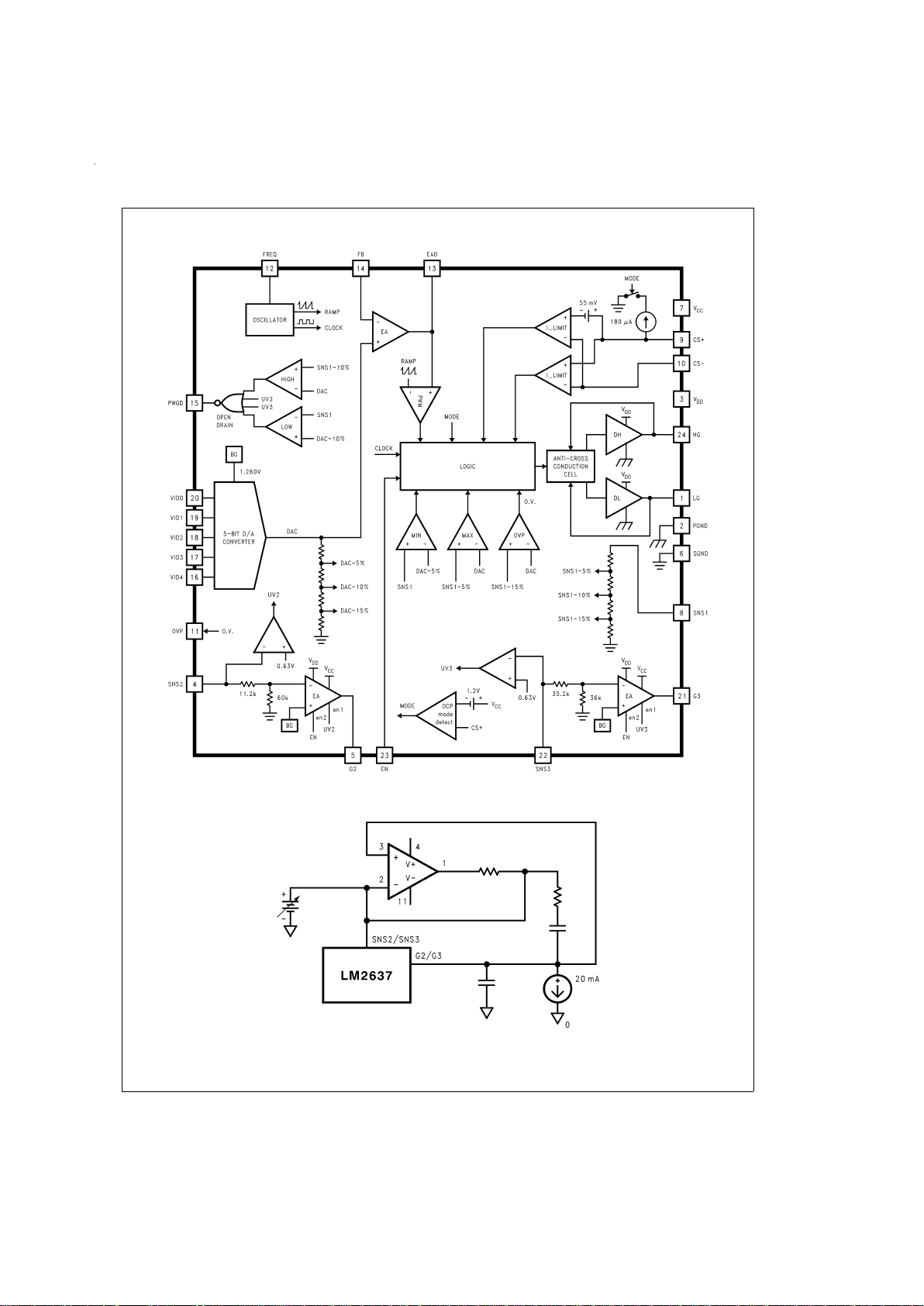
Block Diagram
Test Circuit
DS100848-30
DS100848-2
FIGURE 1. LDO Controller Test Circuit
www.national.com5
Page 6
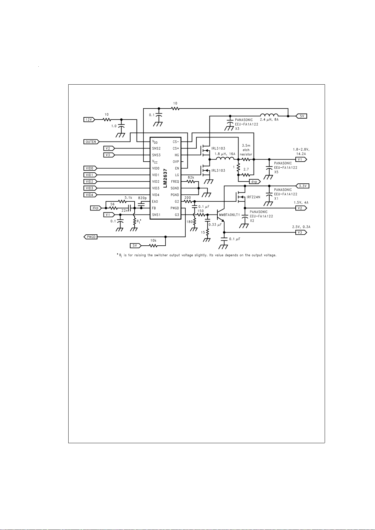
Typical Applications
DS100848-3
FIGURE 2. Motherboard Power Supply for Pentium II Processor Core (1.3V - 2.8V, 14.2A), GTL+ Bus (1.5V, 4A), and
Legacy I/O (2.5V, 0.3A). External sense resistor is used to provide both over-current limit and dynamic voltage
positioning.
www.national.com 6
Page 7

Typical Applications (Continued)
DS100848-4
FIGURE 3. Motherboard Power Supply for Pentium II Processor Core (1.8V - 2.8V, 14.2A), GTL+ Bus (1.5V, 4A), and
Legacy I/O (2.5V, 0.3A). High side FET is used to provide the current limit.
www.national.com7
Page 8

Pin Description
Pin Pin Name Pin Function
1 LG Low side N-FET gate driver output.
2 PGND Ground for the two FET drivers of the switching section.
3V
DD
Supply for the FET gate drivers. Usually tied to +12V.
4 SNS2 Feedback pin for the 1.5V linear regulator.
5 G2 Gate drive output for the external N-MOS of the fast 1.5V linear regulator.
6 SGND Ground for internal signal circuitry and system ground reference.
7V
CC
Supply voltage. Usually +5V.
8 SNS1 Output voltage monitor input for the switching regulator.
9 CS+ Switching regulator current sense input, positive node.
10 CS− Switching regulator current sense input, negative node.
11 OVP Over-voltage protection output for the switching regulator. Can be used to fire an external
SCR.
12 FREQ Switching frequency adjustment pin. An external resistor is needed to set the desired
frequency.
13 EAO Output of the error amplifier. Used for compensating the switching regulator.
14 FB Inverting input of the error amplifier. Used for compensating the switching regulator.
15 PWGD Open collector Power Good signal.
16 VID4 5-Bit DAC input, MSB.
17 VID3 5-Bit DAC input.
18 VID2 5-Bit DAC input.
19 VID1 5-Bit DAC input.
20 VID0 5-Bit DAC input, LSB.
21 G3 Gate drive pin for the external N-MOS of the 2.5V linear regulator.
22 SNS3 Feedback pin for the 2.5V linear regulator.
23 EN Output Enable. A logic low shuts the whole chip down.
24 HG High side N-FET gate driver output.
Applications Information
OVERVIEW
The LM2637 provides control and protection for three voltage regulators. Namely, a synchronous buck switching controller and two linear regulator controllers that drive an external N-FET or NPN transistor.
Switching Section
—The switching controller features a
VRM-compatible, 5-bit programmable output voltage,
over-current and over-voltage protection, under-voltage
latch-off, a power good signal, and an output enable. The
5-bit DAC has a typical tolerance of 1%. There are two
user-selectable over-current protection methods. One provides accurate over-current protection with the use of an external sense resistor. The other saves cost by taking advantage of the r
DS_ON
of the high-side FET. The over-voltage
protection provides two levels of protection. The first turns off
the high-side FET and turns on the low-side. The second
provides a gate signal that can be used to fire an external
SCR.
The PWM frequency is adjustable from 50 kHz to beyond 1
MHz through an external resistor.
Soft start is realized through an internal digital counter. No
external soft start capacitor is necessary.
Dynamic positioning of the switcher output voltage reduces
the number of output capacitors and can be easily realized
using the same sense resistor as the over-current protection.
Linear Section
—The two linear regulator controllers feature
wide control bandwidth, N-FET and NPN transistor driving
capability, an adjustable output voltage and a typical 2%tolerance. The wide control bandwidth makes meeting the
GTL+ bus transient response requirement an easy job.
When no external resistor divider is used, the two controllers
default to 1.5V and 2.5V respectively.
Both linear sections have under-voltage latch-off. Should the
output voltage drop below 0.63V, the corresponding gate
drive will be disabled and PWGD pin will be pulled low.
THEORY OF OPERATION
Start Up
Switching Section
—The soft start circuitry starts to work
when three conditions are met, i.e., EN pin is a logic high, the
VID code is valid and V
CC
pin voltage exceeds 4.2V.The duration of the soft start is determined by an internal digital
counter and the switching frequency. During soft start, the
output of the error amplifier is allowed to increase gradually.
When the counter has counted 4,096 clock cycles, soft start
session ends and the output level of the error amplifier is released and allowed to go to a value that is determined by the
feedback loop. PWRGD pin is always low during soft start
and is turned over to output voltage monitoring circuitry after
that. Before V
CC
reaches 4V, all internal logic is in a
power-on-reset state and the two FET drivers are disabled.
www.national.com 8
Page 9

Applications Information (Continued)
During normal operation, if V
CC
voltage drops below 3.6V,
the internal circuitry will go into power-on-reset again. The
hysteresis helps decrease the noise sensitivity on the V
CC
pin.
After soft start ends and during normal operation, if the con-
verter output voltage exceeds 118%of DAC output voltage,
the LM2637 will lock into over-voltage protection mode. The
high-side drive will be low,and the low-side drive will be high.
There are two ways to clear the mode. One is to cycle V
CC
voltage once. The other is to toggle the EN level. After the
over-voltage protection mode is cleared, the LM2637 will enter the soft start session and start over.
Linear Section
—The linear section does not go through a
soft start. Whenever the soft start of the switching section
begins, the linear section immediately applies the required
gate voltages or base currents for external power transistors.
There is an under-voltage latch-off for the linear section. If
after soft start ends, SNS2 or SNS3 is below 0.63V, the corresponding gate drive will be disabled and PWGD pin will be
pulled low.
Normal Operation
Switching Section
—In the normal operation mode, the
LM2637 regulates the converter output voltage by adjusting
the duty ratio. The output voltage is determined by the 5-bit
VID code set by the user or MPU.
The PWM frequency is set by an external resistor between
FREQ pin and ground. The resistance needed for a desired
PWM frequency can be determined by the following equation:
(1)
For example, if the desired PWM frequency is 300 kHz, the
resistance should be around 84 kΩ.
The minimum allowable PWM frequency is 5 kHz.
Linear Section
—Under steady state operation, the linear
section supplies the appropriate gate voltage or base current
to correctly bias the external pass transistor so that the voltage drop across the transistor is the right value.
Resetting the LM2637
When the LM2637 detects an abnormal condition such as
switching regulator over voltage, it will latch itself off partially
or completely.Toreset the LM2637, either EN or V
CC
voltage
has to be toggled. Another more subtle way to recover is to
float all the VID pins and reapply the correct code.
Gate Drives
Switching Section
—The switching controller has two gate
drives that are suitable for driving external power N-FETs in
a synchronous buck topology. The voltage for the two FET
drivers is supplied by the V
DD
pin. This VDDvoltage should
be at least one V
GS
(th) higher than converter input voltage to
be able to fully enhance the high-side FET. In a typical PC
motherboard application, it is recommended that 12V be applied to V
DD
, and 5V be used as the input voltage for the
switcher. A charge pump is not recommended since the linear sections need a stable V
DD
voltage to minimize high fre-
quency noise.
ForaV
DD
of 12V, the peak gate charging current is typically
2A, and the peak gate discharging current is typically 6A,
well suited for high speed switching.
The LM2637 gate drives are of BiCMOS design. Unlike
some bipolar control ICs, the gate drive has rail-to-rail swing
that ensures no spurious turn-on due to capacitive coupling.
Another feature of the FET gate drives is the adaptive
non-overlapping mechanism. A gate drive is not turned on
until the other is fully off. The dead time in between is typically 20 ns. This avoids the potential shoot-through problem
and helps improve efficiency.
Linear Section
—The gate drives of the linear section can
put out a maximum continuous current of about 40 mA. The
typical low gate voltage is 1.2V.
Load Transient Response
Switching Section
—In a typical modern MPU application
such as the M II, Pentium II and K6-2 core power supply,
load transient response is a critical issue. The LM2637 utilizes the conventional voltage feedback technology as the
primary feedback control method. When the load transient
happens, the error in the output voltage level is fed to the error amplifier. The output of the error amplifier is then compared with an internally generated PWM ramp signal and the
result of the comparison is a series of pulses with certain
duty ratios. These pulses are then used to control the on and
off of the FET gate drives. In this way, the error in the output
voltage gets corrected by the change in the duty ratio of the
FET switches. During a large load transient, depending on
the compensation design, the change in duty ratio usually
begins within one switching cycle. Refer to the
Design Con-
siderations
section for more details.
Besides the voltage feedback control loop, the LM2637 also
has a pair of fast comparators (the MIN and MAX comparators) to help maintain the output voltage during a large and
fast load transient. The trip points of the comparators are set
to
±
5%of the DAC output voltage. When the load transient
is so large that the output voltage goes outside the
±
5%window, the MIN or MAX comparator will bypass the primary
voltage control loop and immediately set the duty ratio to either 100%or 0%. This provides the fastest possible way to
react to such a large load transient in a conventional buck
converter.
Linear Section
—The linear section has a high control bandwidth. Depending on external components selected, the typical bandwidth can be as high as 1.2 MHz. The user may
choose to lower this bandwidth and have a better noise immunity by adding a small capacitor (1 nF to 10 nF) between
the gate output and ground.
Power Good Signal
The power good signal is to indicate whether all three output
voltages are within their corresponding range. The range for
the switching regulator is set to a typical
±
10%window of the
DAC output voltage. The range for the linear regulator is
0.63V to infinity. During soft start, the power good signal is
kept low. At the completion of soft start, all three output voltages are checked and the PWGD pin will be asserted if they
are all within specified range. During normal operation,
whenever a voltage goes out of the specified range for more
than about 3 µs, PWGD pin will be pulled low.
Over-Voltage Protection
Switching Section
—When the output voltage exceeds
118%of the DAC output voltage any time beyond the soft
start, the switching section will enter over-voltage protection
mode and shuts itself down. The upper gate drive will be
held low while the lower gate drive will be held high. PWGD
www.national.com9
Page 10

Applications Information (Continued)
will be low. There will also be a logic high signal at the OVP
pin that can be used to fire an external SCR. To clear this
mode, refer to the
Resetting the LM2637
section.
Linear Section
—There is no over-voltage protection in the
linear controllers.
Under-Voltage Latch-Off
At the completion of soft start, the controller starts to monitor
all three output voltages. If any of the voltages goes below
about 0.63V, the controller will latch off its corresponding
section, i.e., switching or linear. The mode can be cleared by
following the procedures described in the
Resetting the
LM2637
section.
Current Limit
Switching Section
—Current limit can be realized by two
methods. One method is through sensing the V
DS
of the
high-side FET. The other is through a separate sense resistor.The first method is cheaper and more power efficient but
less accurate. The second method is more accurate but dissipates additional power and is either more expensive or requires special PCB layout consideration. A side benefit of the
second method is it enables implementation of a technique
called dynamic voltage positioning, which helps save the
number of output capacitors.
The LM2637 tells in which current limit mode it is supposed
to be by detecting the CS+ pin voltage. When CS+ voltage is
1.2V below V
CC
voltage, sense resistor method is assumed.
Otherwise the V
DS
method is chosen. The VDSmethod is
based on typical r
DS_ON
of the high-side FET and load cur-
rent levels.
Method 1—High-Side FET VDSSensing
This method detects the high-side FET drain current by
sensing its drain-source voltage when it is on. See
Figure 4
.
Since the r
DS_ON
of a FET is a known value, current through
the FET can be known by measuring its V
DS
. The relation-
ship between the three parameters is:
(2)
To implement the current limit function, an external resistor
R
IMAX
is needed. The resistor should be connected between
the drain of the high-side FET and IMAX pin. A constant current of around 180 µA is forced to flow into the IMAX pin and
causes a fixed voltage drop across the R
IMAX
resistor. This
voltage drop is then compared with the V
DS
of the high-side
FET and if the latter is higher, over current is assumed. The
appropriate value of R
IMAX
for a pre-determined current limit
level I
LIM
can be determined by the following equation:
(3)
For example, suppose that the r
DS_ON
of the FET is 20 mΩ,
and the desired current limit is 20A, then R
IMAX
should be
2.2 kΩ.
Notice however, that the r
DS_ON
of the FET has a positive
temperature coefficient and it can increase by as much as
50%when heated up. Also the distribution of the r
DS_ON
can
be fairly wide, a 1.25 to 1.5 ratio is not uncommon. Consult
the MOSFET vendor for further information on the distribution of r
DS_ON
.
The designer should carefully choose the value of R
IMAX
so
that even under the extreme case (largest r
DS_ON
and highest temperature) the current limit will not trigger below the
preset value.
To provide the greatest protection over the high-side FET,
cycle-by-cycle protection is implemented. The sampling of
the V
DS
starts as early as 250 ns after the FET is turned on.
Whenever an over-current condition is detected, the
high-side FET is immediately turned off and the low-side
FET turned on. This status remains for the rest of the cycle.
The same procedure applies to the next switching cycle. The
blanking time of 250 ns is to avoid the switching noise that
occurs whenever the FET is turned on.
The resistor between CS− pin and the switching node
(source of the high-side FET) is important for minimizing the
noise and negative voltage present at the CS− pin. A resistance of 100Ω to 300Ω is recommended.
Method 2—Current Sense Resistor
This method uses a sense resistor in series with the output
inductor to detect the load current.
SeeFigure 5
. The voltage
across the sense resistor is proportional to load current. In
the case that the sense resistor is of discrete type (i.e., not a
PCB etch resistor) or the sense resistor value is optimized
for dynamic voltage positioning (see the
Dynamic Position-
ing of Load Voltage
section), it may be necessary to use two
signal level resistors, R
1
and R2to appropriately set the de-
sired current limit.
DS100848-8
FIGURE 4. Current Limit via High-Side FET V
DS
Sensing
www.national.com 10
Page 11

Applications Information (Continued)
For a given current limit value, the minimum R
SENSE
is deter-
mined by:
(4)
where V
OCP
is the over-current trip voltage and is typically
55 mV, see the
Electrical Characteristic
table. For example,
for a 20Acurrent limit, the minimum R
SENSE
is 2.75 mΩ.Ifa
3mΩsense resistor is used instead, use appropriate values
of R
1
and R2to make the voltage across R1to be V
OCP
when
the voltage across R
SENSE
is 60 mV.
The discrete current sense resistor usually has a very good
temperature coefficient and tolerance. A temperature coefficient of
±
30 ppm/˚C is typical. Tolerance is usually±1%or
±
5%. Vishay Dale and IRC offer a broad range of discrete
sense resistors.
A PCB etch resistor can also be used as the R
SENSE
. The
advantage of that approach is flexible resistance, which will
result in minimum power loss. R
1
and R2may also be eliminated. The drawback is too high a temperature coefficient,
typically +4000 ppm/˚C, which will result in a much less accurate current limit than a discrete sense resistor. The copper thickness of a PCB is usually of 5%tolerance.
Linear Section
—There is no current limit function in the linear controllers. However, if there is ever a severe over-load,
the output voltage may drop below 0.63V, in which case the
under-voltage latch-off will provide the protection.
DESIGN CONSIDERATIONS
Control Loop Compensation
Switching Section
—A switching regulator should be properly compensated to achieve a stable operation, tight regulation and good dynamic performance. For a synchronous
buck regulator that needs to meet stringent load transient requirement such as that of processor core voltage supply, a
2-pole-1-zero compensation network should suffice, such as
the one shown in
Figure 6
(C1,C2,R1and R2). This is because the ESR zero of the typical output capacitors is low
enough to make the control-to-output transfer function a
single-pole roll-off.
As an example, let us figure out the values of the compensation network components in
Figure 6
. Assume the following
parameters: R=20Ω,R
L
=
20 mΩ,R
C
=
9mΩ,L=2 µH, C
=
7.5 mF, V
IN
=
5V,V
m
=
2V and PWM frequency=300 kHz.
Notice R
L
is the sum of the inductor DC resistance and the
on resistance of the FET’s.
The control-to-output transfer function is:
(5)
The ESR zero frequency is:
(6)
The double pole frequency is:
(7)
The corresponding Bode plots are shown in
Figure 7
.
Notice since the ESR zero frequency is so low that the phase
doesn’t even go beyond −90˚. This makes the compensation
easier to do.
Since the DC gain and cutoff frequency (0 dB frequency) are
too low, some compensation is needed. Otherwise the low
DC gain will cause a poor line regulation, and the low cutoff
frequency may hurt transient response performance.
The transfer function for the 2-pole-1-zero compensation
network shown in
Figure 6
is:
(8)
where
(9)
One of the poles is located at origin to help achieve the highest DC gain. So there are three parameters to determine, the
position of the zero, the position of the second pole, and the
constant A. To determine the cutoff frequency and phase
margin, the loop bode plots need to be generated. The loop
transfer function is:
TF=−TF1 x TF2 (10)
By choosing the zero close to the double pole position and
the second pole to half of the switching frequency, the closed
loop transfer function turns out to be very good.
DS100848-9
FIGURE 5. Current Limit via Current Sense Resistor
www.national.com11
Page 12

Applications Information (Continued)
That is, if f
z
=
1.32 kHz, f
p
=
153 kHz, and A=4.8x10
−6
ΩF,
then the cutoff frequency will be 50 kHz, the phase margin
will be 72˚, and the DC gain will be that of the error amplifier.
See
Figure 8
.
The compensation network component values can be determined by
Equation (9)
, since the values of fz,fpand A are
now known. To more conveniently calculate the values,
Equation (9)
can be rearranged as follows:
(11)
Notice there are three equations but four variables. So one
of the variables can be chosen arbitrarily. Since the current
driving capability of the error amplifier is limited to around 3
mA, it is a good idea to have a high impedance path from
EAO to FB. From
Equation (11)
it can be told that a larger R
2
will result in a smaller C1,C2and a larger R1. Calculations
show that the following combination is a good one: R
2
=
51Ω,C
1
=
0.022 µf, R
1
=
5.6 kΩ,C
2
=
820 pF.
For a different application or different type of output capacitors, a different compensation scheme may be necessary.
The user can either follow the steps above to figure the appropriate component values or contact National for help.
Linear Section
—The linear sectionis designed for high control bandwidth operation. The phase margin and cutoff frequency depends on the external N-FET, output capacitors
and their ESR. As a rule of thumb, the designer can choose
any capacitance from 50 µF to 4000 µF, with a total ESR of
10 mΩ to 100 mΩ. The larger the capacitance, the lower the
bandwidth. The above capacitors usually result in a control
bandwidth of 250 kHz to 1.2 MHz.
DS100848-17
FIGURE 6. Buck Converter from a Control Viewpoint
DS100848-18
FIGURE 7. Control-to-Output Bode Plots
DS100848-19
FIGURE 8. Loop Bode Plots
www.national.com 12
Page 13

Applications Information (Continued)
FET Selection
Switching Section
—The selection of FET switches affects
both the efficiency of the whole converter and the current
limit setting (if V
DS
sensing mode is selected). From efficiency standpoint it is suggested that for the high-side
switch, only logic level FETs be used. Standard FETscan be
used for the low-side switch when 12V is used to power the
V
DD
pin. The power loss associated with the FETs is
two-fold— Ohmic loss and switching loss. The Ohmic loss is
relatively easy to calculate whereas the switching loss is
much more difficult to estimate. The switching loss in a synchronous buck converter usually happens only in the
high-side FET. When the high-side FET starts to turn on, inductor current is flowing in the low-side body diode. Since
the body diode undergoes a reverse recovery before forced
off, the high-side FET will experience a pulse of drain current
turn on. The simultaneous presence of high drain-source
voltage and high drain current in the high-side FET causes
the switching loss. Apparently the switching loss is proportional to the PWM frequency.Having a Schottky diode in parallel with the low-side body diode will to a large extent alleviate the problem. This is because a Schottky diode does not
undergo a reverse recovery and it has a lower forward voltage than the body diode so it will take the majority of the inductor current after the low-side FET is turned off. The
low-side FET benefits from what is called zero voltage
switching (ZVS). That is because every time just before the
low-side FET is turned on, inductor current is already flowing
in its body diode, resulting in a low drain-source voltage.
When the low-side FET is turned off, current will be shifted to
its body diode temporarily, again clamping the drain-source
voltage to a low value.
It is difficult to calculate the switching loss due to its complicated nature. Fortunately at a reasonable PWM frequency
such as 300 kHz, the switching loss is usually much less
than the Ohmic loss. So the designer may initially ignore the
switching loss when trying to meet an efficiency specification.
The Ohmic loss for the high-side FET is:
(12)
The Ohmic loss for the low-side FET is:
(13)
Notice when determining the r
DS_ON
, the gate-source voltages are usually different for the two FET’s. For the
high-side FET, V
GS
is VDDminus drain voltage. For the
low-side, V
GS
is VDD. This means the low-side FET may
present a lower r
DS_ON
when the same type of FET is used
for both switches.
Since the r
DS_ON
has a positive temperature coefficient, the
actual Ohmic loss may be somewhat higher than calculated.
The power supply designer may target 125˚C FET operating
temperature under maximum load and highest ambient temperature and then use the corresponding r
DS_ON
found in the
FET datasheet.
Linear Section
—Two things need to be considered, i.e.,
r
DS_ON
and thermal capacity. Make sure that the maximum
possible r
DS_ON
on the N-FET is lower than the lowest
input-output differential voltage divided by maximum load
current. In a typical motherboard 3.3V to 1.5V or 3.3V to
2.5V application, this is not an issue because the maximum
allowable r
DS_ON
is way higher than a typical N-FET. It is the
thermal capacity and cost that limits the selection.As an example, consider a 3.3V to 1.5V, 4A application. The lowest
input-output differential voltage is 3.3V x 95%–1.5V x 102
%
=
1.605V,so the maximum allowable r
DS_ON
is 1.605V÷4A
=
401 mΩ. Almost all low voltage discrete N-FET’s can meet
this requirement. However, the maximum power dissipation
on the FET is (3.3V x 105%–1.5V x 98%)x4A=8W. At
least a TO-220 package with a beefy heat sink is necessary
to handle the thermal dissipation. When there is a load transient requirement such as that of the GTL+ supply, make
sure the r
DS_ON
is much lower than the value calculated from
steady state operation because headroom is important for
transient performance.
Capacitor Selection
Switching Section
—
Output Capacitors. The selection of capacitors is an extremely important step when designing a converter for a load
such as the MPU core. Since the typical slew rate of the load
current during a large load transient is around 20 A/µs to 30
A/µs, the switching converter has to rely on the output capacitors to take care of the first few microseconds. Under
such a current slew rate, ESR of the output capacitors is
more of a concern than the ESL in terms of voltage excursion. Depending on the kind of capacitors being used, total
output capacitance value may or may not be an important
factor.When the output capacitance is too low, the converter
may have to have a small output inductor to quickly supply
current to the output capacitors when the load suddenly
kicks in and to quickly stop supplying current when the load
is suddenly removed. Multilayer ceramic (MLC) capacitors
can have very low ESR but also a low capacitance value
compared to other kinds of capacitors. Low ESR aluminum
electrolytic capacitors tend to have large sizes and capacitance. Tantalum electrolytic capacitors can have a fairly low
ESR with a much smaller size and capacitance than the aluminum capacitors. Certain OSCON capacitors present ultra
low ESR and long life span. By the time the total ESR of the
output capacitor bank reaches around 9 mΩ, the capacitance of the aluminum/tantalum/OSCON capacitors is usually already in the millifarad range. For those capacitors,
ESR is the only factor to consider. MLCs can have the same
amount of total ESR with much less capacitance, most probably under 100 µF. A very small inductor, ultra fast control
loop and a high switching frequency become necessary in
such a case to deal with the fast charging/discharging rate of
the output capacitor bank.
From a cost savings standpoint, aluminum electrolytic capacitors are the most popular choice for output capacitors.
They have reasonably long life span and they tend to have
hugh capacitance to withstand the charging or discharging
process during a load transient for a fairly long period. Sanyo
MV-GX and MV-DX series’ give good performance when
enough of the capacitors are paralleled. The 6MV1500GX
capacitor has a typical ESR of 44 mΩ and a capacitance of
1500 µF at a voltage rating of 6.3V. For a detailed procedure
for determining number of output capacitors, refer to the application note
Using Dynamic Voltage Positioning Technique
to Reduce the Cost of Output Capacitors in Advanced Microprocessor Power Supplies
and the associated spreadsheet
for automated design.
Input Capacitors. The challenge on input capacitors is the
RMS ripple current. The large ripple current drawn by the
high-side switch tends to generate quite some heat due to
the capacitor ESR. The RMS ripple current ratings in the capacitor catalogs are usually specified under 105˚C. In the
www.national.com13
Page 14

Applications Information (Continued)
case of desktop PC applications, those ratings seem somewhat conservative.A rule-of-thumb is increase the 105˚C rating by 70%for desktop PC applications. The input RMS
ripple current value can be determined by the following
equation:
(14)
and the power loss in each input capacitor is:
(15)
In the case of 333 MHz Pentium II power supply, the maximum output current is around 14A. Under the worst case
when duty cycle is 50%, the maximum input capacitor RMS
ripple current is half of output current, i.e., 7A. Therefore
three Sanyo 16MV820GX capacitors are necessary under
room temperature (they are rated 1.45A at 105˚C). The
maximum ESR of those capacitors is 44 mΩ. So the maximum power loss in each of them is less than (7A)
2
x44
mΩ/3
2
=
0.24W. Note that the power loss in each capacitor
is inversely proportional to the square of the total number of
capacitors, which means the power loss in each capacitor
quickly drops when the number of capacitors increases.
Linear Section
—For applications where there is a load transient requirement such as that the GTL+ supply, low ESR capacitors should be considered. Make sure that the total ESR
multiplied by the maximum load current is smaller than half
the output voltage regulation window. The output voltage
regulation window should exclude the tolerance of LM2637.
For example, for a 3.3V to 1.5V, 2A design, the initial regulation window is
±
9%. Assume the tolerance of the LM2637
plus margin is
±
2%, then the effective window left is±7%or
±
105 mV. Therefore the ESR should be less than 105 mV
÷
2A=52 mΩ. A Sanyo 6MV1200DX is sufficient. For applications where the load is static and for control bandwidth and
stability issue, refer to the guidelines in the
control loop com-
pensation
section.
Inductor Selection
Output Inductor. The size of the output inductor is deter-
mined by a number of parameters. Basically the larger the
inductor, the smaller the output ripple voltage, but the slower
the converter’s response speed during a load transient. On
the other hand, a smaller inductor requires higher switching
frequency to maintain the same level of output ripple, and
probably results in a lossier converter, but has less inertia responding to load transient. In the case of MPU core power
supply, fast recovery of the load voltage from transient window back to the steady state window is important. That limits
the highest inductance value that can be used. The lowest
inductance value is limited by the highest switching frequency that can be practically employed. As the switching
frequency increases, the switching loss in the FETs tends to
increase, resulting in lower overall efficiency and larger heat
sinks. A good switching frequency is probably a frequency
under which the FET conduction loss is much higher than
the switching loss because the cost of the FET is directly related to its r
DS_ON
. The inductor size can be determined by
the following equation:
(16)
where V
o_rip
is the peak-peak output ripple voltage, f is the
switching frequency. For commonly used low r
DS_ON
FET’s,
a reasonable switching frequency is 300 kHz. Assume a
peak-peak output ripple voltage is 18 mV, the total output capacitor ESR is 9 mΩ, the input voltage is 5V, and output voltage is 2.8V, then the inductance value according to the
above equation will be 2 µH. The highest slew rate of the inductor current when the load changes from no load to full
load can be determined as follows:
(17)
where D
MAX
is the maximum allowed duty cycle, which is
around 0.95 for LM2637. For a load transient from 0A to 14A,
the highest current slew rate of the inductor, according to the
above equation, is 0.97 A/µs, and therefore the shortest possible total recovery time is 14A/(0.97 A/µs)=14.5 µs. Notice
that output voltage starts to recover whenever the inductor
starts to supply current.
The highest slew rate of the inductor current when the load
changes from full load to no load can be determined from the
same equation but use D
MIN
instead of D
MAX
.
Since the D
MIN
of LM2637 is at 0%, the slew rate is therefore
−1.4 A/µs. So the approximate total recovery time will be
14A/(1.4 A/µs)=10 µs.
Often times the power supply designer may have to use a
custom-made inductor for best performance/price ratio. Micrometals offers cost effective iron powder cores that are
widely adopted by motherboard supplies and OEMs. One
important rule when designing an iron power inductor is
never saturate the core or else it will exhibit extremely poor
dynamic performance. Useful inductor design tools can also
be found on their web page, www.micrometals.com. The
user of LM2637 can also contact National for a
custom-made inductor.
Alternatively the designer may use an open core inductor,
which is lower cost due to its ease of mass production. However, the open magnetic field may cause some noise problems to nearby circuitry and may cause EMI issues. However, no negative reports have been heard so far. Coilcraft
(www.coilcraft.com) offers a wide range of open core inductors. Custom-made parts are also possible. Other than
low cost, the advantages of open core inductors are less
board space and superior dynamic performance.
Input Inductor. The input inductor is for limiting the input
current slew rate during a load transient and normal operation. In the case that low ESR aluminum electrolytic capacitors are used for the input capacitor bank, input capacitor
voltage change due to capacitor charging/discharging is usually negligible for the first 20 µs. ESR is by far the dominant
factor in determining the amount of capacitor voltage
undershoot/overshoot during a fast load transient. So the
worst case is when the load changes between no load and
full load. Under that condition the input inductor sees the
highest voltage change across the input capacitors. Assume
the input capacitor bank consists of three 16MV820GX, i.e.,
a total ESR of 15 mΩ. Whenever there is a sudden load
change, the change in input current has to be initially supported by the input capacitor bank instead of the input inductor.So for a fast load-swing between 0A and 14A, the voltage
change seen by the input inductor is a ramp from 0V to a ∆V
or vice versa, whereas ∆V=14Ax15mΩ=210 mV.So this
situation is just as bad as operating under heaviest load. Use
the following equation to determine the minimum inductance
value:
www.national.com 14
Page 15

Applications Information (Continued)
(18)
where (di/dt)
max
is the maximum allowable input current slew
rate, which is 0.1 A/µs in the case of Pentium II power supply
and ∆V is equal to maximum load current times input capacitor ESR. So the input inductor size, according to the above
equation, should be 2.1 µH.
Dynamic Positioning of Load Voltage
The following is just a quick overview of a technique called
dynamic voltage positioning. For a detailed explanation and
examples please refer to our application note
Using Dynamic Voltage Positioning Technique to Reduce the Cost of
Output Capacitors in Advanced Microprocessor Power Supplies
. An associated spreadsheet is also available for auto-
mated design.
Since the typical MPU core voltage’s steady state regulation
window is fairly large, it is a good idea to dynamically position the steady state output voltage in the steady state regulation window with respect to load current level so that the
output voltage has more headroom for load transient response. This needs load current information. There are at
least two simple ways to implement this idea with LM2637.
One is to utilize the output inductor DC resistance, see
Fig-
ure 9
. The average voltage across the output inductor is actually that across its DC resistance, which is proportional to
load current.
Since the switching node voltage V
A
toggles between the input voltage and ground at the switching frequency, it is impossible to choose node A as the feedback point, otherwise
the dynamic performance will suffer and the system may
have noise problems. Using a low pass filter network around
the inductor, such as the one shown in the figure, seems to
be a good idea. The feedback point is node C.
Since at switching frequency the impedance of the 0.1 µF is
much less than 5 kΩ, so the toggling voltage at node A will
mainly drop across the 5 kΩ resistor and node C will be
much quieter than A. However, V
CB
average is still the ma-
jority of V
AB
average, because of the ratio of the resistor di-
vider.So in steady state V
C
=
I
OxrL+VCORE
, where rLis the
inductor DC resistance. So at no load, output voltage is
equal to V
C
, and at full load, output voltage is IOxrLlower
than V
C
. To further utilize the steady state regulation window,
a resistor can be connected between the FB pin and ground
to increase the no-load output voltage to close to the upper
limit of the window.
A possible drawback of the scheme in
Figure 9
is slow transient recovery speed. Since the 5 kΩ resistor and the 0.1 µF
capacitor have a large time constant, the settling of node C
to its steady state value during a load transient may take a
few milliseconds. Depends on the interaction between the
compensation network and the 0.1 µF capacitor, V
CORE
may
take different routes to reach its steady state value. This is
undesired when the load transient happens more than 1000
times per second. Reducing the time constant will result in a
more fluctuating V
C
, due to a less effective low pass filter.
Fine tuning the parameters may generate an acceptable design.
Another way to implement the dynamic voltage ppsitioning is
through the use of a separate resistor, such as the 4 mΩ resistor in
Figure 10
above. The advantage of this implementation over the previous one is a much faster recovery speed of
V
CORE
from transient level to steady state level. A fine-tuned
compensation network will give good response as shown in
Figure 11
. The disadvantage is additional power loss. The total power loss can be 0.78W at 14A of load current. The cost
of the resistor can be minimized by using a PCB etch
resistor.
PCB Layout Considerations
There are several points to consider.
DS100848-27
FIGURE 9. Dynamic Voltage Positioning by Utilizing
Output Inductor DC Resistance
DS100848-28
FIGURE 10. Dynamic Voltage Positioning by Using a
Stand-Alone Resistor
DS100848-29
FIGURE 11. Load Transient Response with DVP: 0A to
14A, ESR=9.4 mΩ, Droop Resistor=4mΩ
www.national.com15
Page 16

Applications Information (Continued)
1. Try to use 2 oz. copper for the ground plane if tight load
regulation is desired. In the case of dynamic voltage positioning, this may not be a concern because the loose
load regulation is desired anyway. However, do not forget to take into consideration the voltage drop caused by
the ground plane when calculating dynamic voltage positioning parameters.
2. Try to keep gate drive traces short. However, do not
make them too short or else the LM2637 may be placed
too close to the FETs and get heated up by them. For the
same reason, do not use wide traces, 10 mil traces
should be enough.
3. When not employing dynamic voltage positioning, place
the feedback point at the VRM connector pins so as to
have a tight load regulation. If it is an embedded power
supply, place the feedback point at Slot I connector or
wherever closest to the MPU.
4. Start component placement with the power devices such
as FETs, and inductors.
5. Do not place the LM2637 directly underneath the FETs
(on the other side of the PCB) when surface mount FETs
are used.Also try to avoid staying too close to the output
inductor, especially when using an open core inductor.
6. If possible, keep the capacitors some distance away
from the inductors and FET heatsinks so that the capacitors will have a better thermal environment. Keep in
mind that the input capacitors are usually much hotter
than output capacitors.
7. When implementing dynamic voltage positioning
through a PCB trace, keep in mind that the PCB trace is
a heat source and try to avoid placing the trace directly
underneath the LM2637.
8. Try to place a ceramic capacitor as close as possible to
the V
DD
pin.
9. If it is a MPU core supply, try to place the output bulk capacitors fairly close to the MPU for lower inductance.
www.national.com 16
Page 17

Physical Dimensions inches (millimeters) unless otherwise noted
LIFE SUPPORT POLICY
NATIONAL’S PRODUCTS ARE NOT AUTHORIZED FOR USE AS CRITICAL COMPONENTS IN LIFE SUPPORT
DEVICES OR SYSTEMS WITHOUT THE EXPRESS WRITTEN APPROVAL OF THE PRESIDENT OF NATIONAL
SEMICONDUCTOR CORPORATION. As used herein:
1. Life support devices or systems are devices or
systems which, (a) are intended for surgical implant
into the body, or (b) support or sustain life, and
whose failure to perform when properly used in
accordance with instructions for use provided in the
labeling, can be reasonably expected to result in a
significant injury to the user.
2. A critical component is any component of a life
support device or system whose failure to perform
can be reasonably expected to cause the failure of
the life support device or system, or to affect its
safety or effectiveness.
National Semiconductor
Corporation
Americas
Tel: 1-800-272-9959
Fax: 1-800-737-7018
Email: support@nsc.com
National Semiconductor
Europe
Fax: +49 (0) 1 80-530 85 86
Email: europe.support@nsc.com
Deutsch Tel: +49 (0) 1 80-530 85 85
English Tel: +49 (0) 1 80-532 78 32
Français Tel: +49 (0) 1 80-532 93 58
Italiano Tel: +49 (0) 1 80-534 16 80
National Semiconductor
Asia Pacific Customer
Response Group
Tel: 65-2544466
Fax: 65-2504466
Email: sea.support@nsc.com
National Semiconductor
Japan Ltd.
Tel: 81-3-5639-7560
Fax: 81-3-5639-7507
www.national.com
24-Lead Small Outline Package
Order Number LM2637M
NS Package Number M24B
LM2637 Motherboard Power Supply Solution with a 5-Bit Programmable Switching Controller and
Two Linear Regulator Controllers
National does not assume any responsibility for use of any circuitry described, no circuit patent licenses are implied and National reserves the right at any time without notice to change said circuitry and specifications.
 Loading...