

Page 1

LM2636
5-Bit Programmable Synchronous Buck Regulator
Controller
General Description
The LM2636 is a high speed controller designed specifically
for use in synchronous DC/DC buck converters for advance
d microprocessors. A 5-bit DAC accepts the VID code directly fromthe CPU and adjusts the output voltage from 1.3V
to 3.5V.It provides the power good, over-voltage protection,
and output enable features as required by Intel VRM specifications. Current limiting is achieved by monitoring the voltage drop across the r
DS_ON
of the high side MOSFET, which
eliminates an expensive current sense resistor.
The LM2636 employs a fixed-frequency voltage mode PWM
architecture. To provide a faster response to a large and fast
load transient, two ultra-fast comparators are built in to monitor the output voltage and override the primary control loop
when necessary. The PWM frequency is adjustable from 50
kHz to 1 MHz through an external resistor. The wide range of
PWM frequency gives the power supply designer the flexibility to make trade-offs between load transient response performance, MOSFET cost and the overall efficiency. The
adaptive non-overlapping MOSFET gate drivers help avoid
any potential shoot-through problem while maintaining high
efficiency.BiCMOS gate drivers with rail-to-rail swing ensure
that no spurious turn-on occur. When only 5V is available, a
bootstrap structure can be employed to accommodate an
NMOS high side switch. The precision reference trimmed to
2.5%over temperature is available externally for use by
other regulators. Dynamic positioning of load voltage, which
helps cut the number of output capacitors, can also be implemented easily.
Features
n 1.3V to 3.5V 5-bit programmable output voltage
n Synchronous rectification
n Power Good flag and output enable
n Over-voltage protection
n Initial Output Accuracy: 1.5%over temperature
n Current limit without external sense resistor
n Adaptive non-overlapping MOSFET gate drives
n Adjustable switching frequency: 50 kHz to 1 MHz
n Dynamic output voltage positioning
n 1.256V reference voltage available externally
n Plastic SO-20 package and TSSOP-20 package
Applications
n Motherboard power supply/VRM for Cyrix Gxm, Cyrix
Gxi, Cyrix MII, Pentium
™
II, Pentium Pro, 6x86 and K6
processors
n 5V to 1.3V–3.5V high current power supplies
Typical Application
Pentium™is a trademark of Intel Corporation.
DS100834-1
FIGURE 1. 5V to 1.3V–3.5V, 14A Power Supply
October 1999
LM2636 5-Bit Programmable Synchronous Buck Regulator Controller
© 1999 National Semiconductor Corporation DS100834 www.national.com
Page 2

Connection Diagrams
Pin Descriptions
LSGATE (Pin 1): Gate drive for the low-side N-channel
MOSFET. This signal is interlocked with HSGATE (Pin 20) to
avoid a shoot-through problem.
BOOTV (Pin 2): Power supply for high-side N-channel
MOSFET gate drive. The voltage should be at least one gate
threshold above the converter input voltage to properly operate the high-side N-FET.
PGND (Pin 3): Ground for high current circuitry. It should be
connected to system ground.
SGND (Pin 4): Ground for signal level circuitry. It should be
connected to system ground.
V
CC
(Pin 5): Power supply for the controller.
SENSE (Pin 6): Converter output voltage sensing. It pro-
vides input for power good, fast dual comparator control
loop, and over-voltage protection circuitry. It is recommended that a 0.1 µF capacitor be connected between this
pin and ground to avoid potential noise problems.
IMAX (Pin 7): Current limit threshold setting. It sinks a fixed
180 µA current. By connecting a resistor between the high
side MOSFET drain and this pin, a fixed voltage drop can be
built across the resistor. This voltage drop is compared with
the V
DS
of the high-side N-MOSFET to determine if an over-
current condition has occurred.
IFB (Pin 8): High-side N-MOSFET source voltage sensing.
This pin is one V
DS
below drain voltage. When this voltage is
lower than that of IMAX pin during the time the high-side FET
is on, it means V
DS
is higher than the preset voltage across
the IMAX resistor, which can be interpreted as an overcurrent condition.
V
REF
(Pin 9): Bandgap reference voltage. This voltage is
mainly for use by other power supplies on the motherboard
which need a reference.
EA_OUT (Pin 10): Output of the error amplifier. The voltage
level on this pin is compared with an internally generated
ramp signal to determine the duty cycle. This pin is necessary for compensating the primary control loop.
FB (Pin 11): Inverting input of the error amplifier.A pin necessary for compensating the control loop.
FREQ_ADJ (Pin 12): Switching frequency adjustment.
Switching frequency can be adjusted by changing the
grounding resistance on this pin.
PWRGD (Pin 13): Power Good. There are two windows
around the DAC output voltage that are associated with
PWRGD pin, the
±
10%window and the±8%window. If
PWRGD is initially high (open drain state) and output voltage
travels out of
±
10%window, PWRGD goes to low (low impedance to ground). If PWRGD is initially low and output
voltage travels into the
±
8%window and has stayed within
the window for at least 10 ms, PWRGD goes to high. A
PWRGD high means the output voltage is at least within the
±
10%window whereas a PWRGD low indicates the output
voltage is definitely outside the
±
8%window.
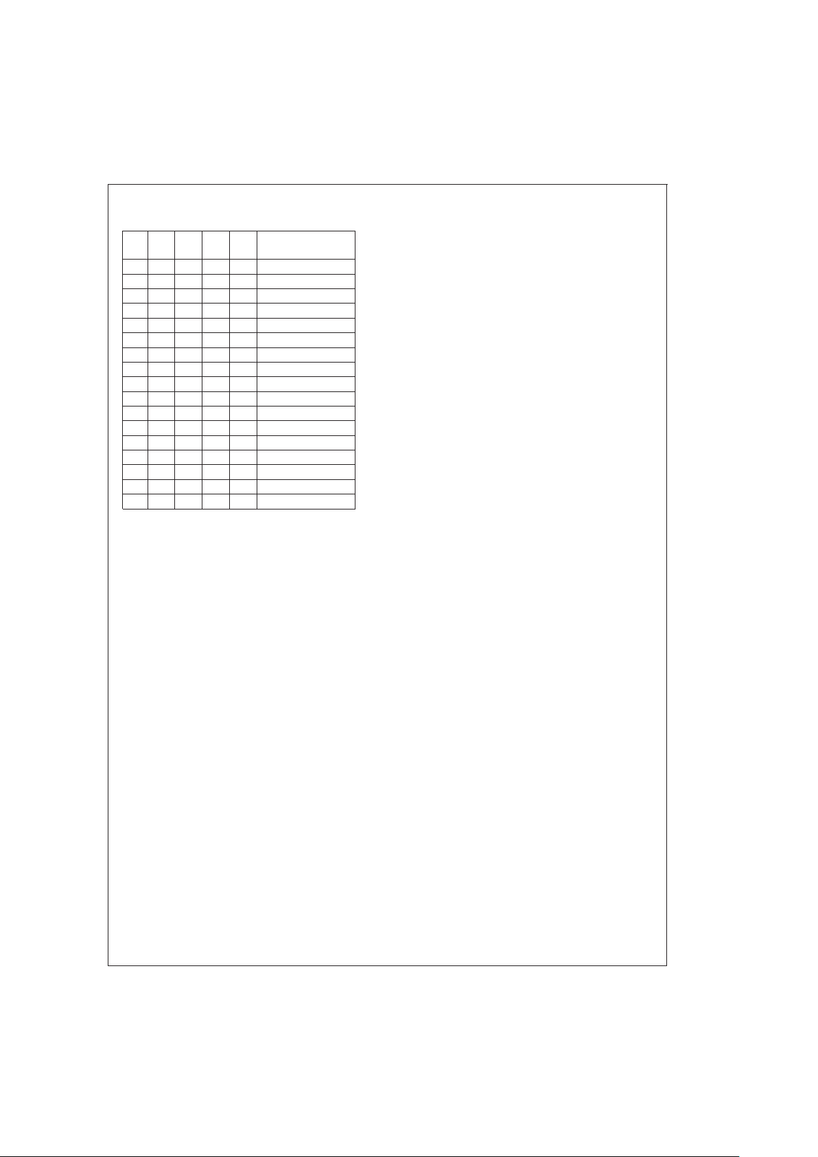
VID4:0 (Pins 14, 15, 16, 17, 18): Voltage Identification
Code. The five pins accept an open-ground pattern 5-bit binary code from outside the chip (typically from the CPU) for
generating the desired output voltage. Each VID pin is internally pulled up to V
CC
via a 90 µA current source.
Table 1
shows the code table.
OUTEN (Pin 19): Output Enable. The output voltage is dis-
abled when this pin is pulled low. It is internally pulled up to
V
CC
via a 90 µA current source.
HSGATE (Pin 20): Gate drive for the high-side N-channel
MOSFET. This signal is interlocked with LSGATE (Pin 1) to
avoid a shoot-through problem.
TABLE 1. VID Code and DAC Output
V
ID4VID3VID2VID1VID0
Rated Output
Voltage (V)
01111 1.30
01110 1.35
01101 1.40
01100 1.45
01011 1.50
01010 1.55
01001 1.60
01000 1.65
00111 1.70
00110 1.75
00101 1.80
00100 1.85
00011 1.90
00010 1.95
00001 2.00
TOP VIEW
DS100834-3
Plastic SO-20
Order Number LM2636M
See NS Package Number M20B
TOP VIEW
DS100834-3
Plastic TSSOP-20
Order Number LM2636MTC
See NS Package Number MTC20
LM2636
www.national.com 2
Page 3
Pin Descriptions (Continued)
TABLE 1. VID Code and DAC Output (Continued)
V
ID4VID3VID2VID1VID0
Rated Output
Voltage (V)
00000 2.05
11111 (shutdown)
11110 2.1
11101 2.2
11100 2.3
11011 2.4
11010 2.5
11001 2.6
11000 2.7
10111 2.8
10110 2.9
10101 3.0
10100 3.1
10011 3.2
10010 3.3
10001 3.4
10000 3.5
LM2636
www.national.com3
Page 4

Absolute Maximum Ratings (Note 1)
If Military/Aerospace specified devices are required,
please contact the National Semiconductor Sales Office/
Distributors for availability and specifications.
(All voltages are referenced to the PGND and SGND pins.)
V
CC
7V
BOOTV 18V
Junction Temperature 150˚C
DC Power Dissipation (Note 2) 1.42W
Storage Temperature −65˚C to +150˚C
Soldering Time, Temperature
Wave (4 seconds)
Infrared (10 seconds)
Vapor Phase (75 seconds)
260˚C
240˚C
219˚C
ESD Susceptibility (Note 3) 2 kV
Recommended Operating
Conditions
(Note 1)
Supply Voltage Range (V
CC
) 4.5V to 5.5V
Junction Temperature Range 0˚C to +125˚C
Electrical Characteristics
VCC= 5V unless otherwise indicated under the Conditions column. Typicals and limits appearing in plain type apply for TA=
T
J
= +25˚C. Limits appearing in boldface type apply over 0˚C to +70˚C.
Symbol Parameter Conditions Min Typ Max Units
V
BOOTV
FET Driver Supply
Voltage
18 V
V
DACOUT
5-Bit DAC Output
Voltage
VID4:0=01111 1.284 1.304 1.324
V
VID4:0=01101 1.385 1.406 1.427
VID4:0=01011 1.483 1.506 1.529
VID4:0=01001 1.585 1.609 1.633
VID4:0=00111 1.683 1.709 1.735
VID4:0=00101 1.784 1.811 1.838
VID4:0=00001 1.983 2.013 2.043
VID4:0=11101 2.173 2.206 2.239
VID4:0=11010 2.471 2.509 2.547
VID4:0=10111 2.768 2.81 2.852
∆V
OUT
DC Load Regulation I
OUT
=0 to 14A
Figure 2
−5
mV
DC Line Regulation V
IN
=4.75V to 5.25V
Figure 2
1
G
EA
Error Amplifier DC Gain 85 dB
SR
EA
Error Amplifier Slew
Rate
6 V/µs
BW
EA
Error Amplifier Unity
Gain Bandwidth
5 MHz
I
Q_V
CC
Operating VCCCurrent OUTEN=VCC=5V, VID=10111 1.5 2.5 4
mA
Shutdown V
CC
Current OUTEN Floating, VID0:4 Floating 1 1.5 3
I
Q_BOOTV
BOOTV Pin Quiescent
Current
BOOTV=12V, OUTEN=0, VID0:4
Floating
4µA
D
MAX
Maximum Duty Cycle 90
%
D
MIN
Minimum Duty Cycle 0
%
R
SENSE
SENSE Pin Resistance
to Ground
7 11.5 16 kΩ
R
DS_SRC
FET Driver
Drain-Source ON
Resistance when
Sourcing Current
BOOTV=5V
7 Ω
R
DS_SINK
FET Driver
Drain-Source ON
Resistance when
Sinking Current
(Independent of BOOTV Voltage)
1.7 Ω
f
OSC
Oscillator Frequency RFA=84kΩ 250 300 350
kHzR
FA
=22kΩ 1000
R
FA
= 10.5 kΩ 2000
I
MAX
IMAX Pin Sink Current V
IMAX
= 5V, V
IFB
= 6V, VCC=5V 130 180 230 µA
LM2636
www.national.com 4
Page 5

Electrical Characteristics (Continued)
VCC= 5V unless otherwise indicated under the Conditions column. Typicals and limits appearing in plain type apply for TA=
TJ= +25˚C. Limits appearing in boldface type apply over 0˚C to +70˚C.
Symbol Parameter Conditions Min Typ Max Units
V
OUTEN_IH
OUTEN Pin Input Logic
Low to Logic High Trip
Point
OUTEN Voltage
↑
3.5 3.0 V
V
OUTEN_IL
OUTEN Pin Input Logic
High to Logic Low Trip
Point
OUTEN Voltage
↓
1.8 1.5 V
V
REF
Band Gap Reference I
VREF
=0mA 1.225 1.256 1.287 V
V
REF_LOAD
Reference Voltage at
Full Load
I
VREF
= 0.5 mA, Sourcing
1.223 1.254 1.285 V
V
REF_525
Reference Voltage at
High Line
I
VREF
= 0 mA, VCC= 5.25V
1.226 1.257 1.288 V
V
REF_475
Reference Voltage at
Low Line
I
VREF
= 0 mA, VCC= 4.75V
1.224 1.255 1.286 V
∆V
REF_LOAD
Reference Voltage
Load Regulation
I
VREF
= 0.5 mA, Sourcing
−2 mV
∆V
REF_LINE
Reference Voltage Line
Regulation
I
VREF
= 0 mA, VCCChanges from
5.25V to 4.75V
−0.5 mV
V
SAWL
Ramp Signal Valley
Voltage
1.25 V
V
SAWH
Ramp Signal Peak
Voltage
3.25 V
V
PWRBAD_GD
PWRGD Pin↓Trip
Points (see Pin
Description for Pin 13)
%
above DAC Output Voltage, when
Output Voltage
↑
10
%
%
below DAC Output Voltage, when
Output Voltage
↓
−10
V
PWRGD_BAD
PWRGD Pin↑Trip
Points (see Pin
Description for Pin 13)
%
above DAC Output Voltage, when
Output Voltage
↓
8
%
%
below DAC Output Voltage, when
Output Voltage
↑
−8
V
OVP
Over-voltage Protection
Trip Point
%
above DAC Output Voltage
15
%
t
PWRGD
Power Good Response
Time
V
SENSE
Rises from 0V to Rated
V
OUT
2 6 15 µs
t
PWRBAD
Power Not Good
Response Time
V
SENSE
Falls from Rated V
OUT
to 0V
2 6 15 µs
I
OUTEN
OUTEN Pin Internal
Pull-Up Current
60 90 130 µA
V
VID_IH
VID Pins Logic High
Trip Point
3.5 3.0 V
V
VID_IL
VID Pins Logic Low
Trip Point
1.8 1.3 V
I
VID
VID0:4 Internal Pull-Up
Current
60 90 130 µA
t
SS
Soft Start Duration
2048
clock
cycles
Note 1: Absolute Maximum Ratings are limits beyond which damage to the device may occur.Recommended Operating Conditions are conditions under which
the device operates correctly. Recommended Operating Conditions do not imply guaranteed performance limits.
Note 2: Maximum allowable DC power dissipation is a function of the maximum junction temperature, T
JMAX
, the junction-to-ambient thermal resistance, θJA, and
the ambient temperature, T
A
. The maximum allowable power dissipation at any ambient temperature is calculated using:
The junction-to-ambient thermal resistance, θJA, for LM2636 in the M20B package is 88˚C/W, and 120˚C/W for the MTC20 package.
LM2636
www.national.com5
Page 6

Electrical Characteristics (Continued)
Note 3: All pins are rated for 2 kV, except for the I
MAX
pin (Pin 7) which is rated for 1.5 kV.
Block Diagram
Test Circuit
DS100834-2
DS100834-4
FIGURE 2.
LM2636
www.national.com 6
Page 7

Applications Information
OVERVIEW
The LM2636 is a high speed synchronous PWM buck regulator controller designed for VRM vendors or motherboard
manufacturers who need to build on-board power supplies
for Cyrix MII, Pentium II or Deschutes microprocessors. It
has a built-in 5-bit DAC to decode the 5-bit word provided by
the CPU and supply the corresponding voltage. It also has
the power good (PWRGD) and output enable (OUTEN) functions required by the VRM specification. It employs a voltage
mode control scheme plus two fast responding comparators
to quickly respond to large load transients. It has two fast
FET drivers to drive the high-side and low-side NMOS
switches of a synchronous buck regulator. The PWM frequency is adjustable from 50 kHz to 1 MHz through an external resistor. Over-voltage protection is achieved by shutting
off the high-side driver and turning on the low-side driver
100%of the time. Current limiting is implemented by sensing
V
DS
of the high-side NMOS switch and shutting it off for the
present switching cycle when an over current condition is detected. Soft start functionality is realized through an internal
digital counter and an internal DAC.
THEORY OF OPERATION
Start Up
When V
CC
voltage exceeds 4.2V,OUTEN pin is a logic high
and the VID code is valid, the soft start circuitry starts to
work. The duration of the soft start is determined by an internal digital counter and the switching frequency. During soft
start, the output of the error amplifier is allowed to increase
gradually.When the counter has counted 2,048 clock cycles,
the soft start session ends and the output voltage level of the
error amplifier is released and allowed to go to a value that is
determined by the feedback loop. PWRGD pin is forced low
during soft start and is turned over to output voltage monitoring circuitry after that. Before V
CC
reaches 4.2V, all internal
logic is in a power on reset state and the two FET drivers are
disabled.
During normal operation, if V
CC
voltage drops below 3.8V,
the internal circuitry will go into power on reset again. The
hysteresis helps decrease the noise sensitivity on the V
CC
pin. After soft starts ends and during normal operation, if the
converter output voltage exceeds 115%of the DAC output
voltage, the LM2636 will lock into over voltage protection
mode. The high side drive will be disabled, and the low side
drive will be high. There are two ways to clear the mode. One
is to cycle V
CC
voltage once. The other is to toggle the
OUTEN level. After the over voltage protection mode is
cleared, the LM2636 will enter the soft start session and start
over.
Normal Operation
During the normal operation mode, the LM2636 regulates
the converter output voltage by adjusting the duty ratio. The
output voltage is determined by the 5-bit VID code set by the
user/load.
The PWM frequency is set by the external resistor between
FREQ_ADJ pin and ground. The resistance needed for a desired switching frequency is:
For example, if the desired switching frequency is 300 kHz,
the resistance should be around 84 kΩ.
The minimum allowable PWM frequency is 5 kHz.
MOSFET Gate Drive
The LM2636 has two gate drives that are suitable for driving
external N-MOSFETs in a synchronous buck topology. The
power for the two FET drivers is supplied by the BOOTV pin.
This BOOTV voltage needs to be at least one V
GS(th)
higher
than the converter input voltage for the high side FET to be
fully turned on. The voltage can be either supplied from
a separate source other than the input voltage or can be
generated locally by utilizing a charge pump structure. In a
typical desktop microprocessor application, if 5V is chosen
to be the input voltage, then 12V can be used for the
BOOTV. If 12V is not available, a simple charge pump circuitry consisting of a diode and a small capacitor can be
used, as shown in
Figure 3
.
When the low side FET is on, the charge pump capacitor is
charged to near the input voltage through the diode. When
low side FET is turned off, the high side FET driver is enabled, and the charge pump capacitor starts to charge the
high side FET gate until it is fully on. By this time the high
side FET source node will fly to close to input voltage level
and the upper node of the capacitor will also fly to one input
voltage higher than the input voltage, enabling the high side
FET driver to continue working.
For a BOOTV of 12V, the initial gate charging current is typically 2A, and the initial gate discharging current is typically
6A, good for high speed switching.
The LM2636 gate drives are of BiCMOS design. Unlike
some other bipolar VRM control ICs, the gate drive has railto-rail swing that ensures no spurious turn-on due to capacitive coupling.
Another feature of the FET gate drives is the adaptive nonoverlapping mechanism. A gate driver is not turned on until
the other is fully off. The dead time in between is typically 20
ns. This avoids the potential shoot-through problem and
helps improve efficiency.
Load Transient Response
In a typical modern MPU application such as the Pentium II
core voltage power supply, load transient response is a critical issue. The LM2636 utilizes the conventional voltage
feedback technology as the primary feedback control
method. When the load transient happens, the error in the
output voltage level is fed to the error amplifier. The output of
DS100834-6
FIGURE 3. BOOTV Voltage Supplied by a Charge Pump
LM2636
www.national.com7
Page 8

Applications Information (Continued)
the error amplifier is then compared with an
internally generated PWM ramp signal and the result of the
comparison is a series of pulses with certain duty ratios.
These pulses are used to control the turn-on and turn-off of
the MOSFET gate drivers. In this way, the error in the output
voltage gets “compensated” or cancelled by the change in
the duty ratio of the FET switches. During a large load transient, depending on the compensation design, the change in
duty ratio can be as fast as less than one switching cycle.
Refer to Design Considerations section for more details.
Besides the usual voltage mode feedback control loop, the
LM2636 also has a pair of fast comparators (the MIN and
MAX comparators) to help maintain the output voltage during a large and fast load transient. The trip points of the comparators are set to
±
5%of the DAC output voltage. When
the load transient is so large that the output voltage goes
outside the
±
5%window, the MIN or MAX comparator will
bypass the primary voltage control loop and immediately set
the duty ratio to either maximum value or to zero. This provides the fastest possible way to react to such a large load
transient in a classical buck converter.
Power Good Signal
The power good signal is used to indicate that the output
voltage is within specified range. In the LM2636, the range is
set to a
±
10%window of the DAC output voltage. During soft
start, the power good signal is always low.At the end of the
soft start session,the output voltage is checked and the
PWRGD pin will be asserted if the voltage is within specified
range.
Over Voltage Protection
When the output voltage exceeds 115%of the DAC output
voltage after the end of soft start, the LM2636 will enter over
voltage protection mode in which it shuts itself down. The upper gate driver is held low while the lower gate driver is held
high. PWRGD will be low. For LM2636 to recover from OVP
mode, either OUTEN or V
CC
voltage has to be toggled. Another more subtle way to recover is to float all the VID pins
and reapply the correct code.
Current Limit
Current limit is realized by sensing the V
DS
voltage of the
high side MOSFET when it is on. Since the r
DS_ON
of a
MOSFET is a known value, current through the MOSFET
can be known by monitoring V
DS
. The relationship between
the three parameters is:
To implement the current limit function, an external resistor
R
IMAX
is need. The resistor should be connected between
the drain of the high side MOSFET and the IMAX pin. A constant current of around 180 µA is forced into the IMAX pin
and causes a fixed voltage drop across the R
IMAX
resistor.
This voltage drop is then compared with the V
DS
of the high
side MOSFET and if the latter is higher, over current is
reached. So the appropriate value of R
IMAX
for a predetermined current limit level I
LIM
can be calculated by the
following equation:
For example, if we know that the r
DS_ON
of the MOSFET is
20 mΩ, and the current limit we want to set is 20A, then we
should choose the value of R
IMAX
to be 2.2 kΩ.
To provide the greatest protection over the high side MOSFET, cycle by cycle protection is implemented. The sampling
of the V
DS
starts as early as about 300 ns after the switch is
turned on. Whenever an over current condition is detected,
the high side switch is immediately turned off and the low
side switch turned on, until the next switching cycle comes.
The delay of 300 ns is to circumvent switching noise when
the MOSFET is first turned on.
DESIGN CONSIDERATIONS
Control Loop Compensation
A switching regulator should be properly compensated to
achieve a stable condition. For a synchronous buck regulator that needs to meet stringent load transient requirement
such as a Pentium II MPU core voltage supply, a simple
2-pole-1-zero compensation network should suffice, such as
the one shown in
Figure 4
(C1,C2,R1and R2). This is because the ESR zero of the typical output capacitors is low
enough to make the control-to-output transfer function a
single-pole-roll-off.
As an example, let us figure out the values of the compensation network components in
Figure 4
. Assume the following
parameters:R=20Ω,R
L
=20mΩ,RC=9mΩ,L=2µH,
C = 7.5 mF, V
IN
=5V,Vm= 2V and switching frequency
= 300 kHz. These parameters are based on the typical application in
Figure 1
. Notice RLis the sum of the inductor DC re-
sistance and the on resistance of the MOSFETs.
DS100834-9
FIGURE 4. Buck Converter from a Control Point of
View
LM2636
www.national.com 8
Page 9

Applications Information (Continued)
The control-to-output transfer function is
The ESR zero frequency is:
The power stage double pole frequency is:
The corresponding Bode plots are shown in
Figure 5
.
Since the ESR zero frequency is so low,it effectively cancels
the phase shift from one of the power stage poles. This limits
the total phase shift to 90%.
Although this regulator design is stable (phase shift is
<
90˚
when gain=0dB), it needs compensation to improve the DC
gain and cut off frequency (0dB frequency). Otherwise, the
low DC gain may cause a poor line regulation, and the low
cutoff frequency will hurt transient response performance.
The transfer function for the 2-pole-1-zero compensation
network shown in
Figure 4
is:
where
One of the poles is located at origin to help achieve the highest DC gain. So there are three parameters to determine, the
position of the zero, the position of the second pole, and the
constant A. To determine the cutoff frequency and phase
margin, the loop bode plots need to be generated. The loop
transfer function is:
TF = −TF1 x TF2
By choosing the zero close to the double pole position and
the second pole to half of the switching frequency,the closed
loop transfer function turns out to be very good.
That is, if f
Z
= 1.32 kHz, fP= 153 kHz, and A = 4.8 x 10⁻⁶ΩF,
then the cutoff frequency will be 50 kHz, the phase margin
will be 72˚, and the DC gain will be that of the error amplifier.
See
Figure 6
below.
The compensation network component values can be determined by the following equations:
Notice there are three equations but four variables. So one
of the variables can be chosen arbitrarily. Since the current
driving capability of the error amplifier is limited to around
3 mA, it is a good idea to have a high impedance path from
the output of the error amplifier to the output of the converter.
From the above equations it can be told that a larger R
2
will
DS100834-13
FIGURE 5. Control-to-Output Bode Plots
DS100834-17
FIGURE 6. Loop Bode Plots
LM2636
www.national.com9
Page 10

Applications Information (Continued)
result in a smaller C
1,C2
and a larger R1. However, too large
an R
1
can also bring error due to the bias current required by
the inverting input pin of the error amplifier. Calculations
show that the following combination is a good one: R
2
=51Ω,
C
1
= 0.022 µF, R1= 5.6 kΩ,C2= 820 pF.
For a different application or different type of output capacitors, a different compensation scheme may be necessary.
The user can either follow the steps above to figure the appropriate component values or contact the factory for help.
MOSFET SELECTION
The selection of MOSFET switches affects both the efficiency of the whole converter and the current limit setting.
From an efficiency point of view it is suggested that for the
high-side switch, only logic level MOSFETs be used. Standard MOSFETs can be used for the low side switch when
12V is used to power the BOOTV pin. The lower loss associated with the MOSFETs is two-fold—Ohmic loss and
switching loss. The Ohmic loss is easy to calculate whereas
the switching loss is much more difficult to estimate. In general the switching loss is directly proportional to the switching
frequency. As the power MOSFET technology advances,
lower and lower gate charge devices will be available. That
should allow the user to go to higher switching frequencies
without the penalty of losing too much efficiency.
As an example, let us select the MOSFETs for a converter
with a target efficiency of 80%at a load of 2.8V, 14A. Assume the inductors lose 1W, the capacitors lose 0.75W and
the total switching loss at 300 kHz is 3.2W. The total allowed
power loss is 9.8W, so the MOSFET Ohmic loss should not
exceed 4.9W. Assume the two switches have the same conduction loss, i.e., 2.5W each, then the ON resistance for the
two switches is:
The low side switch ON resistance is much higher than the
high side because at 2.8V the duty cycle is higher than 50
%
and becomes even larger at full load. For the high side
switch, an IRL3202 (TO-220 package) or IRL3202S (D
2
PAK)
should be sufficient. For the low side switch, an IRL3303
(TO-220 package) or IRL3303S (D
2
PAK) should be sufficient. Since each FET is dissipating 3.2W/2 + 2.5W = 4.1W,
it is suggested that appropriate heat sinks be used in the
case of TO-220 package or large enough copper area be
connected to the drain in the case of surface mount package.
CAPACITOR SELECTION
The selection of capacitors is an extremely important step
when designing a converter for a load such as the
Pentium II. Since the typical slew rate of the load current during a large load transient is around 20A/µs to 30A/µs, the
switching converter has to rely on the output capacitors to
take care of the first few microseconds. Under such a current
slew rate, ESR of the output capacitors is more of a concern
than the ESL. Depending on the kind of capacitors being
used, capacitance of the output capacitors may or may not
be an important factor. When the output capacitance is too
low, the converter may have to have a small output inductor
to quickly supply current to the output capacitors when the
load suddenly kicks in and to quickly stop supplying current
when the load is suddenly removed.
Multilayer ceramic (MLC) capacitors can have very low ESR
but also a low capacitance value compared to other kinds of
capacitors. Low ESR aluminum electrolytic capacitors tend
to have large sizes and capacitances. Tantalum electrolytic
capacitors can have a fairly low ESR with a much smaller
size and capacitance than the aluminum capacitors. Certain
OSCON capacitors present ultra low ESR and long life span.
By the time the total ESR of the output capacitor bank
reaches around 9 mΩ, the capacitance of the aluminum/
tantalum/OSCON capacitors is usually already in the millifarad range. For those capacitors, ESR is the only factor to
consider.MLCs can have the same amount of total ESR with
much less capacitance, most probably under 100 µF.A very
small inductor, ultra fast control loop and a high switching
frequency become necessary in such a case to deal with the
fast charging/discharging rate of the output capacitor bank.
From a cost savings point of view, aluminum electrolytic capacitors are the most popular choice for output capacitors.
They have reasonably long life span and they tend to have
huge capacitance to withstand the charging or discharging
process during a load transient for a fairly long period. Sanyo
MV-GX series gives good performance when enough of the
capacitors are paralleled. The 6MV1500GX capacitor has a
typical ESR of 44 mΩ. Five of these capacitors should be
sufficient in the case of on-board power supply for a Pentium
II motherboard.
The challenge for input capacitors is the ripple current. The
large ripple current drawn by the high side switch tends to
generate quite some heat due to the capacitor ESR. The
ripple current ratings in the capacitor catalogs are usually
specified under the highest allowable temperature. In the
case of desktop applications, those ratings seem too conservative.Agood way to ensure enough number of capacitors is
through lab evaluation. The input current RMS ripple value
can be determined by the following equation:
and the power loss in each input capacitor is:
In the case of Pentium II power supply, the maximum output
current is around 14A. Under the worst case when duty cycle
is 50%, the maximum input capacitor RMS ripple current is
half of output current, i.e., 7A. It is found that three Sanyo
16MV820GX capacitors are enough under room temperature. The typical ESR of those capacitors is 44 mΩ.Sothe
power loss in each of them is around (7A)
2
x44mΩ/32=
0.24W. Note that the power loss in each capacitor is inversely proportional to the square of the total number of capacitors, which means the power loss in each capacitor
quickly drops when the number of capacitors increases.
INDUCTOR SELECTION
The size of the output is determined by a number of parameters. Basically the larger the inductor, the smaller the output
ripple voltage, but the slower the converter’s response
speed during a load transient. On the other hand, a smaller
inductor requires higher switching frequency to maintain the
same level of output ripple, and probably results in a more
lossy converter, but has less inertia responding to load tran-
LM2636
www.national.com 10
Page 11

Applications Information (Continued)
sient. In the case of Pentium II power supply, fast recovery of
the load voltage from transient window back to the steady
state window is considered important. This limits the highest
inductance value that can be used. The lowest inductance
value is limited by the highest switching frequency that can
be practically employed. As the switching frequency increases, the switching loss in the MOSFETs tends to increase, resulting in less converter efficiency and larger heat
sinks. A good switching frequency is probably a frequency
under which the MOSFET conduction loss is higher than the
switching loss because the cost of the MOSFET is directly
related to its R
DSON
. The inductor size can be determined by
the following equation:
where V
O_RIP
is the peak-to-peak output ripple voltage, f is
the switching frequency. For commonly used low R
DSON
MOSFETs, a reasonable switching frequency is 300 kHz. Assume an output peak-peak ripple voltage of 18 mV is to be
guaranteed, the total output capacitor ESR is 9 mΩ, the input
voltage is 5V, and output voltage is 2.8V. The inductance
value according to the above equation will then be 2 µH. The
highest slew rate of the inductor current when the load
changes from no load to full load can be determined as follows:
where D
MAX
is the maximum allowed duty cycle, which is
around 0.9 for LM2636. For a load transient from 0A to 14A,
the highest current slew rate of the inductor, according to the
above equation, is 0.85A/µs, and therefore the shortest possible total recovery time is 14A/(0.85A/µs) = 16.5 µs. Notice
that the output voltage starts to recover whenever the inductor starts to supply current.
The highest slew rate of the inductor current when the load
changes from full load to no load can be determined from the
same equation, but use D
MIN
instead of D
MAX
.
Since the D
MIN
of LM2636 at 300 kHz is 0%, the slew rate is
therefore −1.4A/µs. So the approximate total recovery time
will be 14A/(1.4A/µs) = 10 µs.
The input inductor is for limiting the input current slew rate
during a load transient. In the case that low ESR aluminum
electrolytic capacitors are used for the input capacitor bank,
voltage change due to capacitor charging/discharging is usually negligible for the first 20 µs. ESR is by far the dominant
factor in determining the amount of capacitor voltage
undershoot/overshoot due to load transient. So the worst
case is when the load changes between no load and full
load, under which condition the input inductor sees the highest voltage change across the input capacitors. Assume the
input capacitor bank is made up of three 16MV820GX, i.e.,
the total ESR is 15 mΩ. Whenever there is a sudden load
current change, it has to initially be supported by the input
capacitor bank instead of the input inductor.So for a full load
swing between 0A and 14A, the voltage seen by the input inductor is ∆V=14Ax15mΩ= 210 mV. Use the following
equation to determine the minimum inductance value:
where (di/dt)
MAX
is the maximum allowable input current
slew rate, which is 0.1A/µs in the case of the Pentium II
power supply. So the input inductor size, according to the
above equation, should be 2.1 µH.
DYNAMIC POSITIONING OF LOAD VOLTAGE
Since the Intel VRM specifications have defined two operating windows for the MPU core voltage, one being the steady
state window and the other the transient window, it is a good
idea to dynamically position the steady state output voltage
in the steady state window with respect to load current level
so that the output voltage has more headroom for load transient response. This requires information about the load current. There are at least two simple ways to implement this
idea with LM2636. One is to utilize the output inductor DC resistance, see
Figure 7
. The average voltage across the output inductor is actually that across its DC resistance. That
average voltage is proportional to load current.
Since the switching node voltage V
A
bounces between the
input voltage and ground at the switching frequency, it is impossible to choose point A as the feedback point, otherwise
the dynamic performance will suffer and the system may
have some noise problems. Using a low pass filter network
around the inductor, such as the one shown in the figure,
seems to be a good idea. The feedback point is C.
Since at the switching frequency the impedance of the 0.1
µF is much less than 5 kΩ, the bouncing voltage at point A
will be mainly applied across the resistor 5 kΩ, and point C
will be much quieter thanA. However, V
CB
average is still the
majority of V
AB
average, because of the resistor divider. So
in steady state V
C=IOxrL+VCORE
, where rLis the inductor
DC resistance. So at no load, output voltage is equal to V
C
,
and at full load, output voltage is I
OxrL
lower than VC. Tofurther utilize the steady state window, a resistor can be connected between the FB pin and ground to increase the no
load output voltage to close to the upper limit of the window.
DS100834-26
FIGURE 7. Dynamic Voltage Positioning by Utilizing
Output Inductor DC Resistance
LM2636
www.national.com11
Page 12

Applications Information (Continued)
A possible drawback of the scheme in
Figure 7
is slow transient recovery speed. Since the 5 kΩresistor and the 0.1 µF
capacitor have a large time constant, the settling of point C
to its steady state value during a load transient may take a
few milliseconds. Depending on the interaction between the
compensation network and the 0.1 µF capacitor, V
core
may
take different routes to reach its steady state value. This is
undesired when the load transients happens more than 1000
times per second. Reducing the time constant will result in a
more fluctuating V
C
due to a less effective low pass filter.
Fine tuning the parameters may balance the tradeoffs.
Another way to implement the dynamic voltage positioning is
through the use of a stand-alone resistor, such as the 4 mΩ
resistor in
Figure 8
above. The advantage of this implemen-
tation over the previous one is a much faster speed of V
CORE
from transient level to steady state level. The disadvantage
is less efficiency. The total power loss can be 0.78W at 14A
of load current. The cost of the resistor can be minimized by
implementing it through a PCB trace.
REFERENCE VOLTAGE
The V
REF
pin can have many uses, such as in the watchdog
circuitry and in an LDO controller.
Figure 9
shows an applica-
tion where V
REF
is used to build a N-FET LDO controller.An
appropriate compensation network is necessary to tailor the
dynamic performance of the whole power supply.
PCB LAYOUT CONSIDERATIONS
There are several points to consider.
1. Try to use 2 oz. copper for the ground plane if tight load
regulation is desired. In the case of dynamic voltage positioning, this may not be a concern because the loose
load regulation is desired anyway. However, do not forget to take into consideration the voltage drop caused by
the ground plane when calculating dynamic voltage positioning parameters.
2. Try to keep gate traces short. However, do not make
them too short or else the LM2636 may stay too close to
the MOSFETs and get heated up by them. For the same
reason, do not use wide traces, 10 mil traces should be
enough.
3. When not employing dynamic voltage positioning, place
the feedback point at the VRM connector pins to have a
tight load regulation. If it is an on-board power supply,
place the feedback point at Slot I connector or wherever
is closest to the MPU.
4. Start component placement with the power devices such
as MOSFETs and inductors.
5. Do not place the LM2636 directly underneath the MOS-
FETs when when surface mount MOSFETs are used.
6. If possible, keep the capacitors some distance away
from the inductors so that the capacitors will have a
lower temperature environment.
7. When implementing dynamic voltage positioning
through a PCB trace, be aware that the PCB trace is a
heat source and try to avoid placing the trace directly underneath the LM2636.
DS100834-27
FIGURE 8. Dynamic Voltage Positioning by Using A
Stand-Alone Resistor
DS100834-28
FIGURE 9. V
REF
Used in an N-FET LDO Supply
LM2636
www.national.com 12
Page 13

Physical Dimensions inches (millimeters) unless otherwise noted
20-Lead Plastic SO Package
Order Number LM2636M
NS Package Number M20B
LM2636
www.national.com13
Page 14

Physical Dimensions inches (millimeters) unless otherwise noted (Continued)
LIFE SUPPORT POLICY
NATIONAL’S PRODUCTS ARE NOT AUTHORIZED FOR USE AS CRITICAL COMPONENTS IN LIFE SUPPORT
DEVICES OR SYSTEMS WITHOUT THE EXPRESS WRITTEN APPROVAL OF THE PRESIDENT AND GENERAL
COUNSEL OF NATIONAL SEMICONDUCTOR CORPORATION. As used herein:
1. Life support devices or systems are devices or
systems which, (a) are intended for surgical implant
into the body, or (b) support or sustain life, and
whose failure to perform when properly used in
accordance with instructions for use provided in the
labeling, can be reasonably expected to result in a
significant injury to the user.
2. A critical component is any component of a life
support device or system whose failure to perform
can be reasonably expected to cause the failure of
the life support device or system, or to affect its
safety or effectiveness.
National Semiconductor
Corporation
Americas
Tel: 1-800-272-9959
Fax: 1-800-737-7018
Email: support@nsc.com
National Semiconductor
Europe
Fax: +49 (0) 1 80-530 85 86
Email: europe.support@nsc.com
Deutsch Tel: +49 (0) 1 80-530 85 85
English Tel: +49 (0) 1 80-532 78 32
Français Tel: +49 (0) 1 80-532 93 58
Italiano Tel: +49 (0) 1 80-534 16 80
National Semiconductor
Asia Pacific Customer
Response Group
Tel: 65-2544466
Fax: 65-2504466
Email: sea.support@nsc.com
National Semiconductor
Japan Ltd.
Tel: 81-3-5639-7560
Fax: 81-3-5639-7507
www.national.com
20-Lead Plastic TSSOP (MTC)
Order Number LM2636MTC
NS Package Number MTC20
LM2636 5-Bit Programmable Synchronous Buck Regulator Controller
National does not assume any responsibility for use of any circuitry described, no circuit patent licenses are implied and National reserves the right at any time without notice to change said circuitry and specifications.
 Loading...