

Page 1
LM2630
Synchronous Step-Down Power Supply Controller
General Description
The LM2630 controller provides all the active functions for
step-down (buck)switching converters. These dc-to-dc converters provide core CPU power in battery-operated systems.
High efficiency is achieved by using synchronous rectification and pulse-skipping mode operation at light load. Inexpensive N-channel MOSFETs are used to reduce system
cost. Bootstrap circuit is used to drive the high-side
N-channel MOSFET.
Current mode control schemeis used to improve line regulation and transient response, also provides cycle-by-cycle
current limiting.
The operating frequency is adjustable between 200 kHz and
400 kHz. An external shutdown pin can be used to disable
the device and reducethe quiescent current to 0.1µA. In low
noise applications, bringing theFPWMpin high can force the
device to operate in constant frequency mode. Other features include the external synchronization pin, and the
PGOOD pin to indicate the state of the output voltage.
Protection circuitry includesthermal shutdown, undervoltage
shut down, soft-startcapability,and two levelsof current limits: The first levelsimply limits the load currentdirectly; at the
second level, if the load pulls the output voltage down below
80%of the regulated value, the chip willshut down. This
latched operation is disabled during startup, but an internal
timer will enable it if the outputdoes not come up in the preset time.
Features
n 4.5V to 30V input range
n Adjustable output (1.8V to 6V)
n 200 kHz to 400 kHz adjustable operating frequency
n Externally synchronizable
n On-board power good function
n Precision 1.24V reference output
n 0.8 mA typical quiescent current
n 0.1 µA shutdown current
n Thermal shutdown
n Direct current limit protection
n Input undervoltage lockout
n Output Undervoltage shutdown protection
n Programmable soft-start function
n Tiny TSSOP package
Applications
n Notebook and subnotebook computers
n Cellular phones
n Portable instruments
n Battery-powered digital devices
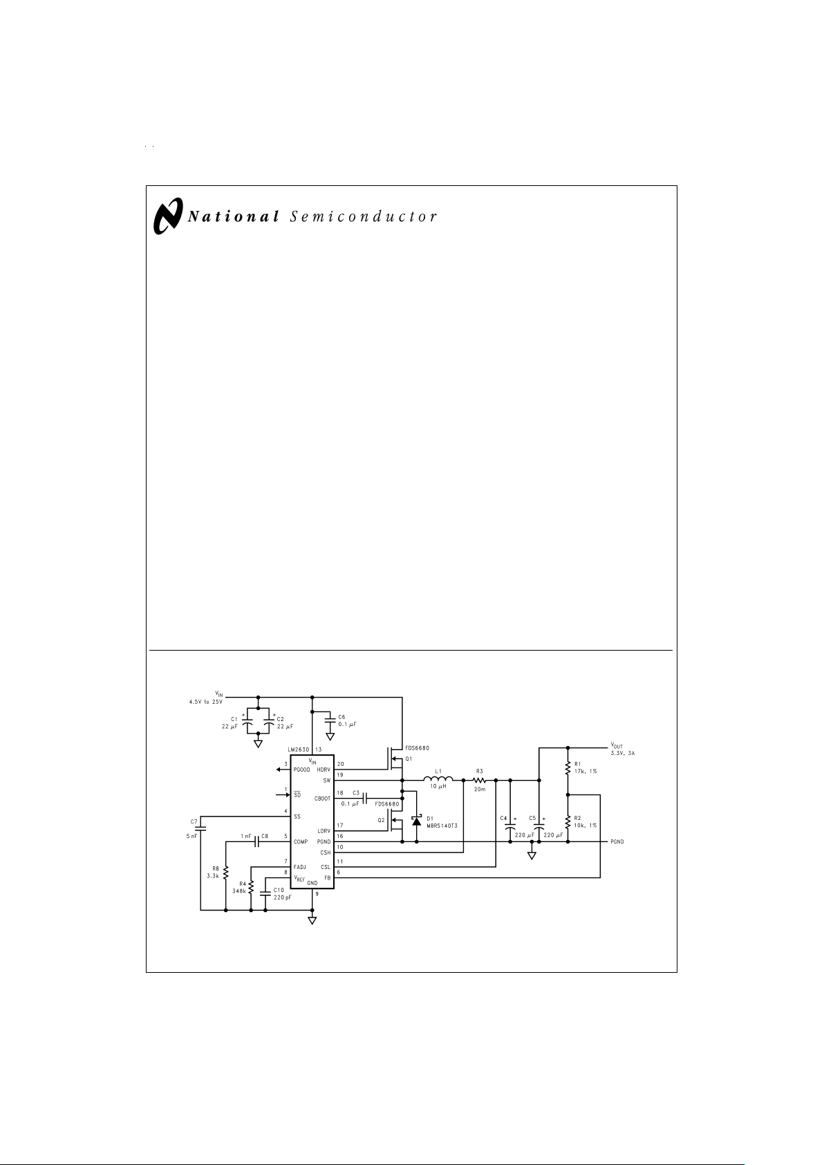
Typical Application Circuit
DS100120-1
February 1999
LM2630 Synchronous Step-Down Power Supply Controller
© 1999 National Semiconductor Corporation DS100120 www.national.com
Page 2
Absolute Maximum Ratings (Note 1)
If Military/Aerospace specified devices are required,
please contact the NationalSemiconductorSales Office/
Distributors for availability and specifications.
Voltages from the indicated
pins to GND and PGND:
V
IN
−0.3V to 31V
CBOOT −0.3V to 36V
SD
−0.3V to 31V
SW −0.3V to 31V
CSH, CSL −0.3V to 7V
FPWM, SYNC −0.3V to 10V
Power Dissipation (T
A
=
70˚C), (Note 2)
720mW
Storage Temperature Range −65˚C to +150˚C
Soldering Dwell Time,
Temperature (Note 3)
Wave 4 sec, 260˚C
Infrared 10 sec, 240˚C
Vapor Phase 75 sec, 219˚C
ESD Rating (Note 4) 1.5 kV
Operating Ratings
V
IN
4.5V to 30V
Junction Temperature −40˚C to +125˚C
Electrical Characteristics
Specifications in standard type face are for T
j
=
25˚C and those with boldface type apply over full operating junction tem-
perature range. V
IN
=
10V, GND=PGND=0V,unless otherwise stated. (Notes 5, 6)
Symbol Parameter Conditions Typical Limit Units
System
V
IN
Input Supply Voltage 4.5
30
V(min)
V(max)
V
OUT
Output Voltage Adjustment
Range
1.8
6.0
V(min)
V(max)
∆V
OUT
/
V
OUT
Load Regulation 0 mV ≤ (CSH-CSL) ≤ 75 mV
0.3
%
∆V
OUT
/
V
OUT
Line Regulation 4.5 ≤ VIN≤ 30V
0.002
%
/V
I
IN
Input Supply Current with the
Switching Controller ON
V
FB
=
1V, V
CSH
=
2.15V, V
CSL
=
2.1V
0.8 mA
1.2/1.4 mA(max)
Input Supply Current with the
Switching Controller ON
(Internal Rail is Supplied
from CSL Pin)
V
FB
=
1V, V
CSH
=
5.15V, V
CSL
=
5V
0.15 mA
Input Supply Current with the
IC Shut Down
V
SD
=
0V, V
IN
=
30V
0.1 µA
3 (Note 7) µA(max)
Minimum Output Voltage for
CSL Providing the Internal
Rail
3V
I
SS
Soft Start Source Current V
SS
=
1.5V 10 µA
5 µA(min)
13 µA(max)
Soft Start Sink Current V
SS
=
1.5V 20 µA
V
CL
Current Limit Voltage
(Voltage from CSH to CSL)
V
FB
=
1V, V
CSL
=
1.8V 110 mV
90/80 mV(min)
130/140 mV(max)
V
IN
Undervoltage Shutdown
Latch Threshold
Rising Edge 3.5 V
2.8 V(min)
V
OUT
Undervoltage
Shutdown Latch Threshold
80
%
V
OUT
65
%
V
OUT
(min)
V
OUT
Low Regulation
Comparator Enable
Threshold
97
%
V
OUT
www.national.com 2
Page 3
Electrical Characteristics (Continued)
Specifications in standard type face are for T
j
=
25˚C and those with boldface type apply over full operating junction tem-
perature range. V
IN
=
10V, GND=PGND=0V,unless otherwise stated. (Notes 5, 6)
Symbol Parameter Conditions Typical Limit Units
System
Hysteresis of Low Regulation
Comparator
2
%
V
OUT
Regulator Window Detector
Thresholds (PGOOD from
High to Low)
91 or 109
%
V
OUT
Regulator Window Detector
Thresholds (PGOOD from
Low to High)
97 or 103
%
V
OUT
Gate Drive
V
BOOT
Bootstrap Voltage (Voltage
from CBOOT to SW)
CBOOT Sourcing 100 µA 4.5 V
4.0 V(min)
I
BOOT
CBOOT Leakage Current V
CBOOT
=
7V 100 nA
High Drive Source Current V
HDRV
=
0V, V
CBOOT
=
5V 0.3 A
High Drive Sink Current HDRV Forced to 5V 0.45 A
Low Drive Source Current LDRV Forced to 0V 0.35 A
Low Drive Sink Current LDRV Forced to 5V 0.55 A
High-Side FET
On-Resistance HDRV or
LDRV
8 Ω
Low-Side FET
On-Resistance HDRV or
LDRV
4 Ω
Oscillator
F
OSC
Oscillator Frequency FADJ Open 200 kHz
172/162 kHz(min)
228/230 kHz(max)
Oscillator Frequency FADJ Sourcing 2.94 µA (Note 8) 300 kHz
255 kHz(min)
345 kHz(max)
V
FADJ
Voltage at FADJ pin 1.03 V
D
MAX
Maximum Duty Cycle FADJ Open 96
%
92
%
(min)
Maximum Frequency of
Synchronization
Low-Going 200 ns Wide
Rectangular Pulses Applied at
400 kHz at the SYNC Input
400 kHz(min)
Minimum Pulse Width of the
SYNC Signal
SYNC Pulses are Low-Going
200 ns(min)
Error Amplifier
I
FB
Feedback Input Bias Current V
FB
=
1.3V, V
CSH
=
5.15V, V
CSL
=
5V
100 nA
I
COMP
COMP Output Source
Current
V
COMP
=
0.2V, V
FB
=
1V
50 µA
COMP Output Sink Current V
COMP
=
1.2V, V
FB
=
1.4V 50 µA
Voltage Reference
V
REF
Reference Voltage
(Nominal))
I
REF
=
0µA 1.238 V
1.213/1.208 V(min)
1.263/1.268 V(max)
www.national.com3
Page 4
Electrical Characteristics (Continued)
Specifications in standard type face are for T
j
=
25˚C and those with boldface type apply over full operating junction tem-
perature range. V
IN
=
10V, GND=PGND=0V,unless otherwise stated. (Notes 5, 6)
Symbol Parameter Conditions Typical Limit Units
Voltage Reference
V
REF
Reference Voltage (Line
Regulation)
4.5V<V
IN
<
30V 1.238 V
1.213/1.208 V(min)
1.263/1.268 V(max)
Reference Voltage (Load
Regulation)
0µA
<
I
REF
<
50 µA 1.238 V
1.213/1.208 V(min)
1.263/1.268 V(max)
Logic Inputs and Outputs
V
IH
Minimum High Level Input
Voltage (SD, FPWM and
SYNC)
2.4 V(min)
V
IL
Maximum Low Level Input
Voltage (FPWM and SYNC)
0.8 V(max)
Maximum Low Level Input
Voltage (SD)
0.5
V(max)
Maximum Input Leakage
Curren1t (SD , FPWM and
SYNC)
Logic Input Voltage 0V or 5V
±
0.1 µA
V
OH
PGOOD High Level Output
Voltage
PGOOD Sourcing 50 µA 2.7 V
2.4 V(min)
V
OL
PGOOD Low Level Output
Voltage
PGOOD Sinking 50 µA 0 V
0.5 V(max)
Note 1: Absolute maximum ratings indicate limits beyond which damage to the device may occur. Electrical specifications do not apply when operating the device
outside of its rated operating conditions.
Note 2: The maximum allowable power dissipation is calculated by using P
Dmax
=
(T
Jmax-TA
)/θJA, where T
Jmax
is the maximum junction temperature, TAis the
ambient temperature, and θ
JA
is the junction-to-ambient thermal resistance of the specified package. The 720 mW rating results from using 160˚C, 70˚C, and
125˚C/W for T
Jmax,TA
, and θJArespectively.AθJAof 125˚C/W represents the worst-casecondition of no heat sinking of the 20-pinTSSOP. Heat sinking allows the
safe dissipation of more power. TheAbsoluteMaximumpowerdissipationmustbederatedby8 mW per ˚C above 70˚C ambient. The LM2630 actively limits its junction temperature to about 160˚C.
Note 3: For detailed information on soldering plastic small-outline packages, refer to the Packaging Databook available from National Semiconductor Corporation.
Note 4: For testing purposes, ESD was applied using the human-body model, a 100 pF capacitor discharged through a 1.5 kΩ resistor.
Note 5: A typical is the center of characterization data taken withT
A
=
T
J
=
25˚C. Typicals are not guaranteed.
Note 6: All limits are guaranteed. All electricalcharacteristicshavingroom-temperaturelimitsaretestedduringproduction with T
A
=
T
J
=
25˚C.All hot and cold limits
are guaranteed by correlating the electrical characteristics to process and temperature variations and applying statistical process control.
Note 7: This limit is guaranteed by design.
Note 8: Pulling 2.94 µA out of FADJ pin simulates adjusting the oscillator frequency with a 350 kΩ resistor connected from FADJ to GND.
www.national.com 4
Page 5
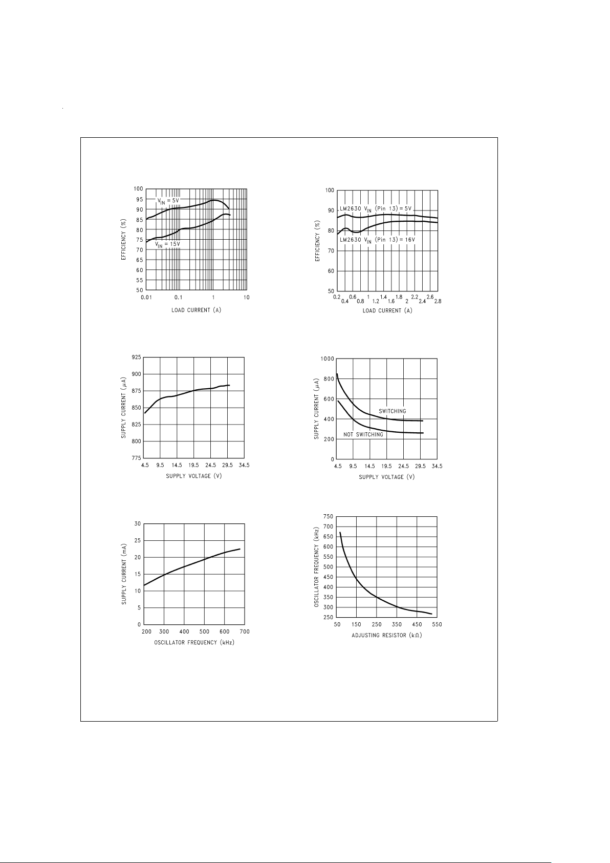
Typical Performance Characteristics
Efficiency vs Load Current
(FPWM=Low, V
OUT
=
3.3V)
DS100120-11
Efficiency (FPWM=High, Input Voltage=16V,
V
OUT
=
2.9V)
DS100120-12
Quiscent Supply Current vs Supply Voltage
(Not Switching, FPWM=Low, V
OUT
=
2.0V)
DS100120-15
Quiscent Supply Current vs Supply Voltage
(FPWM=Low, V
OUT
=
3.3V)
DS100120-16
Supply Current vs Oscillator Frequency
(FPWM=High)
DS100120-17
Oscillator Frequency vs Adjusting Resistor
DS100120-18
www.national.com5
Page 6

Typical Performance Characteristics (Continued)
Connection Diagram and Ordering Information
Pin Description
Pin Name Function
1SD
Shutdown control input, active low.
2 SYNC Oscillator synchronization input. Connect this pin to ground if not used.
3 PGOOD A constant monitor on the output voltage. PGOOD will go low if the output voltage
exceeds
±
9%of its nominal value. Once PGOOD goes low, it will go high if the output
moves within
±
3%of its nominal value.
4 SS The soft-start control pin. A capacitor connected from this pin to ground sets the ramp
time to full current output.
5 COMP Compensation network connection (connected to the output of the voltage error
amplifier).
6 FB Output voltage feedback input (connected to the center of the external resistor divider).
7 FADJ Frequency adjustment input.
8 VREF The output of the precision reference.
9 GND Low-noise analog ground.
10 CSH Current-sense positive input.
11 CSL Current-sense negative input.
12 NC No internal connection.
Oscillator Frequency vs Junction Temperature
DS100120-13
Reference Voltage vs Junction Temperature
DS100120-14
20-Lead TSSOP (MTC)
DS100120-2
Top View
Order Number LM2630MTC-ADJ
See NS Package Number MTC20
www.national.com 6
Page 7

Pin Description (Continued)
Pin Name Function
13 V
IN
Main power supply pin.
14 NC No internal connection.
15 FPWM When FPWM is high, pulse-skipping mode operation at light load is disabled. The
converter is forced to operate in constant frequency mode.
16 PGND Power ground.
17 LDRV Low-side gate-drive output.
18 CBOOT Bootstrap capacitor connection for high-side gate drive.
19 SW Switched-node connection, which is connected with the source of the high-side
MOSFET.
20 HDRV High-side gate-drive output. HDRV is a floating drive output that rides on SW voltage.
www.national.com7
Page 8

Block Diagram
Operation
Basic Operation of the Current Mode Controlled
Switching Regulator
The main control loop includesthe error amplifier, the current
amplifier and PWM comparator (as shown in
Figure 1
). During heavy load or any load with FPWM mode enabled, the
controller is in constant frequency current mode operation:
the high-side switch is turned on at the beginning of each
clock cycle, andthe outputof the erroramplifier iscompared
with the sensed inductor current ramp; once the ramp
reaches the control level set by the error amplifier, the PWM
comparator reset the driver logic to turn off the high-side
switch; the low-side switch is turned on after certain delay
(the voltage at the SW pin is sensed and the low-side switch
is turned on once the SW pin voltagereaches zero. A preset
maximum delay is 100 ns).The low-side switchstays on until
the end of the cycle or until the inductor current reaches
zero; when this occurs, the zero cross detector will disable
the low-side driver to turn off the low-side switch. The zero
cross detector is disabled in FPWM mode.
For any peak current mode step-down converter, a compensation ramp is needed to avoid subharmonic oscillations
DS100120-3
FIGURE 1. LM2630 Block Diagram
www.national.com 8
Page 9

Operation (Continued)
when the duty cycle ishigher than 50%. For the LM2630, this
compensation ramp is internally set to equal the maximum
down slope of the current amplifier output:
Where n=5 is the gain of the current sense amplifier. The
maximum output voltage equals 6V. Also, a 10 µH inductor
and a 0.025Ω sense resistor are assumed to determine the
internal compensation ramp.Different valuesof inductorand
sense resistor can be used as long as the resulted M
DOWN
(=nxR
SENxVOUT
/L) is less than MC.
Pulse-Skipping Mode at Light Load
Pulse-skipping mode can be enabled by pulling PFWM pin
low. This mode decreases switching frequency at light loads
to reduce the switchingfrequency related losses. IfPFWM is
set at low, the controller goes into the pulse-skipping mode
when the sensed inductor current goes below the 25 mV
threshold set by the pulse-skipping comparator. In the
pulse-skipping mode, the high-side switch only turns on at
the beginning of a clock cycle when the voltage at the feedback pin falls below thereference voltage. Oncethe switch is
on, it stays on until the sensed current rises to the 25 mV
threshold
Fast Transient Response
When the output voltage fails to exceed 97%of the nominal
level, the low voltage regulation(LREG) comparator will set
the PWM logic to turn the high-side switch on at maximum
duty cycle. This improves transient response since it bypasses the error amplifier and PWM comparator. During
start-up, the LREG is disabled.
Boost High-Side Gate Drive
A flying capacitor is used to bootstrap the power supply for
the high-side driver as illustrated in
Figure 1
. The boost capacitor is charged from an internal voltage rail (about 5.5V)
through an internal diode when the synchronous rectifier
(low-side MOSFET) is on, and then boosts up the high-side
gate voltage to turn high-side MOSFET on at the beginning
of next cycle. The internaldiode connectingbetween theVIN
pin and the CBOOT pin reduces the count of external components. For low input voltage application (Vin
<
5V), some
external charge pump circuitrycan beused toboost thegate
voltage in order to reduce conduction loss. Details will be
discussed in the Application Circuits Section.
Supply Voltage for the LM2630
When 5V is available,it isrecommended toconnect LM2630
V
IN
(pin13) to 5V. This can improve efficiency (see the second figure in Typical PerformanceCharacteristics), and also
reduce power dissipation inside the IC. Since the 5V supply
is only usedto powerthe LM2630 (includingthe gatecharge
for the external MOSFETs), it only requires a small amount
of current.
Reference
The 1.238V reference is of
±
2.4%accuracy over tempera-
ture. A 220 pF capacitor isrecommended between the V
REF
pin and ground. The load at the V
REF
pin should not exceed
100µA.
Frequency Control Pin (FADJ) and SYNC Pin
With the FADJ pin open, the switching frequencyis 200 kHz.
The frequency can beincreased byconnecting aresistor between FADJ and ground. The device can also be synchronized with an external CMOS or TTL logic clock in the range
from 200 kHz to 400 kHz. It is recommended to connect the
SYNC pin to ground if not used.
Protections
The current limit comparatorprovides thecycle-by-cycle current limit function by turning off the high-side MOSFET
whenever the sensed current reaches 110 mV. A second
level of current limit is accomplished by the 80%low voltage
detector: if the loadpulls theoutput voltage downbelow 80
%
of the nominal value, the device will turn off the high-side
MOSFET and turn on the low-side MOSFET in a latched
condition. This protection feature is disabled during startup.
The latched condition can be reset by shutting the device
down and then powering it up. Built-in input undervoltage
lockout circuit will keep most of the internal function blocks
off until the input voltage rises to about 3.5V.
Soft Start
A capacitor at the SS pin provides the soft start feature.
When the regulator is first powered up, or when the SD pin
goes high, a10µA currentsource chargesup the SScapacitor from the 0.6V clamping voltage. The switch duty cycle
starts with narrow pulses and gradually get wider as the SS
pin voltage ramps up to about 1.3V, above which the duty
cycle will becontrolled bythe maximumcurrent limituntil the
output voltage rises to the nominal value and the regulator
starts to operate in the normal current mode PWM control.
The LM2630 use a digital counter, referenced to the oscillator frequency, to setthe soft start timeout. The timeout is dependent on the switching frequency (timeout=4096/F
S
). If
the output voltage doesn’t move within the
±
3%window of
the nominal value during this period, the device will latch itself off.
Power Good
The LM2630 provides apower goodsignal bymonitoring the
voltage at the FB pin and compared the feedback voltage
with the V
REF
voltage. Once the output voltage exceeds the
±
9%window of the nominal value,the PGOOD pingoes low,
and stays low until the output voltage returns to the
±
3
%
window of the nominal value.
Design Procedure
Guidelines for selecting external components are discussed
in this section.
Inductor Selection
The most critical parameters for the inductor are the inductance, peak currentand thedc resistance. The inductance is
related to the switching frequency and the ripple current:
Higher switching frequency allows smaller inductor, but reduces the efficiency. A higher value of ripple current reduces
inductance, but increase the conductance loss, core loss,
current stress for the inductor and switch devices, and requires a bigger output capacitor for the same output voltage
ripple requirement. A reasonable value is setting the ripple
www.national.com9
Page 10

Design Procedure (Continued)
current to be 30%of the dc output current. Since the ripple
current increase with the input voltage, the maximum input
voltage is always used to determine the inductance. The dc
resistance of the inductor is a key parameter for the efficiency. Lower dc resistance is available with a bigger winding area. A good tradeoff between theefficiency and thecore
size is letting theinductor copperloss equalto 2%of the output power.
Input Capacitor
A low ESR aluminum or tantalum capacitor is needed between the drain ofthe high-sideMOSFET and groundto prevent large voltage transients from appearing at the input.
The capacitor is selected based on the RMS current and
voltage requirements. The RMS current is given by:
The RMS current reaches its maximum (I
OUT
/2) when V
IN
equals 2V
OUT
. A parallel of several capacitors may be required to meet the RMS current rating. For an aluminum capacitor,the voltagerating shouldbe atleast 25%higher than
the maximum input voltage. If a tantalum capacitor is used,
the voltage rating should be about twice the maximum input
voltage. The tantalum capacitorshould also besurge current
tested by the manufacturer. It is also recommended to put a
small ceramic capacitor (0.1 µF) between the V
IN
pin and
ground.
Output Capacitor
The selection of C
OUT
is driven by the maximum allowable
output voltage ripple. The outputripple inFPWM mode isapproximated by:
The ESR term plays the dominant role in determining the
voltage ripple. Low ESR aluminum electrolytic or tantalum
capacitors (such as Nichicon PL series, Sanyo OS-CON,
Sprague 593D, 594D, and AVX TPS) are recommended.
Electrolytic capacitors are not recommendedfor temperature
below −25˚C since their ESR rises dramatically at cold temperature. Tantalum capacitors have a much better ESR
specification at cold temperatures and are preferred for low
temperature applications.
Power MOSFETs
TwoN-channel logic-levelMOSFETsare requiredfor this application. MOSFETs with low on-resistance and total gate
charge are recommended to achieve high efficiency. The
drain-source breakdown voltage ratings are recommended
to be 1.2 times the maximum input voltage.
Schottky Diode D
1
The Schottky diode D1is used to prevent the intrinsic body
diode of the low-side MOSFET Q
2
from conducting during
the dead time when both MOSFETs are off. Since the forward voltage of D
1
is less than thebody diode,efficiency can
be improved. The breakdown voltage rating of D
1
is preferred to be 25%higher than the maximum input voltage.
Since D
1
is only on for a short period of time (about 200 ns
each cycle), the average current rating for D
1
only requires
to be higher than 30%of the maximum output current. It is
important to place D
1
very close to the drain and source of
Q
2
, extra parasitic inductance in the parallel loop will slow
the turn-on of D
1
and direct the current through the body di-
ode of Q
2
.
R
1
and R2(Programming Output Voltage)
Use the following formula to select the appropriate resistor
values:
V
OUT
=
V
REF
(1+R1/R2)
where V
REF
=
1.238V
Select a value for R
2
between 10kΩ and 100kΩ. (Use 1%or
higher accuracy metal film resistors).
Current sense resistor
The value of the sense resistor is determined by the minimum current limit voltage and the maximum peak current. It
can be calculated as follows:
where TF is the tolerance factor of the sense resistor.
PCB Layout Considerations
Layout is critical to reduce noises and ensure specified performance. The important guidelines are listed as follows:
1. Minimize the parasiticinductance in the loop of input ca-
pacitors and MOSFETS: Q1, Q2by using wideand short
traces. This is important because the rapidly switching
current, together with wiring inductance can generate
large voltage spikes which can cause noise problems.
2. Always minimize the high-current groundtraces: such as
the traces from PGND pin to the source of Q2, then to
the negative terminals of the output capacitors.
3. Use dedicated (Kelvin sense) and short traces from
CSH, CSL pins to the sense resistor, R3. Keep these
traces away from noise traces (such as SW trace, and
gate traces).
4. Minimize the traces connecting Q2 and the Schottky di-
ode. Any parasitic inductance in the loop can delay the
turn-on of the Schottky diode, which diminishes the efficiency gain from adding D1.
5. Minimize the traces from drivers (HDRV pin and LDRV
pin) to the MOSFETs gates.
6. Minimize the trace from the center of the output resistor
divider to the FB pin and keep it away from noise
sources to avoid noise pickup. A dedicated sense trace
(separated from the power trace) can be used to connect the top of the resistor divider to the output. The
sense trace ensures tight regulation at the output.
Application Circuits
Atypical applicationcircuit is shownin
Figure 2
, with some of
the components values shown in
Table 1
.
www.national.com 10
Page 11

Design Procedure (Continued)
TABLE 1. Components for Typical 2.5V, 300kHz Application Circuits
Input Voltage 4.75V to 24V 4.5V to 6V
Output Current 4A 10A
Application Notebook Desktop
Q1 and Q2 Fairchild FDS6680; Siliconix
Si4410DY; or International Rectifier
IRF7805
Fairchild FDB7030L; or Motorola
MTB75N03HDL
Inductor L1 Sumida CDRH127-7R6: 7.6µH, 5.9A Pulse PE-53681: 2.5 µH, 11.4A
Input Capacitors 2 x 22µF, 35V Sprague 593D or TPS 2 x 220 µF, 10V Sanyo OS-CON SA
Output Capacitors 2 x 220µF, 10V Sprague 593D or TPS 3 x 330 µF, 6.3V Sanyo OS-CON SA
Rectifier D1 Motorola MBRS140T3 Motorola MBRS340T3
Sensing Resistor R3 15 mΩ IRC 3x20mΩIRC
Compensation components C8 and
R8
R8=3.3 KΩ,C8=1nF R8=4KΩ,C8=1nF
When the input voltage is low (less than 5V), the bootstrap
function cannot deliver enough gate voltage to fully drive the
high-side MOSFET on, which increases Rdson, and consequently reduces efficiency.An externalcharge-pump doubler
can be added to double the CBOOT pin voltage (see
Figure
3
). It can also be added to the VIN pin to increase the gate
drive voltage at both high-side and low-side MOSFETs.
DS100120-4
FIGURE 2. The Typical 2.5V Application Circuit
www.national.com11
Page 12

Design Procedure (Continued)
DS100120-5
FIGURE 3. High Efficiency, 300 kHz, 5V to 2.5V Converter.
Efficiency is 94%(typ) at 1A load.
www.national.com 12
Page 13

13
Page 14

Physical Dimensions inches (millimeters) unless otherwise noted
LIFE SUPPORT POLICY
NATIONAL’S PRODUCTSARE NOT AUTHORIZED FOR USE AS CRITICAL COMPONENTS IN LIFE SUPPORT DEVICES OR SYSTEMS WITHOUT THE EXPRESS WRITTEN APPROVAL OF THE PRESIDENT OF NATIONAL SEMICONDUCTOR CORPORATION. As used herein:
1. Life support devices or systems are devices or systems which, (a) are intended for surgical implant into
the body, or (b)support orsustain life,and whose failure to perform when properly used in accordance
with instructions for use provided in the labeling, can
be reasonably expected toresult in asignificant injury
to the user.
2. A critical component is any component of a life support
device or system whose failure to perform can be reasonably expected tocause the failureof the life support
device or system, orto affect itssafety oreffectiveness.
National Semiconductor
Corporation
Americas
Tel: 1-800-272-9959
Fax: 1-800-737-7018
Email: support@nsc.com
www.national.com
National Semiconductor
Europe
Fax: +49 (0) 1 80-530 85 86
Email: europe.support@nsc.com
Deutsch Tel: +49 (0)1 80-530 85 85
English Tel: +49 (0) 1 80-532 78 32
Français Tel: +49 (0) 1 80-532 93 58
Italiano Tel: +49 (0) 1 80-534 16 80
National Semiconductor
Asia Pacific Customer
Response Group
Tel: 65-2544466
Fax: 65-2504466
Email: sea.support@nsc.com
National Semiconductor
Japan Ltd.
Tel: 81-3-5639-7560
Fax: 81-3-5639-7507
20-Lead TSSOP (MTC)
Order Number LM2630MTC-ADJ
NS Package Number MTC20
LM2630 Synchronous Step-Down Power Supply Controller
National does not assume any responsibility for use of any circuitry described, no circuit patent licenses are implied and National reserves the right at any time without notice to change saidcircuitry and specifications.
 Loading...