

Page 1
May 2002
LM2612
400mA Sub-miniature, Programmable, Step-Down DC-DC
Converter for Ultra Low-Voltage Circuits
LM2612 400mA Sub-miniature, Programmable, Step-Down DC-DC Converter for Ultra Low-Voltage
Circuits
General Description
The LM2612 step-down DC-DC converter is optimized for
powering ultra-low voltage circuits from a single Lithium-Ion
cell. It provides up to 400mA (300mA for B grade), over an
input voltage range of 2.8V to 5.5V. Pin programmable output voltages of 1.05V, 1.3V, 1.5V or 1.8V allow adjustment
for MPU voltage options without board redesign or external
feedback resistors.
The device has three pin-selectable modes for maximizing
battery life in mobile phones and similar portable applications. Low-noise PWM mode offers 600kHz fixed-frequency
operation to reduce interference in RF and data acquisition
applications during full-power operation. In PWM mode, internal synchronous rectification provides high efficiency
(91% typ. at 1.8V
the switching frequency in a range of 500kHz to 1MHz to
avoid noise from intermodulation with system frequencies.
Low-current hysteretic PFM mode reduces quiescent current
to 150 µA (typ.) during system standby. Shutdown mode
turns the device off and reduces battery consumption to
0.1µA(typ.).Additional features include soft start and current
overload protection.
The LM2612 is available in a 10 pin micro SMD packge. This
package uses National’s wafer level chip-scale micro SMD
technology and offers the smallest possible size. Only three
small external surface-mount components, an inductor and
two ceramic capacitors are required.
). A SYNC input allows synchronizing
OUT
Key Specifications
n Operates from a single LiION cell (2.8V to 5.5V)
n Pin programmable output voltage (1.05V, 1.3V, 1.5V and
1.8V)
n 400mA maximum load capability (300mA for B grade)
±
n
2% PWM mode DC output voltage precision
n 2mV typ PWM mode output voltage ripple
n 150 µA typ PFM mode quiescent current
n 0.1µA typ shutdown mode current
n Internal synchronous rectification for high PWM mode
efficiency (91% at 2.8V
n 600kHz PWM mode switching frequency
n SYNC input for PWM mode frequency synchronization
from 500kHz to 1MHz
, 1.8V
IN
OUT
)
Features
n Sub-miniature 10-pin micro SMD package
n Only three tiny surface-mount external components
required
n Uses small ceramic capacitors.
n Internal soft start
n Current overload protection
n No external compensation required
Applications
n Mobile Phones
n Hand-Held Radios
n Battery Powered Devices
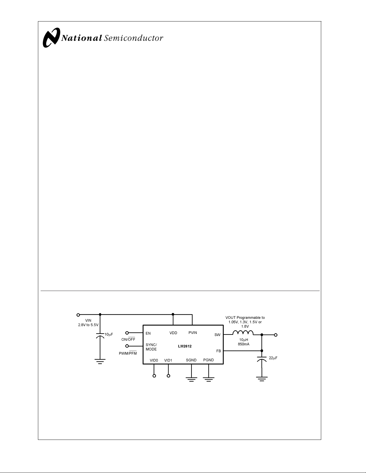
Typical Application Circuit
20007102
© 2002 National Semiconductor Corporation DS200071 www.national.com
Page 2

Connection Diagrams
LM2612
micro SMD package
TOP VIEW
20007104
BOTTOM VIEW
20007105
Ordering Information
Order Number Package Type NSC Package
Drawing
10-Pin micro SMD
LM2612ABP
LM2612BBP 250 Units, Tape and Reel
LM2612ABPX 3000 Units, Tape and Reel
LM2612BBPX 3000 Units, Tape and Reel
10-bump Wafer Level Chip Scale
(micro SMD)
BPA10VWB
250 Units, Tape and Reel
Supplied As
Pin Description
Pin Number(*) Pin Name Function
A1 FB Feedback Analog Input. Connect to the output at the output filter capacitor (Figure 1)
B1 VID1 Output Voltage Control Inputs. Set the output voltage using these digital inputs (see Table
C1 VID0
D1 SYNC/MODE Synchronization Input. Use this digital input for frequency selection or modulation control.
D2 EN Enable Input. Set this CMOS Schmitt trigger digital input high to VDD for normal
D3 PGND Power Ground
C3 SW Switching Node connection to the internal PFET switch and NFET synchronous rectifier.
B3 PVIN Power Supply Input to the internal PFET switch. Connect to the input filter capacitor
A3 VDD Analog Supply Input. If board layout is not optimum, an optional 0.1µF ceramic capacitor
A2 SGND Analog and Control Ground
(*) note the pin numbering scheme for the MicroSMD package was revised in April, 2002 to comform to JEDEC standard. Only the pin numbers were revised. No
changes to the physical location of the inputs/outputs were made. For reference purpose, the obsolete numbering has FB as pin 1, VID1 as pin 2, VID0 as pin3,
SYNC as pin 4, EN as pin 5, PGND as pin 6, SW as pin 7, PVIN as pin 8, VDD as pin 9 and SGND as pin 10.
1). The output defaults to 1.5V if these pins are unconnected.
Set:
SYNC/MODE = high for low-noise 600kHz PWM mode
SYNC/MODE = low for low-current PFM mode
SYNC/MODE = a 500kHz - 1MHz external clock for synchronization to an external clock in
PWM mode. See
operation. For shutdown, set low to SGND. Set EN low during power-up and other low
supply voltage conditions. (See
Connect to an inductor with a saturation current rating that exceeds the 850mA max
Switch Peak Current Limit specification of the LM2612 (
(
Figure 1
is suggested (
).
Synchronization and Operating Modes
Shutdown Mode
Figure 1
)
in the
in the
Device Information
Figure 1
Device Information
section.)
)
section.
www.national.com 2
Page 3

LM2612
Absolute Maximum Ratings (Note 1)
If Military/Aerospace specified devices are required,
please contact the National Semiconductor Sales Office/
Distributors for availability and specifications.
PVIN, VDD, to SGND −0.2V to +6V
PGND to SGND −0.2V to +0.2V
EN, SYNC/MODE, VID0, VID1 to
SGND −0.2V to +6V
Lead temperature
(Soldering, 10 sec.) 260˚C
Junction Temperature (Note 2) −25˚C to 125˚C
Minimum ESD Rating
Human body model, C = 100pF, R =
1.5 kΩ
Thermal Resistance (θ
)
JA
±
2.5kV
LM2612ABP & LM2612BBP (Note 3) 170˚C/W
FB, SW (GND −0.2V) to
(VDD +0.2V)
Storage Temperature Range −45˚C to +150˚C
Electrical Characteristics
Specifications with standard typeface are for TA=TJ= 25˚C, and those in bold face type apply over the full Operating Temperature Range (T
0V.
Symbol Parameter Conditions Min Typ Max Units
V
V
V
IN
FB
HYST
Input Voltage Range (Note5)PVIN = VDD = VID1 = VIN,
Feedback Voltage
(Note 6)
PFM Comparator Hysteresis
Voltage
(Note 7)
I
SHDN
I
Q1
I
Q2
R
DSON (P)
Shutdown Supply Current EN = 0V 0.1 3 µA
DC Bias Current into VDD
(V
OUT
Pin-Pin Resistance for P
FET
R
DSON (N)
Pin-Pin Resistance for N
FET
R
DSON , TC
FET Resistance
Temperature Coefficient
I
lim
Switch Peak Current Limit
(Note 8)
V
EN_H
EN Positive Going
Threshold Voltage
(Note 8)
V
EN_L
EN Negative Going
Threshold Voltage
(Note 8)
V
SYNC_H
SYNC/MODE Positive
Going Threshold Voltage
V
SYNC_L
SYNC/MODE Negative
Going Threshold Voltage
V
ID_H
V
ID0,VID1
Threshold Voltage
V
ID_L
V
ID0,VID1
Threshold Voltage
= −25˚C to +85˚C). Unless otherwise specified, PVIN = VDD = EN = SYNC = 3.6V, VID0 = VID1 =
A=TJ
VID0 = 0V
VID0 = V
VID0 = V
, VID1 = V
IN
, VID1 = 0V 1.274 1.30 1.326
IN
IN
2.8 5.5 V
1.00 1.05 1.10
VID0 = 0V, VID1 = 0V 1.470 1.50 1.530
VID0 = 0V, VID1 = V
IN
1.764 1.8 1.836
PFM Mode (SYNC = 0V)
16 mV
set to 1.5V)
No-Load, PFM mode
(SYNC/MODE = 0V)
No-Load, PWM mode
(SYNC/MODE = V
)
IN
LM2612ABP & LM2612BBP
LM2612ABP & LM2612BBP
150 185
555 725
370 500 mΩ
330 500 mΩ
0.5 %/C
LM2612ABP 510 690 850
LM2612BBP 400 690 980
= 3.6V
V
DD
2.54 2.85 V
= 3.6V
V
DD
1.70 2.00 V
0.95 1.3 V
0.4 0.9 V
Positive Going
Negative Going
0.4 0.83 V
0.92 1.2 V
V
µA
mA
www.national.com3
Page 4

Electrical Characteristics (Continued)
Specifications with standard typeface are for TA=TJ= 25˚C, and those in bold face type apply over the full Operating Tem-
LM2612
perature Range (T
0V.
Symbol Parameter Conditions Min Typ Max Units
I
VID
VID1, VID0 Pull Down
Current
f
sync
SYNC/MODE Clock
Frequency Range
(Note 10)
F
OSC
Internal Oscillator
Frequency
T
min
Minimum ON-Time of P FET
Switch in PWM Mode
Load Transient Response in
PWM Mode
Line Transient Response in
PFM Mode
Note 1: Absolute Maximum Ratings indicate limits beyond which damage to the device may occur. Operating Ratings are conditions for which the device is intended
to be functional, but parameter specifications may not be guaranteed. For guaranteed specifications and associated test conditions, see the Min and Max limits and
Conditions in the Electrical Characteristics table. Electrical Characteristics table limits are guaranteed by production testing, design or correlation using standard
Statistical Quality Control methods. Typical (Typ) specifications are mean or average values from characterization at 25C and are not guaranteed.
Note 2: In PWM mode, Thermal shutdown will occur if the junction temperature exceeds the 150˚C maximum junction temperature of the device.
Note 3: Thermal resistance specified with 2 layer PCB(0.5/0.5 oz. cu).
Note 4: Thermal resistance specified with 3 layer PCB (2/1/1 oz. cu) and 12 vias 0.33mm diameter (see Application Note AN-1187).
Note 5: The LM2612 is designed for cell phone applications where turn-on after power-up is controlled by the system processor and internal UVLO (Under Voltage
LockOut) circuitry is unecessary. The LM2612 has no UVLO circuitry and should be kept in shutdown by holding the EN pin low until the input voltage exceeds 2.8V.
Although the LM2612 exhibited safe behavior during pre-production evaluation while enabled at low input voltages, this is not guaranteed.
Note 6: The feedback voltage is trimmed at the 1.5V output setting. The other output voltages result from the pin selection of the internal DAC’s divider ratios. The
precision for the feedback voltages is
if trimming at other voltages is desired.
Note 7: : The hysteresis voltage is the minimum voltage swing on FB that causes the internal feedback and control circuitry to turn the internal PFET switch on and
then off, during PFM mode.
Note 8: Current limit is built-in, fixed, and not adjustable. If the current limit is reached while the output is pulled below about 0.7V, the internal PFET switch turns
off for 2.5 µs to allow the inductor current to diminish.
Note 9: EN is a CMOS Schmitt trigger digital input with logic thresholds that scale with the supply voltage at the VDD pin. The nominal logic thresholds are
approximately 0.71VDD and 0.55VDD for the high and low thresholds respectively.
Note 10: SYNC driven with an external clock switching between V
external clock frequency. The LM2612 synchronizes to the rising edge of the external clock.
= −25˚C to +85˚C). Unless otherwise specified, PVIN = VDD = EN = SYNC = 3.6V, VID0 = VID1 =
A=TJ
VID1, VID0 = 3.6V
1.8 µA
500 1000 kHz
LM2612ABP, PWM Mode
(SYNC = VIN)
LM2612BBP, PWM Mode
(SYNC = VIN)
468 600 732
450 600 750
200 ns
Circuit of
I
OUT
Circuit of
VIN= 3.0V to 3.6V Step
t
r=tp
±
2%, except for the 1.05V setting, which is 5%. Contact the Portable Power Applications group at National Semiconductor,
Figure 1
= 20mA to 200mA Step
±
25 mV
Figure 1
±
3mV
=10µs
and GND. When an external clock is present at SYNC, the IC is forced to PWM mode at the
IN
kHz
www.national.com 4
Page 5
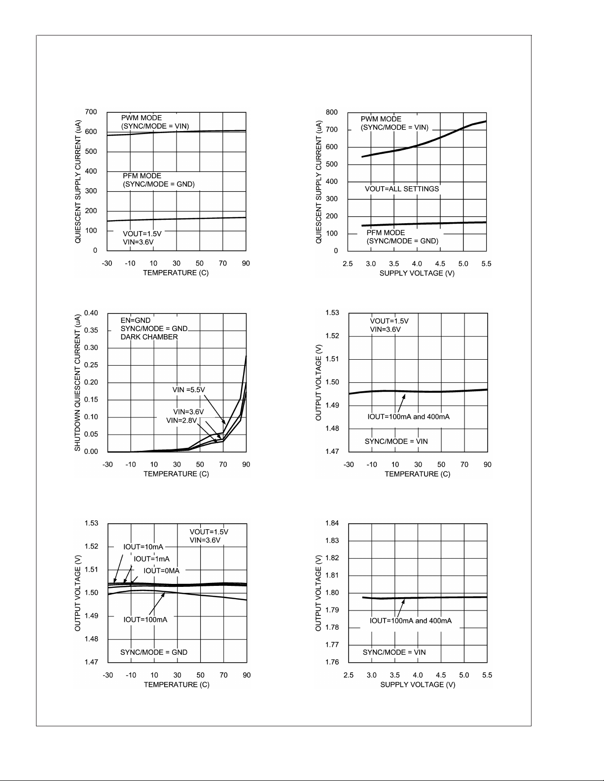
Typical Operating Characteristics
LM2612ABP, Circuit of
L
= 10 µH, unless otherwise noted.
1
Quiescent Supply Current vs Temperature Quiescent Supply Current vs Supply Voltage
Shutdown Quiescent Current vs Temperature Output Voltage vs Temperature (PWM Mode)
Figure 1
,VIN= 3.6V, TA= 25˚C,
20007106 20007107
LM2612
20007108
Output Voltage vs Temperature (PFM Mode)
20007110 20007111
Output Voltage vs Supply Voltage
(V
= 1.8V, PWM Mode)
OUT
20007109
www.national.com5
Page 6
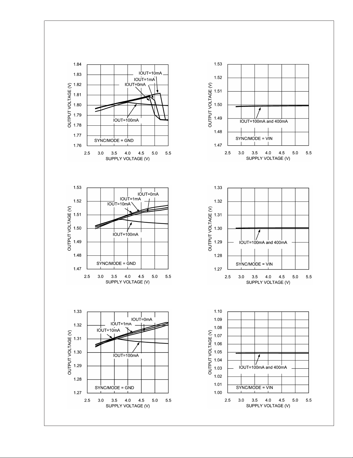
Typical Operating Characteristics LM2612ABP, Circuit of
µH, unless otherwise noted. (Continued)
LM2612
Output Voltage vs Supply Voltage
(V
= 1.8V, PFM Mode)
OUT
20007112 20007113
Output Voltage vs Supply Voltage
(V
= 1.5V, PFM Mode)
OUT
Figure 1
,VIN= 3.6V, TA= 25˚C, L1=10
Output Voltage vs Supply Voltage
(V
= 1.5V, PWM Mode)
OUT
Output Voltage vs Supply Voltage
(V
= 1.3V, PWM Mode)
OUT
20007114
Output Voltage vs Supply Voltage
(V
= 1.3V, PFM Mode)
OUT
20007116 20007117
www.national.com 6
Output Voltage vs Supply Voltage
(V
= 1.05V, PWM Mode)
OUT
20007115
Page 7

LM2612
Typical Operating Characteristics LM2612ABP, Circuit of
µH, unless otherwise noted. (Continued)
Output Voltage vs Supply Voltage
(V
= 1.05V, PFM Mode)
OUT
Output Voltage vs Output Current
(V
= 1.8V, PFM Mode)
OUT
20007118
Output Voltage vs Output Current
Output Voltage vs Output Current
Figure 1
(V
(V
,VIN= 3.6V, TA= 25˚C, L1=10
= 1.8V, PWM Mode)
OUT
= 1.5V, PWM Mode)
OUT
20007119
Output Voltage vs Output Current
(V
= 1.5V, PFM Modee)
OUT
20007120
20007122
Output Voltage vs Output Current
(V
= 1.3V, PWM Mode)
OUT
20007121
20007123
www.national.com7
Page 8

Typical Operating Characteristics LM2612ABP, Circuit of
µH, unless otherwise noted. (Continued)
LM2612
Output Voltage vs Output Current
(V
= 1.3V, PFM Mode)
OUT
20007124 20007125
Output Voltage vs Output Current
(V
= 1.05V, PFM Mode, With Diode)
OUT
Figure 1
,VIN= 3.6V, TA= 25˚C, L1=10
Output Voltage vs Output Current
(V
= 1.05V, PWM Mode, With Diode)
OUT
Efficiency vs Output Current
(V
= 1.8V, PWM Mode, With Diode)
OUT
20007126 20007127
Efficiency vs Output Current
(V
= 1.8V, PFM Mode, With Diode)
OUT
20007128 20007129
www.national.com 8
Efficiency vs Output Current
(V
= 1.5V, PWM Mode, With Diode)
OUT
Page 9

LM2612
Typical Operating Characteristics LM2612ABP, Circuit of
µH, unless otherwise noted. (Continued)
Efficiency vs Output Current
(V
= 1.5V, PFM Mode, With Diode)
OUT
Efficiency vs Output Current
(V
= 1.3V, PFM Mode)
OUT
20007130 20007131
(V
OUT
Figure 1
,VIN= 3.6V, TA= 25˚C, L1=10
Efficiency vs Output Current
= 1.3V, PWM Mode, With Diode)
Efficiency vs Output Current
(V
= 1.05V, PWM Mode)
OUT
Efficiency vs Output Current
(V
= 1.05V, PFM Mode, With Diode)
OUT
20007132
20007134
Efficiency vs Output Current
(V
= 1.8V, PWM Mode,No Diode)
OUT
20007133
20007135
www.national.com9
Page 10

Typical Operating Characteristics LM2612ABP, Circuit of
µH, unless otherwise noted. (Continued)
LM2612
Efficiency vs Output Current
(V
= 1.8V, PFM Mode, No Diode)
OUT
Figure 1
,VIN= 3.6V, TA= 25˚C, L1=10
Switching Frquency vs Temperature
(PWM Mode)
Load Transient Response (PWM Mode) Load Transient Response (PFM Mode)
A: INDUCTOR CURRENT, 500mA/div
B: SW PIN, 5V/div
C: V
, 50mV/div, AC COUPLED
OUT
D: LOAD, 20mA to 200mA, 200mA/div
Shutdown Response (PWM Mode) Shutdown Response (PFM Mode)
20007141
20007136
A: INDUCTOR CURRENT, 500mA/div
B: SW PIN, 5V/div
C: V
, 50mV/div, AC COUPLED
OUT
D: LOAD, 10mA to 100mA, 100mA/div
20007139
20007146
A: INDUCTOR CURRENT, 500mA/div
B: SW PIN, 2V/div
C: V
, 1V/div
OUT
D: EN, 5V/div
20007140
www.national.com 10
A: INDUCTOR CURRENT, 500mA/div
B: SW PIN, 2V/div
C: V
, 1V/div
OUT
D: EN, 5V/div
20007145
Page 11

LM2612
Typical Operating Characteristics LM2612ABP, Circuit of
µH, unless otherwise noted. (Continued)
PWM to PFM Response Line Transient Response (PWM Mode)
A: INDUCTOR CURRENT, 500mA/div
B: SW PIN, 2V/div
C: V
, 50mV/div, AC COUPLED
OUT
D: SYNC/MODE, 5V/div
20007144
A: SUPPLY VOLTAGE, 500mV/div, AC COUPLED
B: SW PIN, 5V/div
C: V
, 10mV/div, AC COUPLED
OUT
L
=22µH
1
Figure 1
,VIN= 3.6V, TA= 25˚C, L1=10
20007149
www.national.com11
Page 12

Device Information
The LM2612 is a simple, step-down DC-DC converter opti-
LM2612
mized for powering low-voltage CPUs or DSPs in cell
phones and other miniature battery powered devices. It provides pin-selectable output voltages of 1.05V, 1.3V, 1.5V or
1.8V from a single 2.8V to 5.5V LiION battery cell. It is
designed for a maximum load capability of 400mA (300mA
for B grade).
The device has all three of the pin-selectable operating
modes required for cell phones and other complex portable
devices. Such applications typically spend a small portion of
their time operating at full power. During full power operation,
synchronized or fixed-frequency PWM mode offers full output current capability while minimizing interference to sensitive IF and data acquisition circuits. PWM mode uses synchronous rectification for high efficiency: typically 91% for a
100mA load with 1.8V output, 2.8V input. These applications
spend the remainder of their time in low-current standby
operation or shutdown to conserve battery power. During
standby operation, hysteretic PFM mode reduces quiescent
current to 150µA typ to maximize battery life. Shutdown
mode turns the device off and reduces battery consumption
to 0.1µA (typ.).
The LM2612 offers good performance and a full set of features. It is based on a current-mode switching buck
architecture for cycle-by-cycle current limiting. DC PWM
mode output voltage precision is
ages and
external clock between 500kHz and 1MHz. The output voltage selection pins eliminate external feedback resistors.
Additional features include soft-start, current overload protection, over-voltage protection and thermal overload protection.
The LM2612 is constructed using a chip-scale 10-pin micro
SMD package. The micro SMD package offers the smallest
possible size for space critical applications, such as cell
phones. Required external components are only a small
10uH inductor, and tiny 10uF and 22uF ceramic capacitors
for reduced board area.
±
3% for 1.05V.The SYNC/MODE input accepts an
±
2% for most output volt-
FIGURE 1. Typical Operating Circuit
Circuit Operation
Referring to
operates as follows: During the first part of each switching
cycle, the control block in the LM2612 turns on the internal
PFET switch. This allows current to flow from the input
through the inductor to the output filter capacitor and load.
The inductor limits the current to a ramp with a slope of (V
-V
OUT
second part of each cycle, the controller turns the PFET
switch off, blocking current flow from the input, and then
turns the NFET synchronous rectifier on. In response, the
inductor’s magnetic field collapses, generating a voltage that
forces current from ground through the synchronous rectifier
to the output filter capacitor and load. As the stored energy is
www.national.com 12
Figure 1,Figure 2
)/L, by storing energy in a magnetic field. During the
, and
Figure 3
the LM2612
IN
20007103
transferred back into the circuit and depleted, the inductor
current ramps down with a slope of V
current reaches zero before the next cycle, the synchronous
rectifier is turned off to prevent current reversal. The output
filter capacitor stores charge when the inductor current is
high, and releases it when low,smoothing the voltage across
the load.
The output voltage is regulated by modulating the PFET
switch on-time to control the average current sent to the
load. The effect is identical to sending a duty-cycle modulated rectangular wave formed by the switch and synchronous rectifier to a low-pass filter created by the inductor and
output filter capacitor. The output voltage is equal to the
average voltage at the SW pin.
/L. If the inductor
OUT
Page 13

Circuit Operation (Continued)
LM2612
20007101
FIGURE 2. Simplified Functional Diagram
PWM Operation
The LM2612 can be set to current-mode PWM operation by
connecting the SYNC/MODE pin to VDD. While in PWM
(Pulse Width Modulation) mode, the output voltage is regulated by switching at a constant frequency and then modulating the energy per cycle to control power to the load.
Energy per cycle is set by modulating the PFET switch
on-time pulse-width to control the peak inductor current. This
is done by controlling the PFET switch using a flip-flop driven
by an oscillator and a comparator that compares a ramp
from the current-sense amplifier with an error signal from a
voltage-feedback error amplifier. At the beginning of each
cycle, the oscillator sets the flip-flop and turns on the PFET
switch, causing the inductor current to ramp up. When the
current sense signal ramps past the error amplifier signal,
the PWM comparator resets the flip-flop and turns off the
PFET switch, ending the first part of the cycle. The NFET
synchronous rectifier turns on until the next clock pulse or
the inductor current ramps to zero. If an increase in load
pulls the output voltage down, the error amplifier output
increases, which allows the inductor current to ramp higher
before the comparator turns off the PFET switch. This increases the average current sent to the output and adjusts
for the increase in the load.
Before going to the PWM comparator, the current sense
signal is summed with a slope compensation ramp from the
oscillator for stability of the current feedback loop. During the
second part of the cycle, a zero crossing detector turns off
the NFET synchronous rectifier if the inductor current ramps
to zero.
www.national.com13
Page 14

PWM Operation (Continued)
LM2612
PWM Mode Switching Waveform PFM Mode Switching Waveform
A: INDUCTOR CURRENT, 500mA/div
B: SW PIN, 2V/div
C: V
, 10mV/div, AC COUPLED
OUT
FIGURE 3. Typical Circuit Waveforms in (a) PWM Mode and (b) PFM Mode
20007143
PFM Operation
Connecting the SYNC/MODE pin to SGND sets the LM2612
to hysteretic PFM operation. While in PFM (Pulse Frequency
Modulation) mode, the output voltage is regulated by switching with a discrete energy per cycle and then modulating the
cycle rate, or frequency, to control power to the load. This is
done by using an error comparator to sense the output
voltage and control the PFET switch. The device waits as the
load discharges the output filter capacitor, until the output
voltage drops below the lower threshold of the PFM errorcomparator. Then the error comparator initiates a cycle by
turning on the PFET switch. This allows current to flow from
the input, through the inductor to the output, charging the
output filter capacitor. The PFET switch is turned off when
the output voltage rises above the regulation threshold of the
PFM error comparator. After the PFET switch turns off, the
output voltage rises a little higher as the inductor transfers
stored energy to the output capacitor by pushing current into
the output cacitor. Thus, the output voltage ripple in PFM
mode is proportional to the hysteresis of the error comparator and the inductor current.
In PFM mode, the device only switches as needed to service
the load.This lowers current consumption by reducing power
consumed during the switching action in the circuit due to
transition losses in the internal MOSFETs, gate drive currents, eddy current losses in the inductor, etc. It also improves light-load voltage regulation. During the second part
of the cycle, the intrinsic body diode of the NFET synchronous rectifier conducts until the inductor current ramps to
zero. The LM2612 does not turn on the synchronous rectifier
while in PFM mode.
Operating Mode Selection (SYNC/MODE Pin)
The SYNC/MODE digital input pin is used to select between
PWM or PFM operating modes. Set SYNC/MODE high
(above 1.3V) for 600kHz PWM operation when the system is
active and the load is above 50mA. Set SYNC/MODE low
(below 0.4V) to select PFM mode when the load is less than
A: INDUCTOR CURRENT, 500mA/div
B: SW PIN, 2V/div
C: V
, 50mV/div, AC COUPLED
OUT
50mA for precise regulation and reduced current consumption when the system is in standby.The LM2612 has an
over-voltage protection feature that may activate if the device is left in PWM mode under low-load conditions (
to prevent the output voltage from rising too high. See
ervoltage Protection
Select modes with the SYNC/MODE pin using a signal with
a slew rate faster than 5V/100µs. Use a comparator Schmitt
trigger or logic gate to drive the SYNC/MODE pin. Do not
leave the pin floating of allow it to linger between logic levels.
These measures will prevent output voltage errors that could
otherwise occur in response to an indeterminate logic state.
Ensure a minimum load to keep the output voltage in regulation when switching modes frequently. The minimum load
requirement varies depending on the mode change frequency. A typical load of 8µA is required when modes are
changed at 100 ms intervals, 85µA for 10 ms and 800µA for
1 ms.
, for more information.
20007142
<
50mA)
Frequency Synchronization (SYNC/MODE Pin)
The SYNC/MODE input can also be used for frequency
synchronization. To synchronize the LM2612 to an external
clock, supply a digital signal to the SYNC/MODE pin with a
voltage swing exceeding 0.4V to 1.3V. During synchronization, the LM2612 initiates cycles on the rising edge of the
clock. When synchronized to an external clock, it operates in
PWM mode. The device can synchronize to a 50%
duty-cycle clock over frequencies from 500kHz to 1MHz.
Use the following waveform and duty-cycle guidelines when
applying an external clock to the SYNC/MODE pin. Each
clock cycle should have high and low periods between 1.3µs
and 200ns and a duty cycle between 30% and 70%. The
total clock period should be 2µs or less. Clock under/
overshoot should be less than 100mV below GND or above
V
. When applying noisy clock signals, especially sharp
DD
edged signals from a long cable during evaluation, terminate
the cable at its characteristic impedance; add an RC filter to
the SYNC pin, if necessary, to soften the slew rate and
Ov-
www.national.com 14
Page 15

Frequency Synchronization
(SYNC/MODE Pin)
over/undershoot. Note that sharp edged signals from a pulse
or function generator can develop under/overshoot as high
as 10V at the end of an improperly terminated cable.
Drive the SYNC/MODE pin using a signal with a slew rate
faster than 5V/100µs. Use a comparator Schmitt trigger or
logic gate to drive the SYNC/MODE pin. Do not leave the pin
floating of allow it to linger between logic levels. These
measures will prevent output voltage errors that could otherwise occur in response to an indeterminate logic state.
(Continued)
Overvoltage Protection
The LM2612 has an over-voltage comparator that prevents
the output voltage from rising too high when the device is left
in PWM mode under low-load conditions. Otherwise, the
output voltage could rise out of regulation from the minimum
energy transferred per cycle due to the 200ns minimum
on-time of the PFET switch while in PWM mode. When the
output voltage rises by 30mV over its regulation threshold,
the OVP comparator inhibits PWM operation to skip pulses
until the output voltage returns to the regulation threshold. In
over voltage protection, output voltage and ripple increase
slightly.
Shutdown Mode
Setting the EN digital input pin low to SGND places the
LM2612 in a 0.1uA (typ) shutdown mode. During shutdown,
the PFET switch, NFET synchronous rectifier, reference,
control and bias of the LM2612 are turned off. Setting EN
high to VDD enables normal operation. While turning on, soft
start is activated. EN is a CMOS Schmitt trigger digital input
with thresholds that scale with the input voltage at VDD. The
nominal logic thresholds are approximately 0.71VDD and
0.55VDD for the high and low thresholds respectively. Drive
EN using CMOS logic referenced to the supply voltage at the
VDD pin of the LM2612.
EN must be set low to turn off the LM2612 during power-up
and undervoltage conditions when the supply is less than the
2.8V minimum operating voltage. The LM2612 is designed
for mobile phones and similar applications where power
sequencing is determined by the system controller and internal UVLO (Under Voltage LockOut) circuitry is unnecessary. The LM2612 has no UVLO circuitry. Although the
LM2612 exhibited safe behavior during pre-production
evaluation while enabled at low input voltages, this is not
guaranteed.
Internal Synchronous Rectification
While in PWM mode, the LM2612 uses an internal NFET as
a synchronous rectifier to improve efficiency by reducing
rectifier forward voltage drop and associated power loss. In
general, synchronous rectification provides a significant improvement in efficiency whenever the output voltage is relatively low compared to the voltage drop across an ordinary
rectifier diode.
Under moderate and heavy loads, the internal NFET synchronous rectifier is turned on during the inductor current
down-slope in the second part of each cycle. The synchronous rectifier is turned off prior to the next cycle, or when the
inductor current ramps near zero at light loads. The NFET is
designed to conduct through it’s intrinsic body diode during
transient intervals before it turns on, eliminating the need for
an external diode.
Synchronous rectification is disabled and the NFET conducts through it’s body diode during the second part of each
cycle while in PFM mode to reduce quiescent current associated with the synchronous rectifier’s control circuitry. The
synchronous rectifier may also remain off in PWM mode
when duty cycles are short due to high input-output voltage
differentials or light loads, when there is insufficient time for
the synchronous rectifier to activate. The body diode of the
NFET is also used under these conditions. To increase efficiency in PFM or short duty-cycle PWM conditions, place an
external Schottky diode from PGND to SW. Contact the
Portable Power applications group at National Semiconductor, if interested in a device with synchronous rectification in
PFM mode.
Current Limiting
Acurrent limit feature allows the LM2612 to protect itself and
external components during overload conditions. Current
limiting is implemented using an independent internal comparator that trips at 850mA max, (980mA for B grade devices). In PWM mode, cycle-by-cycle current limiting is normally used. If an excessive load pulls the output voltage
down to approximately 0.7V, then the device switches to a
timed current limit mode. In timed current limit mode the
internal P-FET switch is turned off after the current comparator trips and the beginning of the next cycle is inhibited for
2.5µs to force the instantaneous inductor current to ramp
down to a safe value. PFM mode also uses timed current
limit operation. The synchronous rectifier is off in timed current limit mode. Timed current limit prevents the loss of
current control seen in some products when the output voltage is pulled low in serious overload conditions.
Current Limiting and PWM Mode Transient Response Considerations
The LM2612 was designed for fast response to moderate
load steps. Harsh transient conditions during loads above
300mA can cause the inductor current to swing up to the
850mA current limit, resulting in PWM mode jitter or instability from activation of the current limit comparator. To avoid
this jitter or instability, do not power-up or start the LM2612
into a full load (loads near or above 400mA). Do not change
operating modes or output voltages when operating at a full
load. Avoid extremely sharp and wide-ranging load steps to
full load, such as from
<
30mA to>350mA.
Pin Selectable Output Voltage
The LM2612 features pin-selectable output voltage to eliminate the need for external feedback resistors. The output
can be set to 1.05V, 1.3V, 1.5V or 1.8V by configuring the
VID0 and VID1 pins. See
Application Information
Setting the Output Voltage
section for further details.
in the
Soft-Start
The LM2612 has soft start to reduce current inrush during
power-up and startup. This reduces stress on the LM2612
and external components. It also reduces startup transients
on the power source.
LM2612
www.national.com15
Page 16

Soft-Start (Continued)
Soft start is implemented by ramping up the internal refer-
LM2612
ence in the LM2612 to gradually increase the output voltage.
The reference ramps up in about 400µs. When powering up
in PWM mode, soft start may take an additional 200us to
allow time for the error amplifier compensation network to
charge.
Thermal Overload Protection
The LM2612 has a thermal overload protection function that
operates to protect itself from short-term misuse and overload conditions. When the junction temperature exceeds
about 155˚C, the device initiates a soft-start cycle which is
completed after the temperature drops below 130˚C. Prolonged operation in thermal overload conditions may damage the device and is considered bad practice.
Application Information
Setting The Output Voltage
The LM2612 features pin-selectable output voltage to eliminate the need for external feedback resistors. Select an
output voltage of 1.05V, 1.3V,1.5V or 1.8V by configuring the
VID0 and VID1 pins, as directed in
Model Vendor Phone FAX
DO1608C-103 Coilcraft 847-639-6400 847-639-1469
DO1606T-103 Coilcraft
UP1B-100 Coiltronics 561-241-7876 561-241-9339
UP0.4CB-100 Coiltronics
ELL6GM100M Panasonic 714-373-7366 714-373-7323
ELL6PM100M Panasonic
P1174.103T Pulse Engineering 858-674-8100 858-674-8262
CDRH5D18-100 Sumida 847-956-0666 847-956-0702
CDRH4D28-100 Sumida
CDC5D23-100 Sumida
NP05D B100M Taiyo Yuden 847-925-0888 847-925-0899
NP04S B100N Taiyo Yuden
SLF6025T-100M1R0 TDK 847-803-6100 847-803-6296
SLF6020T-100MR90 TDK
A918CY-100M Toko 847-297-0070 847-699-7864
A915AY-100M Toko
Table 1
.
TABLE 2. Suggested Inductors and Their Suppliers
TABLE 1. VID0 and VID1 Output Voltage Selection
Settings
V
(V) Logic Level
OUT
VID0 VID1
1.8 0 1
1.5 0 0
1.5 N.C. N.C.
1.3 1 0
1.05 1 1
VID0 and VID1 are digital inputs. They may be set high by
connecting to VDD or low by connecting to SGND. Optionally, VID0 and VID1 may be driven by digital gates that
provide over 1.2V for a high state and less than 0.4V for a
low state to ensure valid logic levels. The VID0 and VID1
inputs each have an internal 1.8 µA pull-down that pulls them
low for a default 1.5V output, when left unconnected. Leaving these pins open is acceptable, but setting the pins high or
low is recommended.
Inductor Selection
A 10µH inductor with a saturation current rating over 850mA
(980mA for B grade) is recommended for most applications.
The inductor’s resistance should be less than 0.3Ω for good
efficiency.
Table 2
lists suggested inductors and suppliers.
For low-cost applications, an unshielded bobbin inductor is
suggested. For noise critical applications, a toroidal or
shielded-bobbin inductor should be used. A good practice is
to lay out the board with overlapping footprints of both types
for design flexibility. This allows substitution of a low-noise
toroidal inductor,in the event that noise from low-cost bobbin
models is unacceptable.
The saturation current rating is the current level beyond
which an inductor looses it’s inductance. Beyond this rating,
TABLE 3. Suggested Capacitors and Their Suppliers
Model Size Vendor Phone FAX
22µF, X7R or X5R Ceramic Capacitor for C2 (Output Filter Capacitor)
C3225X5RIA226M 1210 TDK 847-803-6100 847-803-6296
www.national.com 16
the inductor looses it’s ability to limit current through the
PFET switch to a ramp and allows the switch current to
increase rapidly. This can cause poor efficiency, regulation
errors or stress to DC-DC converters like the LM2612. Saturation occurs when the magnetic flux density from current
through the windings of the inductor exceeds what the inductor’s core material can support with energy storage in a
corresponding magnetic field.
Page 17

Application Information (Continued)
TABLE 3. Suggested Capacitors and Their Suppliers (Continued)
Model Size Vendor Phone FAX
JMK325BJ226MM 1210 Taiyo-Yuden 847-925-0888 847-925-0899
ECJ4YB0J226M 1210 Panasonic 714-373-7366 714-373-7323
GRM42-2X5R226K6.3 1210 muRata 404-436-1300 404-436-3030
10µF, 6.3V, X7R or X5R Ceramic Capacitor for C1 (Input Filter Capacitor)
C2012X5R0J106M 0805 TDK 847-803-6100 847-803-6296
JMK212BJ106MG 0805 Taiyo
Yuden
ECJ3YB0J106K 1206 Panasonic 714-373-7366 714-373-7323
GRM40X5R106K6.3 0805 muRata 404-436-1400 404-436-3030
847-925-0888 847-925-0899
LM2612
Capacitor Selection
Use a 10µF, 6.3V, X7R or X5R ceramic input filter capacitor
and a 22uF, X7R or X5R ceramic output filter capacitor.
These provide an optimal balance between small size, cost,
reliability and performance. Do not use Y5V ceramic capacitors.
Table 3
A 10µF ceramic capacitor can be used for the output filter
capacitor for smaller size in applications where the
worst-case transient load step is less than 200mA. Use of a
10µF output capacitor trades off smaller size for an increase
in output voltage ripple, and undershoot during line and load
transient response.
The input filter capacitor supplies current to the PFET switch
of the LM2612 in the first part of each cycle and reduces
voltage ripple imposed on the input power source. The output filter capacitor smoothes out current flow from the inductor to the load, helps maintain a steady output voltage during
transient load changes and reduces output voltage ripple.
These capacitors must be selected with sufficient capacitance and sufficiently low ESR to perform these functions.
The ESR, or equivalent series resistance, of the filter capacitors is a major factor in voltage ripple. The contribution from
ESR to voltage ripple is around 75-95% for most electrolytic
capacitors and considerably less for ceramic capacitors. The
remainder of the ripple is from charge storage due to capacitance.
Diode Selection
An optional Schottky diode (D1 in Figure 1) can be added to
increase efficiency in PFM mode and light-load PWM mode.
This may be desired in applications where increased efficiency for improving operational battery life takes precedence over increased system size associated with the
Schottky diode. Typically, use of an external schottky diode
increases PFM mode efficiency from 72.7% to 85.0% (20
mAload, V
in the
Use a Schottky diode with a current rating higher than
850mA, such as an MBRM140T3. Use of a device rated for
30V or more reduces diode reverse leakage in high temperature applications.
Thermal Design
The LM2612 has a thermal overload protection feature
which activates when the junction temperature exceeds
around 155˚C, until the device cools to 130˚C. However,
running the device this hot continually may damage it and is
lists suggested capacitors and suppliers.
= 1.8V,VIN= 3.6V). See the efficiency curves
OUT
Typical Operating Characteristics
.
poor practice. Sufficient thermal design should be done to
keep the device below the specified 125˚C maximum operating junction temperature.
Micro SMD Package Assembly and Use
Use of the micro SMD package requires specialized board
layout, precision mounting and careful reflow techniques, as
detailed in National Semiconductor Application Note
AN-1112. Refer to the section
(SMT) Assembly Considerations
bly, alignment ordinals on the PC board should be used to
facilitate placement of the device. Since micro SMD packaging is a new technology, all layouts and assembly means
must be thoroughly tested prior to production. In particular,
proper placement, solder reflow and resistance to thermal
cycling must be verified.
The 10-Bump package used for the LM2612 has 170micron
solder balls and requires 6.7mil (6.7/1000 in.) pads for
mounting on the circuit board. The trace to each pad should
enter the pad with a 90˚ entry angle to prevent debris from
being caught in deep corners. Initially, the trace to each pad
should be 6 mil wide, for a section 6 mil long or longer, as a
thermal relief. Then each trace should neck up to its optimal
width over a span of 11 mils or more, so that the taper
extends beyond the edge of the package. The important
criterion is symmetry. This ensures the solder bumps on the
LM2612 re-flow evenly and that the device solders level to
the board. In particular, special attention must be paid to the
pads for bumps 6-9. Because PVIN and PGND are typically
connected to large copper planes, inadequate thermal reliefs
can result in late or inadequate reflow of these bumps.
The pad style used with micro SMD package must be the
NSMD (non-solder mask defined) type. This means that the
solder-mask opening is larger than the pad size or 9.7mils
for the LM2612. This prevents a lip that otherwise forms if
the solder-mask and pad overlap. This lip can hold the
device off the surface of the board and interfere with mounting. See Applications Note AN-1112 for specific instructions.
The micro SMD package is optimized for the smallest possible size in applications with red or infra-red opaque cases.
Because the micro SMD package lacks the plastic encapsulation characteristic of larger devices, it is vulnerable to light.
Back-side metalization and/or epoxy coating, along with
front-side shading by the printed circuit board, reduce this
sensitivity.However, the package has exposed die edges. In
particular,micro SMD devices are sensitive to light in the red
and Infrared range shining on the package’s exposed die
edges.
Surface Mount Technology
. For best results in assem-
www.national.com17
Page 18

Application Information (Continued)
Do not use or power-up the LM2612 while subjecting it to
LM2612
high intensity red or infrared light, otherwise degraded, unpredictable or erratic operation may result. Examples of light
sources with high red or infrared content include the sun and
halogen lamps. Package the circuit in a case opaque to red
or infrared light.
Board Layout Considerations
PC board layout is an important part of DC-DC converter
design. Poor board layout can disrupt the performance of a
DC-DC converter and surrounding circuitry by contributing to
EMI, ground bounce, and resistive voltage loss in the traces.
These can send erroneous signals to the DC-DC converter
IC, resulting in poor regulation or instability. Poor layout can
also result in reflow problems leading to poor solder joints
between the micro SMD package and board pads. Poor
solder joints can result in erratic or degraded performance.
Good layout for the LM2612 can be implemented by following a few simple design rules:
1. Place the LM2612 on 6.7mil pads for micro SMD package. As a thermal relief, connect to each pad with a 6mil
wide trace (micro SMD), 6mils long or longer, then incrementally increase each trace to its optimal width over
a span so that the taper extends beyond the edge of the
package. The important criterion is symmetry to ensure
re-flow occurs evenly (see
bly and Use
2. Place the LM2612, inductor and filter capacitors close
together and make the traces short. The traces between
these components carry relatively high switching currents and act as antennas. Following this rule reduces
radiated noise. Place the capacitors and inductor within
0.2in (5mm) of the LM2612.
3. Arrange the components so that the switching current
loops curl in the same direction. During the first part of
each cycle, current flows from the input filter capacitor,
through the LM2612 and inductor to the output filter
capacitor and back through ground, forming a current
).
Micro SMD Package Assem-
loop. In the second part of each cycle, current is pulled
up from ground, through the LM2612 by the inductor, to
the output filter capacitor and then back through ground,
forming a second current loop. Routing these loops so
the current curls in the same direction prevents magnetic field reversal between the two part-cycles and
reduces radiated noise.
4. Connect the ground pins of the LM2612 and filter capacitors together using generous component-side copper fill as a pseudo-ground plane. Then, connect this to
the ground-plane (if one is used) with several vias. This
reduces ground-plane noise by preventing the switching
currents from circulating through the ground plane. It
also reduces ground bounce at the LM2612 by giving it
a low-impedance ground connection.
5. Use wide traces between the power components and for
power connections to the DC-DC converter circuit. This
reduces voltage errors caused by resistive losses across
the traces.
6. Route noise sensitive traces, such as the voltage feedback path, away from noisy traces between the power
components. The voltage feedback trace must remain
close to the LM2612 circuit and should be direct but
should be routed away from to noisy components. This
reduces EMI radiated onto the DC-DC converter’s own
voltage feedback trace.
7. Place noise sensitive circuitry, such as radio IF blocks,
away from the DC-DC converter, CMOS digital blocks
and other noisy circuitry. Interference with
noise-sensitive circuitry in the system can be reduced
through distance.
In mobile phones, for example, a common practice is to
place the DC-DC converter on one corner of the board,
arrange the CMOS digital circuitry around it (since this also
generates noise), and then place sensitive preamplifiers and
IF stages on the diagonally opposing corner. Often, the
sensitive circuitry is shielded with a metal pan and power to
it is post-regulated to reduce conducted noise, using
low-dropout linear regulators, such as the LP2966.
www.national.com 18
Page 19

Physical Dimensions inches (millimeters)
unless otherwise noted
LM2612 400mA Sub-miniature, Programmable, Step-Down DC-DC Converter for Ultra Low-Voltage
Circuits
10-Bump micro SMD Package
NS Package Number BPA10
The dimensions for X1, X2 and X3 are as given:
X1 = 1.996 +/− 0.030mm
X2 = 2.504 +/− 0.030mm
X3 = 0.850 +/− 0.1mm
NOTES: UNLESS OTHERWISE SPECIFIED
1. EPOXY COATING
2. 63Sn/37Pb EUTECTIC BUMP
3. RECOMMEND NON-SOLDER MASK DEFINED LANDING PAD.
4. PIN 1 IS ESTABLISHED BY LOWER LEFT CORNER WITH RESPECT TO TEXT ORIENTATION. REMAINING PINS ARE NUMBERED COUNTER
CLOCKWISE.
5. XXX IN DRAWING NUMBER REPRESENTS PACKAGE SIZE VARIATION WHERE X1 IS PACKAGE WIDTH, X2 IS PACKAGE LENGTH AND X3 IS
PACKAGE HEIGHT.
6.NO JEDEC REGISTRATION AS OF SEPT. 2000.
LIFE SUPPORT POLICY
NATIONAL’S PRODUCTS ARE NOT AUTHORIZED FOR USE AS CRITICAL COMPONENTS IN LIFE SUPPORT
DEVICES OR SYSTEMS WITHOUT THE EXPRESS WRITTEN APPROVAL OF THE PRESIDENT AND GENERAL
COUNSEL OF NATIONAL SEMICONDUCTOR CORPORATION. As used herein:
1. Life support devices or systems are devices or
systems which, (a) are intended for surgical implant
into the body, or (b) support or sustain life, and
whose failure to perform when properly used in
accordance with instructions for use provided in the
2. A critical component is any component of a life
support device or system whose failure to perform
can be reasonably expected to cause the failure of
the life support device or system, or to affect its
safety or effectiveness.
labeling, can be reasonably expected to result in a
significant injury to the user.
National Semiconductor
Corporation
Americas
Email: support@nsc.com
www.national.com
National does not assume any responsibility for use of any circuitry described, no circuit patent licenses are implied and National reserves the right at any time without notice to change said circuitry and specifications.
National Semiconductor
Europe
Fax: +49 (0) 180-530 85 86
Email: europe.support@nsc.com
Deutsch Tel: +49 (0) 69 9508 6208
English Tel: +44 (0) 870 24 0 2171
Français Tel: +33 (0) 1 41 91 8790
National Semiconductor
Asia Pacific Customer
Response Group
Tel: 65-2544466
Fax: 65-2504466
Email: ap.support@nsc.com
National Semiconductor
Japan Ltd.
Tel: 81-3-5639-7560
Fax: 81-3-5639-7507
 Loading...