

Page 1
LM2591HV
SIMPLE SWITCHER
®
Power Converter 150 kHz 1A
Step-Down Voltage Regulator
General Description
The LM2591HV series of regulators are monolithic integrated circuits that provide all the active functions for a
step-down (buck) switching regulator, capable of driving a
1A load with excellent line and load regulation. These devices are available in fixed output voltages of 3.3V, 5V, and
an adjustable output version.
This series of switching regulators is similar to the
LM2590HV, but without some of the supervisory and performance features of the latter.
Requiring a minimum number of external components, these
regulators are simple to use and include internal frequency
compensation
fixed-frequency oscillator.
The LM2591HV operates at a switching frequency of 150
kHz thus allowing smaller sized filter components than what
would be needed with lower frequency switching regulators.
Available in a standard 5-lead TO-220 package with several
different lead bend options, and a 5-lead TO-263 Surface
mount package.
Other features include a guaranteed
put voltage under all conditions of input voltage and output
load conditions, and
ternal shutdown is included, featuring typically 90 µA
standby current. Self protection features include a two stage
†
, improved line and load specifications and a
±
4% tolerance on out-
±
15% on the oscillator frequency. Ex-
July 2003
current limit for the output switch and an over temperature
shutdown for complete protection under fault conditions.
Features
n 3.3V, 5V, and adjustable output versions
n Adjustable version output voltage range, 1.2V to 57V
±
4% max over line and load conditions
n Guaranteed 1A output load current
n Available in 5-pin TO-220 and TO-263 (surface mount)
Package
n Input voltage range up to 60V
n 150 kHz fixed frequency internal oscillator
n On/Off control
n Low power standby mode, I
n High Efficiency
n Thermal shutdown and current limit protection
typically 90 µA
Q
Applications
n Simple high-efficiency step-down (buck) regulator
n Efficient pre-regulator for linear regulators
n On-card switching regulators
n Positive to Negative converter
Note:†Patent Number 5,382,918.
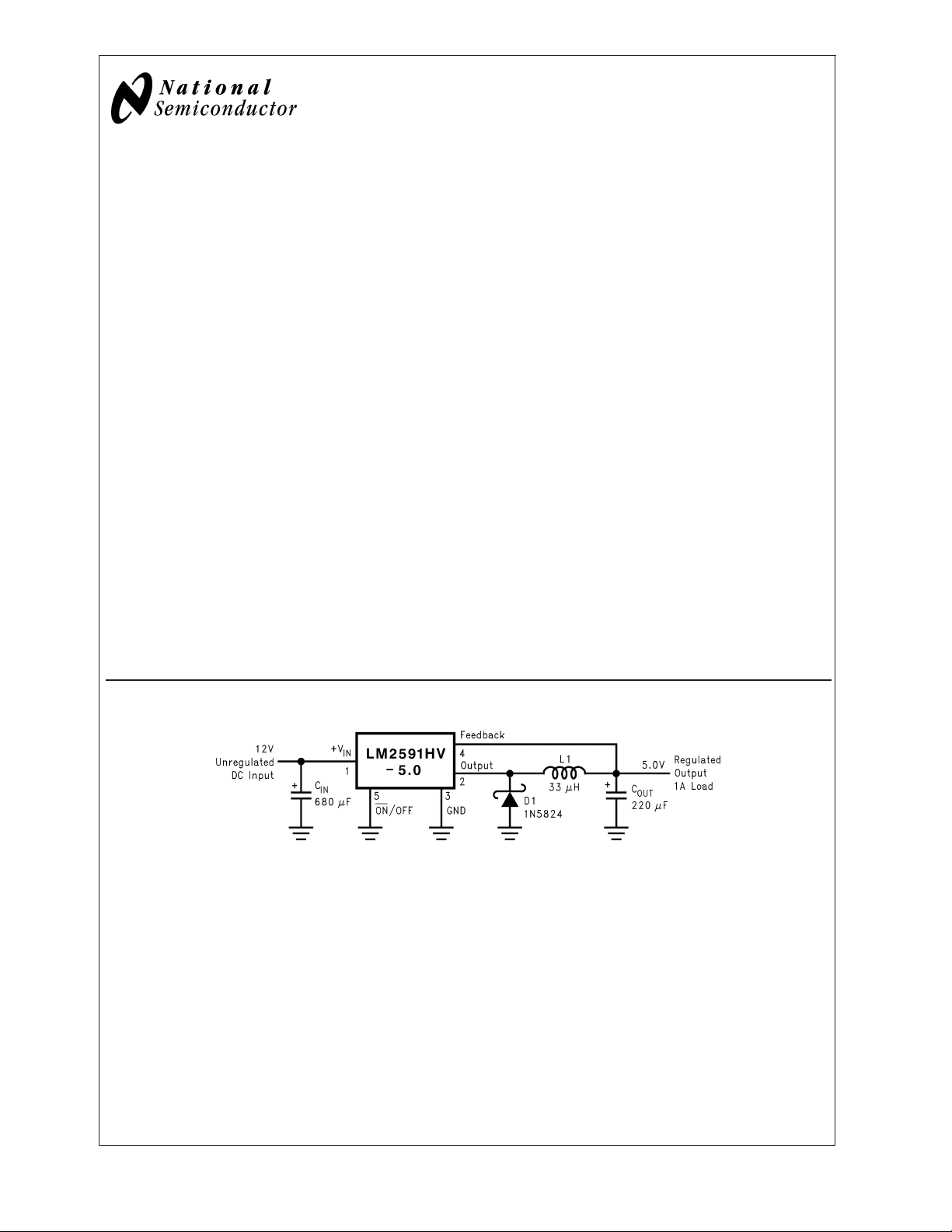
LM2591HV SIMPLE SWITCHER Power Converter 150 kHz 1A Step-Down Voltage Regulator
Typical Application (Fixed Output Voltage Versions)
10129301
SIMPLE SWITCHER®and Switchers Made Simple®are registered trademarks of National Semiconductor Corporation.
© 2003 National Semiconductor Corporation DS101293 www.national.com
Page 2
Absolute Maximum Ratings (Note 1)
If Military/Aerospace specified devices are required,
please contact the National Semiconductor Sales Office/
LM2591HV
Distributors for availability and specifications.
Maximum Supply Voltage (V
ON/OFF Pin Voltage
Feedback Pin Voltage −0.3 ≤ V ≤ +25V
) 63V
IN
−0.3 ≤ V ≤ +25V
Human Body Model (Note 2) 2 kV
Lead Temperature
S Package
Vapor Phase (60 sec.) +215˚C
Infrared (10 sec.) +245˚C
T Package (Soldering, 10 sec.) +260˚C
Maximum Junction Temperature +150˚C
Output Voltage to Ground
(Steady State) −1V
Operating Conditions
Power Dissipation Internally limited
Storage Temperature Range −65˚C to +150˚C
ESD Susceptibility
Temperature Range −40˚C ≤ TJ≤ +125˚C
Supply Voltage 4.5V to 60V
LM2591HV-3.3 Electrical Characteristics
Specifications with standard type face are for TJ= 25˚C, and those with boldface type apply over full Operating Temperature Range.
Symbol Parameter Conditions LM2591HV-3.3 Units
Typ Limit
(Note 3) (Note 4)
SYSTEM PARAMETERS (Note 5) Test Circuit Figure 1
V
OUT
Output Voltage 4.75V ≤ VIN≤ 60V, 0.2A ≤ I
η Efficiency V
= 12V, I
IN
=1A 77
LOAD
≤ 1A 3.3 V
LOAD
3.168/3.135 V(min)
3.432/3.465 V(max)
(Limits)
LM2591HV-5.0 Electrical Characteristics
Specifications with standard type face are for TJ= 25˚C, and those with boldface type apply over full Operating Temperature Range.
Symbol Parameter Conditions LM2591HV-5.0 Units
Typ Limit
(Limits)
(Note 3) (Note 4)
SYSTEM PARAMETERS (Note 5) Test Circuit Figure 1
V
OUT
Output Voltage 7V ≤ VIN≤ 60V, 0.2A ≤ I
≤ 1A 5 V
LOAD
4.800/4.750 V(min)
5.200/5.250 V(max)
η Efficiency V
= 12V, I
IN
=1A 82 %
LOAD
LM2591HV-ADJ Electrical Characteristics
Specifications with standard type face are for TJ= 25˚C, and those with boldface type apply over full Operating Temperature Range.
Symbol Parameter Conditions LM2591HV-ADJ Units
(Limits)
SYSTEM PARAMETERS (Note 5) Test Circuit Figure 1
V
FB
η Efficiency V
Feedback Voltage 4.5V ≤ VIN≤ 60V, 0.2A ≤ I
V
programmed for 3V. Circuit of Figure 1. 1.193/1.180 V(min)
OUT
= 12V, V
IN
OUT
= 3V, I
Typ Limit
(Note 3) (Note 4)
≤ 1A 1.230 V
LOAD
1.267/1.280 V(max)
=1A 76 %
LOAD
www.national.com 2
Page 3
All Output Voltage Versions Electrical Characteristics
Specifications with standard type face are for TJ= 25˚C, and those with boldface type apply over full Operating Temperature Range. Unless otherwise specified, V
= 12V for the 3.3V, 5V, and Adjustable version. I
IN
Symbol Parameter Conditions LM2591HV-XX Units
DEVICE PARAMETERS
I
b
f
O
V
SAT
Feedback Bias Current Adjustable Version Only, VFB= 1.3V 10 nA
Oscillator Frequency (Note 6) 150 kHz
Saturation Voltage I
= 1A (Note 7) (Note 8) 0.95 V
OUT
DC Max Duty Cycle (ON) (Note 8) 100 %
Min Duty Cycle (OFF) (Note 9) 0
I
I
CLIM
L
Switch current Limit Peak Current, (Note 7) (Note 8) 1.9 A
Output Leakage Current (Note 7) (Note 9) (Note 10) Output = 0V 50 µA(max)
Output = −1V 5 mA
I
Q
Operating Quiescent SD /SS Pin Open (Note 9) 5mA
Current 10 mA(max)
I
STBY
Standby Quiescent SD /SS pin = 0V (Note 10) 90 µA
Current 200/250 µA(max)
θ
JC
θ
JA
θ
JA
θ
JA
θ
JA
Thermal Resistance TO220 or TO263 Package, Junction to Case 2 ˚C/W
TO220 Package, Juncton to Ambient (Note 11) 50 ˚C/W
TO263 Package, Juncton to Ambient (Note 12) 50 ˚C/W
TO263 Package, Juncton to Ambient (Note 13) 30 ˚C/W
TO263 Package, Juncton to Ambient (Note 14) 20 ˚C/W
ON/OFF CONTROL Test Circuit Figure 1
ON /OFF Pin Logic Input
V
IH
V
IL
I
H
I
L
Note 1: Absolute Maximum Ratings indicate limits beyond which damage to the device may occur. Operating Ratings indicate conditions for which the device is
intended to be functional, but do not guarantee specific performance limits. For guaranteed specifications and test conditions, see the Electrical Characteristics.
Note 2: The human body model is a 100 pF capacitor discharged through a 1.5k resistor into each pin.
Note 3: Typical numbers are at 25˚C and represent the most likely norm.
Note 4: All limits guaranteed at room temperature (standard type face) and at temperature extremes (bold type face). All room temperature limits are 100%
production tested. All limits at temperature extremes are guaranteed via correlation using standard Statistical Quality Control (SQC) methods. All limits are used
to calculate Average Outgoing Quality Level (AOQL).
Note 5: External components such as the catch diode, inductor, input and output capacitors can affect switching regulator system performance. When the
LM2591HV is used as shown in the Figure 1 test circuit, system performance will be as shown in system parameters section of Electrical Characteristics.
Note 6: The switching frequency is reduced when the second stage current limit is activated. The amount of reduction is determined by the severity of current
overload.
Note 7: No diode, inductor or capacitor connected to output pin.
Note 8: Feedback pin removed from output and connected to 0V to force the output transistor switch ON.
Note 9: Feedback pin removed from output and connected to 12V for the 3.3V, 5V, and the ADJ. version to force the output transistor switch OFF.
Note 10: V
Threshold Voltage Low (Regulator ON) 0.6 V(max)
High (Regulator OFF) 2.0 V(min)
ON /OFF Pin Input Current V
= 60V.
IN
= 2.5V (Regulator OFF) 5 µA
LOGIC
V
= 0.5V (Regulator ON) 0.02 µA
LOGIC
= 500 mA
LOAD
Typ Limit
(Note 3) (Note 4)
50/100 nA (max)
127/110 kHz(min)
173/173 kHz(max)
1.2/1.3 V(max)
1.3/1.2 A(min)
2.8/3.0 A(max)
30 mA(max)
1.3 V
15 µA(max)
5 µA(max)
(Limits)
LM2591HV
www.national.com3
Page 4
All Output Voltage Versions
Electrical Characteristics
Note 11: Junction to ambient thermal resistance (no external heat sink) for the package mounted TO-220 package mounted vertically, with the leads soldered to
LM2591HV
a printed circuit board with (1 oz.) copper area of approximately 1 in
Note 12: Junction to ambient thermal resistance with the TO-263 package tab soldered to a single sided printed circuit board with 0.5 in
Note 13: Junction to ambient thermal resistance with the TO-263 package tab soldered to a single sided printed circuit board with 2.5 in
Note 14: Junction to ambient thermal resistance with the TO-263 package tab soldered to a double sided printed circuit board with 3 in
the LM2591HVS side of the board, and approximately 16 in
model in Switchers Made Simple available at http://power.national.com.
(Continued)
2
.
2
of copper on the other side of the p-c board. See application hints in this data sheet and the thermal
2
of (1 oz.) copper area.
2
of (1 oz.) copper area.
2
of (1 oz.) copper area on
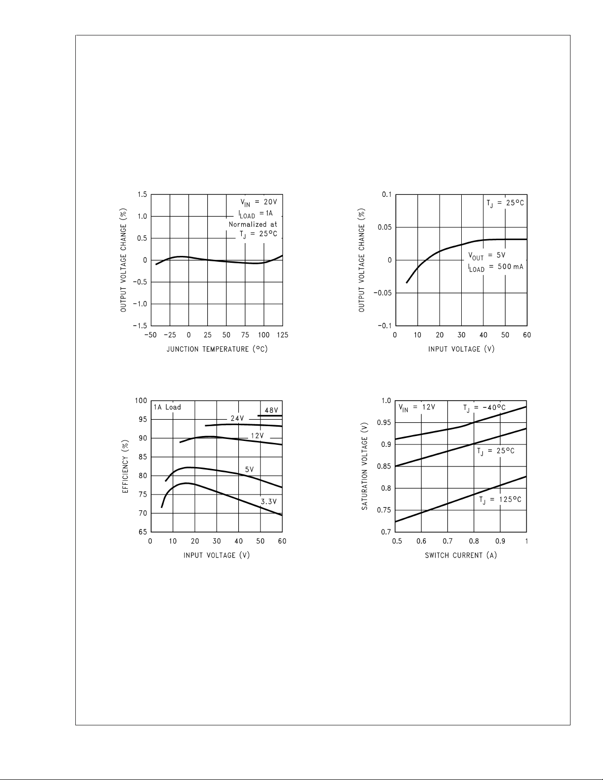
Typical Performance Characteristics (Circuit of Figure 1)
Normalized
Output Voltage Line Regulation
Efficiency
10129302
10129304
10129303
Switch Saturation
Voltage
10129305
www.national.com 4
Page 5
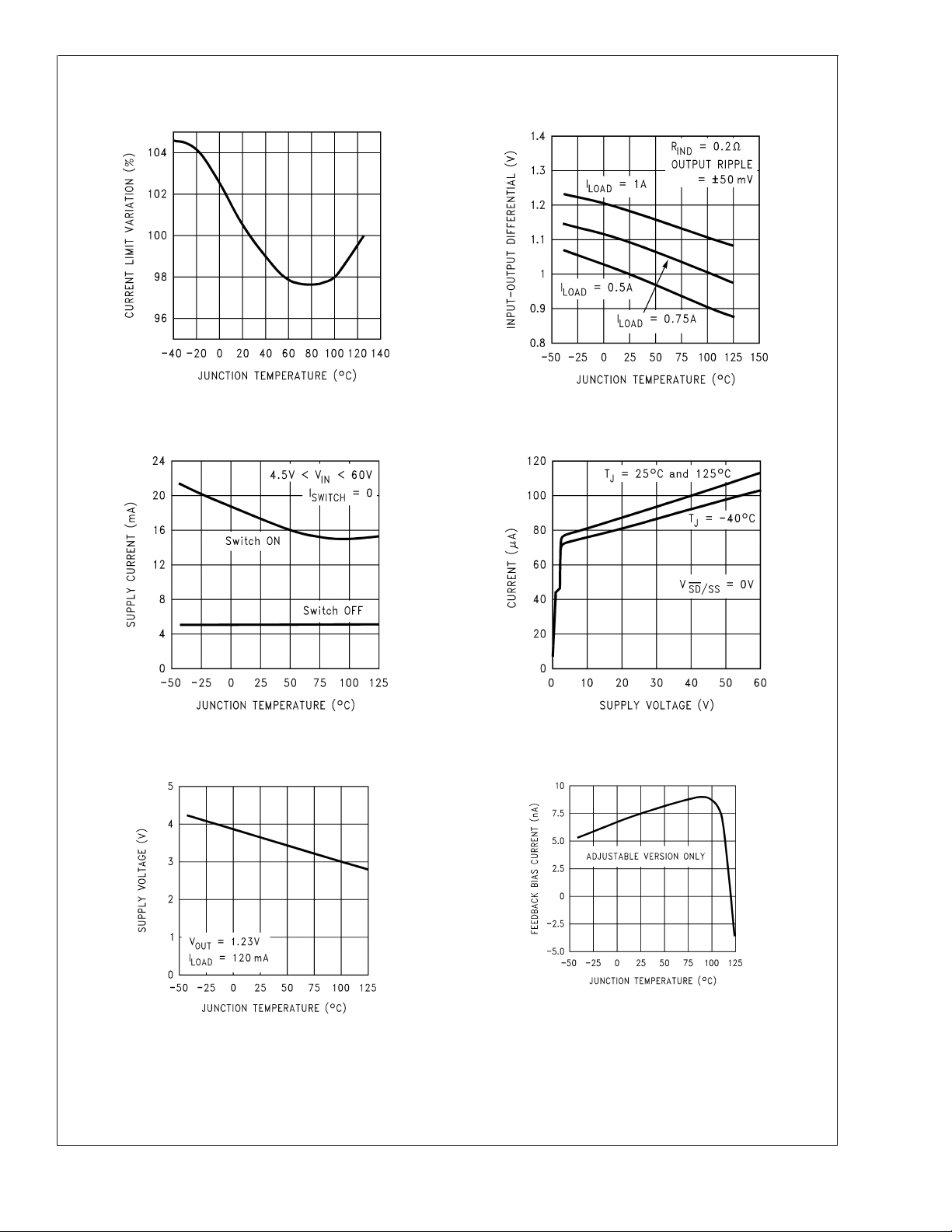
Typical Performance Characteristics (Circuit of Figure 1) (Continued)
Switch Current Limit Dropout Voltage
LM2591HV
Operating
Quiescent Current
Minimum Operating
Supply Voltage
10129306
10129307
Shutdown
Quiescent Current
10129308 10129309
Feedback Pin
Bias Current
10129310
10129311
www.national.com5
Page 6
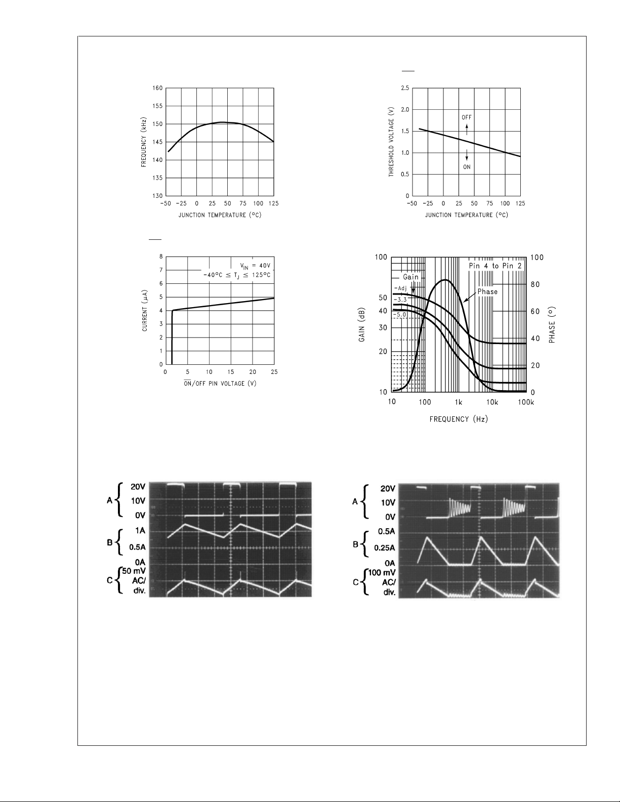
Typical Performance Characteristics (Circuit of Figure 1) (Continued)
LM2591HV
Switching Frequency ON/OFF Threshold Voltage
10129313
10129379
ON/OFF Pin Current (Sinking) Internal Gain-Phase Characteristics
Continuous Mode Switching Waveforms
= 20V, V
V
L = 52 µH, C
IN
A: Output Pin Voltage, 10V/div.
B: Inductor Current 0.5A/div.
C: Output Ripple Voltage, 50 mV/div.
= 100 µF, C
OUT
OUT
Horizontal Time Base: 2 µs/div.
= 5V, I
10129380
=1A
LOAD
ESR = 100 mΩ
OUT
10129320
Discontinuous Mode Switching Waveforms
V
= 20V, V
IN
L = 15 µH, C
A: Output Pin Voltage, 10V/div.
B: Inductor Current 0.25A/div.
C: Output Ripple Voltage, 100 mV/div.
OUT
= 5V, I
OUT
= 150 µF, C
LOAD
OUT
Horizontal Time Base: 2 µs/div.
10129378
= 250 mA
ESR=90mΩ
10129319
www.national.com 6
Page 7

Typical Performance Characteristics (Circuit of Figure 1) (Continued)
LM2591HV
Load Transient Response for Continuous Mode
V
= 20V, V
IN
L = 52 µH, C
A: Output Voltage, 100 mV/div. (AC)
B: 250 mA to 1A Load Pulse
OUT
= 100 µF, C
OUT
= 5V, I
= 250 mA to 1A
LOAD
ESR = 100 mΩ
OUT
10129321
Load Transient Response for Discontinuous Mode
V
L = 15 µH, C
A: Output Voltage, 100 mV/div. (AC)
B: 250 mA to 1A Load Pulse
Horizontal Time Base: 50 µs/div.
Connection Diagrams and Order Information
Bent and Staggered Leads, Through Hole Package
5-Lead TO-220 (T)
= 20V, V
IN
= 5V, I
OUT
= 150 µF, C
OUT
= 250 mA to 1A
LOAD
OUT
Horizontal Time Base: 200 µs/div.
Surface Mount Package
5-Lead TO-263 (S)
ESR=90mΩ
10129322
Order Number LM2591HVT-3.3, LM2591HVT-5.0,
10129381
or LM2591HVT-ADJ
See NS Package Number T05D
Order Number LM2591HVS-3.3, LM2591HVS-5.0,
10129382
or LM2591HVS-ADJ
See NS Package Number TS5B
www.national.com7
Page 8

Test Circuit and Layout Guidelines
LM2591HV
Fixed Output Voltage Versions
Component Values shown are for VIN= 15V,
10129324
= 5V, I
V
OUT
— 470 µF, 50V, Aluminum Electrolytic Nichicon “PM Series”
C
IN
— 220 µF, 25V Aluminum Electrolytic, Nichicon “PM Series”
C
OUT
LOAD
= 1A.
D1 — 2A, 60V Schottky Rectifier, 21DQ06 (International Rectifier)
L1 — 68 µH, See Inductor Selection Procedure
Adjustable Output Voltage Versions
Select R1to be approximately 1 kΩ, use a 1% resistor for best stability.
Component Values shown are for V
= 10V, I
V
OUT
: — 470 µF, 35V, Aluminum Electrolytic Nichicon “PM Series”
C
IN
: — 220 µF, 35V Aluminum Electrolytic, Nichicon “PM Series”
C
OUT
LOAD
= 1A.
IN
= 20V,
D1 — 2A, 60V Schottky Rectifier, 21DQ06 (International Rectifier)
L1 — 100 µH, See Inductor Selection Procedure
—1kΩ,1%
R
1
— 7.15k, 1%
R
2
— 3.3 nF
C
FF
Typical Values
— 0.1 µF
C
SS
— 0.1 µF
C
DELAY
R
†
— 4.7k (use 22k if V
PULL UP
Small signal Schottky diode to prevent damage to feedback pin by negative spike when output is shorted (CFFnot being able to discharge immediately will
drag feedback pin below ground). Required if V
OUT
is ≥ 45V)
>
40V
IN
10129325
FIGURE 1. Standard Test Circuits and Layout Guides
www.national.com 8
Page 9

Block Diagram
LM2591HV
10129383
Pin Functions
+VIN(Pin 1) —This is the positive input supply for the IC
switching regulator. A suitable input bypass capacitor must
be present at this pin to minimize voltage transients and to
supply the switching currents needed by the regulator.
Output (Pin 2) — Internal switch. The voltage at this pin
switches between approximately (+V
mately −0.5V, with a duty cycle of V
Ground (Pin 3)— Circuit ground.
Feedback (Pin 4) —Senses the regulated output voltage to
complete the feedback loop. This pin is directly connected to
the Output for the fixed voltage versions, but is set to 1.23V
by means of a resistive divider from the output for the
Adjustable version. If a feedforward capacitor is used (Adjustable version), then a negative voltage spike is generated
IN−VSAT
OUT/VIN
) and approxi-
.
on this pin whenever the output is shorted. This happens
because the feedforward capacitor cannot discharge fast
enough, and since one end of it is dragged to Ground, the
other end goes momentarily negative. To prevent the energy
rating of this pin from being exceeded, a small-signal Schottky diode to Ground is recommended for DC input voltages
above 40V whenever a feedforward capacitor is present
(See Figure 1). Feedforward capacitor values larger than 0.1
µF are not recommended for the same reason, whatever be
the DC input voltage.
ON /OFF (Pin 5) — The regulator is in shutdown mode,
drawing about 90 µA, when this pin is driven to a high level
(≥ 2.0V), and is in normal operation when this Pin is left
floating or driven to a low level (≤ 0.6V). The typical value of
the threshold is 1.3V and the voltage on this pin must not
exceed 25V.
www.national.com9
Page 10

Inductor Value Selection Guides
(For Continuous Mode Operation)
LM2591HV
FIGURE 2. LM2591HV-3.3
10129365
FIGURE 3. LM2591HV-5.0
www.national.com 10
10129366
Page 11

Inductor Value Selection Guides (For Continuous Mode Operation) (Continued)
LM2591HV
FIGURE 4. LM2591HV-ADJ
FIGURE 5. Current Ripple Ratio
10129367
10129368
www.national.com11
Page 12

Inductor Value Selection Guides (For Continuous Mode Operation) (Continued)
LM2591HV
Coilcraft Inc. Phone (USA): 1-800-322-2645
Web Address http://www.coilcraft.com
Coilcraft Inc., Europe Phone (UK): 1-236-730595
Web Address http://www.coilcraft-europe.com
Pulse Engineering Inc. Phone (USA): 1-858-674-8100
Web Address http://www.pulseeng.com
Pulse Engineering Inc., Phone (UK): 1-483-401700
Europe Web Address http://www.pulseeng.com
Renco Electronics Inc. Phone (USA): 1-321-637-1000
Web Address http://www.rencousa.com
Schott Corp. Phone (USA): 1-952-475-1173
Web Address http://www.shottcorp.com
Cooper Electronic Tech.
(Coiltronics)
TDK Phone (USA): 1-847-803-6100
FIGURE 6. Contact Information for Suggested Inductor Manufacturers
Phone (USA): 1-888-414-2645
Web Address http://www.cooperet.com
Web Address http://www.componet.tdk.com
www.national.com 12
Page 13

Application Information
INDUCTOR SELECTION PROCEDURE
Application Note AN-1197 titled "Selecting Inductors for Buck
Converters" provides detailed information on this topic. For a
quick-start the designer may refer to the nomographs provided in Figure 2 to Figure 4. To widen the choice of the
Designer to a more general selection of available inductors,
the nomographs provide the required inductance and also
the energy in the core expressed in microjoules (µJ), as an
alternative to just prescribing custom parts. The following
points need to be highlighted:
1. The Energy values shown on the nomographs apply to
steady operation at the corresponding x-coordinate
(rated maximum load current). However under start-up,
without soft-start, or a short-circuit on the output, the
current in the inductor will momentarily/repetitively hit
the current limit I
could be much higher than the rated load, I
represents an overload situation, and can cause the
Inductor to saturate (if it has been designed only to
handle the energy of steady operation). However most
types of core structures used for such applications have
a large inherent air gap (for example powdered iron
types or ferrite rod inductors), and so the inductance
does not fall off too sharply under an overload. The
device is usually able to protect itself by not allowing the
current to ever exceed I
to the regulator is over 40V, the current can slew up so
fast under core saturation, that the device may not be
able to act fast enough to restrict the current. The current can then rise without limit till destruction of the
device takes place. Therefore to ensure reliability, it is
recommended, that if the DC Input Voltage exceeds
40V, the inductor must ALWAYS be sized to handle an
instantaneous current equal to I
irrespective of the type of core structure/material.
2. The Energy under steady operation is
of the device, and this current
CLIM
. But if the DC input voltage
CLIM
without saturating,
CLIM
LOAD
. This
consider the rather wide tolerance on the nominal inductance of commercial inductors.
5. Figure 4 shows the inductor selection curves for the
Adjustable version. The y-axis is ’Et’, in Vµsecs. It is the
applied volts across the inductor during the ON time of
the switch (V
IN-VSAT-VOUT
) multiplied by the time for
which the switch is on in µsecs. See Example 3 below.
Example 1: (V
@
0.8A
5V
≤ 40V) LM2591HV-5.0, VIN= 24V, Output
IN
1. A first pass inductor selection is based upon Inductance
and rated max load current. We choose an inductor with the
Inductance value indicated by the nomograph (Figure 3) and
a current rating equal to the maximum load current. We
therefore quick-select a 100µH/0.8A inductor (designed for
150 kHz operation) for this application.
2. We should confirm that it is rated to handle 50 µJ (see
Figure 3) by either estimating the peak current or by a
detailed calculation as shown in AN-1197, and also that the
losses are acceptable.
>
Example 2: (V
@
1A
5V
40V) LM2591HV-5.0, VIN= 48V, Output
IN
1. A first pass inductor selection is based upon Inductance
and the switch currrent limit. We choose an inductor with the
Inductance value indicated by the nomograph (Figure 3) and
a current rating equal to I
. We therefore quick-select a
CLIM
100µH/3A inductor (designed for 150 kHz operation) for this
application.
2. We should confirm that it is rated to handle e
CLIM
by the
procedure shown in AN-1197 and that the losses are acceptable. Here e
CLIM
is:
LM2591HV
where L is in µH and I
current waveform with the regulator delivering I
is the peak of the inductor
PEAK
LOAD
These are the energy values shown in the nomographs.
See Example 1 below.
3. The Energy under overload is
>
If V
e
CLIM
case I
40V, the inductor should be sized to handle
IN
instead of the steady energy values. The worst
for the LM2591HV is 3A. The Energy rating
CLIM
depends on the Inductance. See Example 2 below.
4. The nomographs were generated by allowing a greater
amount of percentage current ripple in the Inductor as
the maximum rated load decreases (see Figure 5). This
was done to permit the use of smaller inductors at light
loads. Figure 5 however shows only the ’median’ value
of the current ripple. In reality there may be a great
spread around this because the nomographs approximate the exact calculated inductance to standard available values. It is a good idea to refer to AN-1197 for
detailed calculations if a certain maximum inductor current ripple is required for various possible reasons. Also
Example 3: (VIN≤ 40V) LM2591HV-ADJ, VIN= 20V, Output
@
1A
10V
1. Since input voltage is less than 40V, a first pass inductor
selection is based upon Inductance and rated max load
.
current. We choose an inductor with the Inductance value
indicated by the nomograph Figure 4 and a current rating
equal to the maximum load. But we first need to calculate Et
for the given application. The Duty cycle is
where VDis the drop across the Catch Diode () 0.5V for a
Schottky) and V
the drop across the switch ()1.5V). So
SAT
And the switch ON time is
where f is the switching frequency in Hz. So
www.national.com13
Page 14

Application Information (Continued)
LM2591HV
Therefore, looking at Figure 2 we quick-select a 100µH/1A
inductor (designed for 150 kHz operation) for this application.
2. We should confirm that it is rated to handle 100 µJ (see
Figure 4) by the procedure shown in AN-1197 and that the
losses are acceptable. (If the DC Input voltage had been
greater than 40V we would need to consider e
Example 2 above).
Note that we have taken V
estimated resistive drop across the inductor.
This completes the simplified inductor selection procedure.
For more general applications and better optimization, the
designer should refer to AN-1197. Figure 6 provides helpful
contact information on suggested Inductor manufacturers
who may be able to recommend suitable parts, if the requirements are known.
FEEDFORWARD CAPACITOR
(Adjustable Output Voltage Version)
- A Feedforward Capacitor CFF, shown across R2 in
C
FF
Figure 1 is used when the output voltage is greater than 10V
or when C
has a very low ESR. This capacitor adds lead
OUT
compensation to the feedback loop and increases the phase
margin for better loop stability.
If the output voltage ripple is large (
output voltage), this ripple can be coupled to the feedback
pin through the feedforward capacitor and cause the error
comparator to trigger the error flag. In this situation, adding a
resistor, R
, in series with the feedforward capacitor, ap-
FF
proximately 3 times R1, will attenuate the ripple voltage at
the feedback pin.
INPUT CAPACITOR
C
— A low ESR aluminum or tantalum bypass capacitor is
IN
needed between the input pin and ground pin. It must be
located near the regulator using short leads. This capacitor
prevents large voltage transients from appearing at the input, and provides the instantaneous current needed each
time the switch turns on.
The important parameters for the Input capacitor are the
voltage rating and the RMS current rating. Because of the
relatively high RMS currents flowing in a buck regulator’s
input capacitor, this capacitor should be chosen for its RMS
current rating rather than its capacitance or voltage ratings,
although the capacitance value and voltage rating are directly related to the RMS current rating. The voltage rating of
the capacitor and its RMS ripple current capability must
never be exceeded.
as 1.5V which includes an
SAT
>
5% of the nominal
CLIM
as in
OUTPUT CAPACITOR
— An output capacitor is required to filter the output
C
OUT
and provide regulator loop stability. Low impedance or low
ESR Electrolytic or solid tantalum capacitors designed for
switching regulator applications must be used. When selecting an output capacitor, the important capacitor parameters
are; the 100 kHz Equivalent Series Resistance (ESR), the
RMS ripple current rating, voltage rating, and capacitance
value. For the output capacitor, the ESR value is the most
important parameter. The ESR should generally not be less
than 100 mΩ or there will be loop instability. If the ESR is too
large, efficiency and output voltage ripple are effected. So
ESR must be chosen carefully.
CATCH DIODE
Buck regulators require a diode to provide a return path for
the inductor current when the switch turns off. This must be
a fast diode and must be located close to the LM2591HV
using short leads and short printed circuit traces.
Because of their very fast switching speed and low forward
voltage drop, Schottky diodes provide the best performance,
especially in low output voltage applications (5V and lower).
Ultra-fast recovery, or High-Efficiency rectifiers are also a
good choice, but some types with an abrupt turnoff characteristic may cause instability or EMI problems. Ultra-fast
recovery diodes typically have reverse recovery times of 50
ns or less. The diode must be chosen for its average/RMS
current rating and maximum voltage rating. The voltage
rating of the diode must be greater than the DC input voltage
(not the output voltage).
DELAYED STARTUP
The circuit in Figure 7 uses the the ON /OFF pin to provide
a time delay between the time the input voltage is applied
and the time the output voltage comes up (only the circuitry
pertaining to the delayed start up is shown). As the input
voltage rises, the charging of capacitor C1 pulls the ON /OFF
pin high, keeping the regulator off. Once the input voltage
reaches its final value and the capacitor stops charging, and
resistor R
pulls the ON /OFF pin low, thus allowing the
2
circuit to start switching. Resistor R1is included to limit the
maximum voltage applied to the ON /OFF pin (maximum of
25V), reduces power supply noise sensitivity, and also limits
the capacitor, C1, discharge current. When high input ripple
voltage exists, avoid long delay time, because this ripple can
be coupled into the ON /OFF pin and cause problems.
This delayed startup feature is useful in situations where the
input power source is limited in the amount of current it can
deliver. It allows the input voltage to rise to a higher voltage
before the regulator starts operating. Buck regulators require
less input current at higher input voltages.
www.national.com 14
Page 15

Application Information (Continued)
FIGURE 7. Delayed Startup
LM2591HV
10129336
UNDERVOLTAGE LOCKOUT
Some applications require the regulator to remain off until
the input voltage reaches a predetermined voltage. An undervoltage lockout feature applied to a buck regulator is
shown in Figure 8, while Figure 9 and Figure 10 applies the
same feature to an inverting circuit. The circuit in Figure 9
features a constant threshold voltage for turn on and turn off
(zener voltage plus approximately one volt). If hysteresis is
FIGURE 8. Undervoltage Lockout for Buck Regulator
needed, the circuit in Figure 10 has a turn ON voltage which
is different than the turn OFF voltage. The amount of hysteresis is approximately equal to the value of the output voltage. If zener voltages greater than 25V are used, an additional 47 kΩ resistor is needed from the ON /OFF pin to the
ground pin to stay within the 25V maximum limit of the ON
/OFF pin.
10129337
www.national.com15
Page 16

Application Information (Continued)
LM2591HV
This circuit has an ON/OFF threshold of approximately 13V.
FIGURE 9. Undervoltage Lockout for Inverting Regulator
10129384
lNVERTING REGULATOR
The circuit in Figure 11 converts a positive input voltage to a
negative output voltage with a common ground. The circuit
operates by bootstrapping the regulator’s ground pin to the
negative output voltage, then grounding the feedback pin,
the regulator senses the inverted output voltage and regulates it.
This example uses the LM2591HV-5.0 to generate a −5V
output, but other output voltages are possible by selecting
other output voltage versions, including the adjustable version. Since this regulator topology can produce an output
voltage that is either greater than or less than the input
voltage, the maximum output current greatly depends on
both the input and output voltage.
To determine how much load current is possible before the
internal device current limit is reached (and power limiting
occurs), the system must be evaluated as a buck-boost
configuration rather than as a buck. The peak switch current
in Amperes, for such a configuration is given as:
where L is in µH and f is in Hz. The maximum possible load
current I
is limited by the requirement that I
LOAD
While checking for this, take I
to be the lowest possible
CLIM
PEAK
≤ I
CLIM
current limit value (min across tolerance and temperature is
1.2A for the LM2591HV). Also to account for inductor toler-
ances, we should take the min value of Inductance for L in
the equation above (typically 20% less than the nominal
value). Further, the above equation disregards the drop
across the Switch and the diode. This is equivalent to assuming 100% efficiency, which is never so. Therefore expect
to be an additional 10-20% higher than calculated from
I
PEAK
the above equation.
The reader is also referred to Application Note AN-1157 for
examples based on positive to negative configuration.
The maximum voltage appearing across the regulator is the
absolute sum of the input and output voltage, and this must
be limited to a maximum of 60V. For example, when converting +20V to −12V, the regulator would see 32V between the
input pin and ground pin. The LM2591HV has a maximum
input voltage spec of 60V.
Additional diodes are required in this regulator configuration.
Diode D1 is used to isolate input voltage ripple or noise from
coupling through the C
capacitor to the output, under light
IN
or no load conditions. Also, this diode isolation changes the
topology to closley resemble a buck configuration thus providing good closed loop stability. A Schottky diode is recommended for low input voltages, (because of its lower voltage
drop) but for higher input voltages, a fast recovery diode
could be used.
.
Without diode D3, when the input voltage is first applied, the
charging current of C
can pull the output positive by sev-
IN
eral volts for a short period of time. Adding D3 prevents the
output from going positive by more than a diode voltage.
www.national.com 16
Page 17

Application Information (Continued)
This circuit has hysteresis
Regulator starts switching at V
Regulator stops switching at V
FIGURE 10. Undervoltage Lockout with Hysteresis for Inverting Regulator
= 13V
IN
=8V
IN
LM2591HV
10129339
CIN— 68 µF/25V Tant. Sprague 595D
470 µF/50V Elec. Panasonic HFQ
— 47 µF/20V Tant. Sprague 595D
C
OUT
220 µF/25V Elec. Panasonic HFQ
FIGURE 11. Inverting −5V Regulator with Delayed Startup
Because of differences in the operation of the inverting
regulator, the standard design procedure is not used to
select the inductor value. In the majority of designs, a 33 µH,
3A inductor is the best choice. Capacitor selection can also
be narrowed down to just a few values.
This type of inverting regulator can require relatively large
amounts of input current when starting up, even with light
loads. Input currents as high as the LM2591HV current limit
(approx 4A) are needed for at least 2 ms or more, until the
output reaches its nominal output voltage. The actual time
depends on the output voltage and the size of the output
capacitor. Input power sources that are current limited or
sources that can not deliver these currents without getting
loaded down, may not work correctly. Because of the relatively high startup currents required by the inverting topology,
the delayed startup feature (C1, R
and R2) shown in Figure
1
10129340
11 is recommended. By delaying the regulator startup, the
input capacitor is allowed to charge up to a higher voltage
before the switcher begins operating. A portion of the high
input current needed for startup is now supplied by the input
capacitor (C
). For severe start up conditions, the input
IN
capacitor can be made much larger than normal.
lNVERTING REGULATOR SHUTDOWN METHODS
To use the ON /OFF pin in a standard buck configuration is
simple, pull it below 1.3V (@25˚C, referenced to ground) to
turn regulator ON, pull it above 1.3V to shut the regulator
OFF. With the inverting configuration, some level shifting is
required, because the ground pin of the regulator is no
longer at ground, but is now setting at the negative output
voltage level. Two different shutdown methods for inverting
regulators are shown in Figure 12 and Figure 13
www.national.com17
Page 18

Application Information (Continued)
LM2591HV
FIGURE 12. Inverting Regulator Ground Referenced Shutdown
10129342
FIGURE 13. Inverting Regulator Ground Referenced Shutdown using Opto Device
LAYOUT SUGGESTIONS
As in any switching regulator, layout is very important. Rapidly switching currents associated with wiring inductance can
generate voltage transients which can cause problems. For
minimal inductance and ground loops, with reference to
Figure 1, the wires indicated by heavy lines should be wide
printed circuit traces and should be kept as short as
possible. For best results, external components should be
located as close to the switcher lC as possible using ground
plane construction or single point grounding.
10129386
If open core inductors are used, special care must be
taken as to the location and positioning of this type of inductor. Allowing the inductor flux to intersect sensitive feedback,
lC groundpath and C
wiring can cause problems.
OUT
When using the adjustable version, special care must be
taken as to the location of the feedback resistors and the
associated wiring. Physically locate both resistors near the
IC, and route the wiring away from the inductor, especially an
open core type of inductor.
www.national.com 18
Page 19

Physical Dimensions inches (millimeters)
unless otherwise noted
LM2591HV
5-Lead TO-220 Bent and Staggered Package
Order Number LM2591HVT-3.3, LM2591HVT-5.0
or LM2591HVT-ADJ
NS Package Number T05D
www.national.com19
Page 20

Physical Dimensions inches (millimeters) unless otherwise noted (Continued)
5-Lead TO-263 Bent and Formed Package
Order Number LM2591HVS-3.3, LM2591HVS-5.0 or LM2591HVS-ADJ
NS Package Number TS5B
LIFE SUPPORT POLICY
NATIONAL’S PRODUCTS ARE NOT AUTHORIZED FOR USE AS CRITICAL COMPONENTS IN LIFE SUPPORT
DEVICES OR SYSTEMS WITHOUT THE EXPRESS WRITTEN APPROVAL OF THE PRESIDENT AND GENERAL
COUNSEL OF NATIONAL SEMICONDUCTOR CORPORATION. As used herein:
1. Life support devices or systems are devices or
systems which, (a) are intended for surgical implant
into the body, or (b) support or sustain life, and
whose failure to perform when properly used in
accordance with instructions for use provided in the
2. A critical component is any component of a life
support device or system whose failure to perform
can be reasonably expected to cause the failure of
the life support device or system, or to affect its
safety or effectiveness.
labeling, can be reasonably expected to result in a
significant injury to the user.
LM2591HV SIMPLE SWITCHER Power Converter 150 kHz 1A Step-Down Voltage Regulator
National Semiconductor
Americas Customer
Support Center
Email: new.feedback@nsc.com
Tel: 1-800-272-9959
www.national.com
National Semiconductor
Europe Customer Support Center
Fax: +49 (0) 180-530 85 86
Email: europe.support@nsc.com
Deutsch Tel: +49 (0) 69 9508 6208
English Tel: +44 (0) 870 24 0 2171
Français Tel: +33 (0) 1 41 91 8790
National Semiconductor
Asia Pacific Customer
Support Center
Email: ap.support@nsc.com
National Semiconductor
Japan Customer Support Center
Fax: 81-3-5639-7507
Email: jpn.feedback@nsc.com
Tel: 81-3-5639-7560
National does not assume any responsibility for use of any circuitry described, no circuit patent licenses are implied and National reserves the right at any time without notice to change said circuitry and specifications.
 Loading...