

Datasheet LM2576BT, LM2576-5.0BU, LM2576-5.0BT, LM2576-3.3BU, LM2576-12BU Datasheet (MICREL)
...Page 1
LM2576 Micrel
LM2576
52kHz Simple 3A Buck Voltage Regulator
General Description
The LM2576 series of monolithic integrated circuits provide
all the active functions for a step-down (buck) switching
regulator. Fixed versions are available with a 3.3V, 5V, or 12V
fixed output. Adjustable versions have an output voltage
range from 1.23V to 37V. Both versions are capable of driving
a 3A load with excellent line and load regulation.
These regulators are simple to use because they require a
minimum number of external components and include internal
frequency compensation and a fixed-frequency oscillator.
The LM2576 series offers a high efficiency replacement for
popular three-terminal adjustable linear regulators. It
substantially reduces the size of the heat sink, and in many
cases no heat sink is required.
A standard series of inductors available from several different
manufacturers are ideal for use with the LM2576 series. This
feature greatly simplifies the design of switch-mode power
supplies.
The feedback voltage is guaranteed to ±2% tolerance for
adjustable versions, and the output voltage is guaranteed to
±3% for fixed versions, within specified input voltages and
output load conditions. The oscillator frequency is guaranteed
to ±10%. External shutdown is included, featuring less than
200µA standby current. The output switch includes cycle-bycycle current limiting and thermal shutdown for full protection
under fault conditions.
Features
• 3.3V, 5V, 12V, and adjustable output versions
• Voltage over specified line and load conditions:
Fixed version: ±3% max. output voltage
Adjustable version: ±2% max. feedback voltage
• Guaranteed 3A output current
• Wide input voltage range:
4V to 40V
• Wide output voltage range
1.23V to 37V
• Requires only 4 external components
• 52kHz fixed frequency internal oscillator
• Low power standby mode IQ typically < 200µA
• 80% efficiency (adjustable version typically > 80%)
• Uses readily available standard inductors
• Thermal shutdown and current limit protection
• 100% electrical thermal limit burn-in
Applications
• Simple high-efficiency step-down (buck) regulator
• Efficient pre-regulator for linear regulators
• On-card switching regulators
• Positive to negative converter (inverting Buck-Boost)
• Isolated Flyback Converter using minimum number of
external components
• Negative Boost Converter
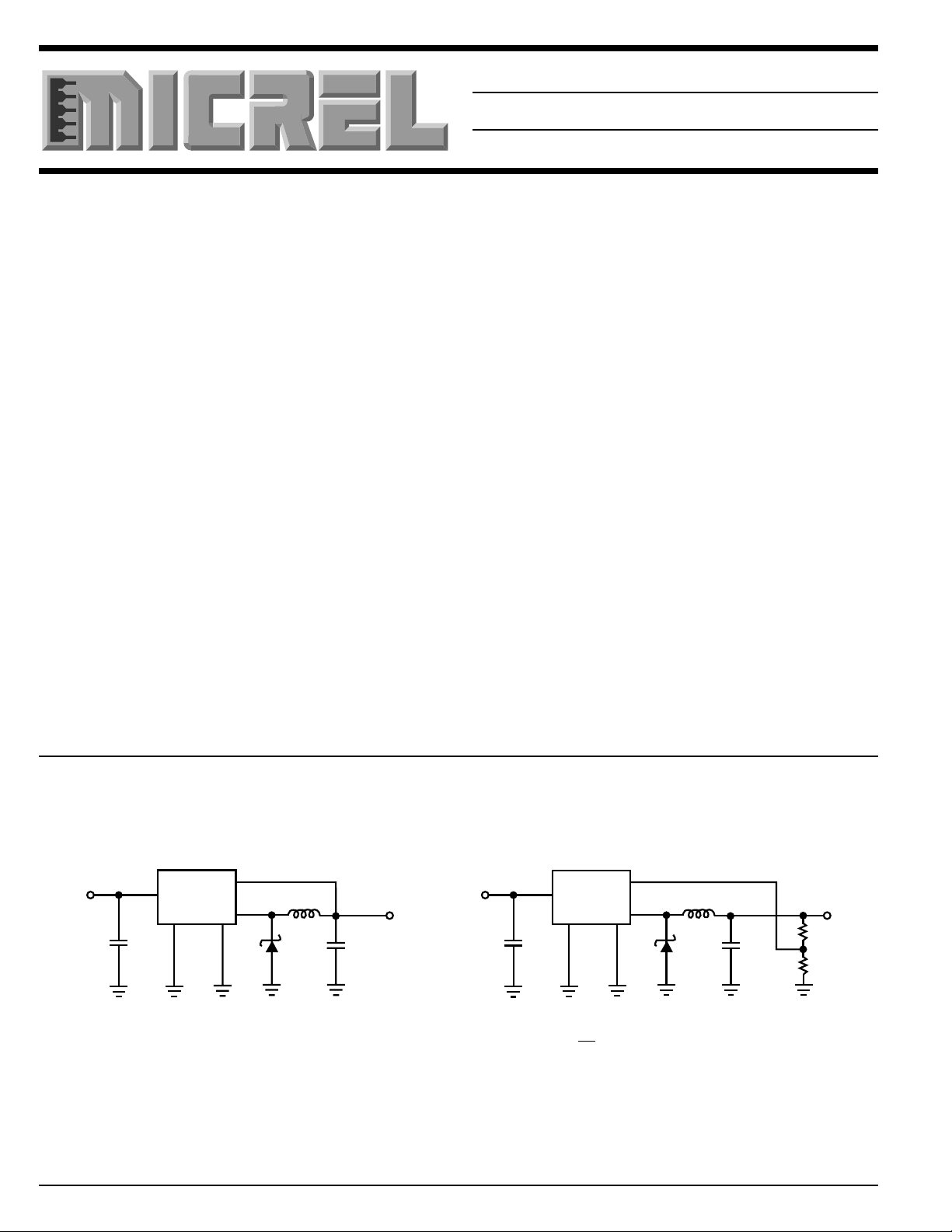
Typical Applications
7V–40V
Unregulated
DC Input
C
IN
100µF
Note: Pin numbers are for TO-220 Package
+V
+
1
LM2576-5.0
IN
3
Gnd5On/Off
Fixed Regulator in Typical Application Adjustable Regulator in Fixed Output Application
4
Output
2
Feedback
L1
100µH
D1
1N5822
+5V, 3A
Regulated
Output
+
C
OUT
1000µF
7V–40V
Unregulated
DC Input
C
IN
100µF
Note: Pin numbers are for TO-220 Package
V
OUT
1
+V
IN
+
= 1.23 1 +
3
Gnd5On/Off
( )
LM2576
R2
R1
4
Output
2
Feedback
L1
100µH
D1
1N5822
+
C
OUT
1000µF
Regulated
870 20
+5V, 3A
Output
R2 3.09k
R1 1k
4-120 October 1998
Page 2
LM2576 Micrel
Ordering Information
Part Number
LM2576BT*
LM2576-3.3BT
LM2576-5.0BT
LM2576-12BT
‡
Temperature Range Package
†
†
†
†
–40°C to +85°C 5-lead TO-220
–40°C to +85°C 5-lead TO-220
–40°C to +85°C 5-lead TO-220
–40°C to +85°C 5-lead TO-220
LM2576BU* –40°C to +85°C 5-lead TO-263
LM2576-3.3BU –40°C to +85°C 5-lead TO-263
LM2576-5.0BU –40°C to +85°C 5-lead TO-263
LM2576-12BU –40°C to +85°C 5-lead TO-263
* Adjustable output regulators.
†
Contact factory for bent or staggered leads option.
4
Pin Configurations
5-LEAD TO-220 (T)
GND
5- ON/OFF
4- FEEDBACK
3- GROUND
2- OUTPUT
1- V
IN
5-LEAD TO-263 (U)
GND
5- ON/OFF
4- FEEDBACK
3- GROUND
2- OUTPUT
1- V
IN
October 1998 4-121
Page 3
LM2576 Micrel
Absolute Maximum Ratings (Note 1)
Maximum Supply Voltage 45V
ON/OFF Pin Input Voltage –0.3V ≤ V ≤ +40V
Operating Ratings
Temperature Range –40°C ≤ TJ ≤ +125°C
Supply Voltage 40V
Output Voltage to Ground (Steady State) –1V
Power Dissipation Internally Limited
Storage Temperature Range –65°C to +150°C
Minimum ESD Rating
C = 100pF, R = 1.5kΩ 2 kV
FB Pin 1 kV
Lead Temperature (soldering, 10 sec.) 260°C
Maximum Junction Temperature 150°C
Electrical Characteristics Specifications with standard typeface are for T
over full Operating Temperature Range. Unless otherwise specified, V
= 12V, and I
IN
= 25°C, and those with boldface type apply
J
= 500mA.
LOAD
LM2576
Symbol Parameter Conditions Typ Limit Units
(Note 2) (Limits)
SYSTEM PARAMETERS, ADJUSTABLE REGULATORS (Note 3) Test Circuit
V
OUT
V
OUT
η Efficiency VIN = 12V, I
SYSTEM PARAMETERS, 3.3V REGULATORS (Note 3) Test Circuit
V
OUT
V
OUT
η Efficiency VIN = 12V, I
SYSTEM PARAMETERS, 5V REGULATORS (Note 3) Test Circuit
V
OUT
V
OUT
η Efficiency VIN = 12V, I
SYSTEM PARAMETERS, 12V REGULATORS (Note 3) Test Circuit
V
OUT
V
OUT
η Efficiency VIN = 25V, I
Feedback Voltage VIN = 12V , I
V
= 5V 1.217 V(min)
OUT
Feedback Voltage 0.5A ≤ I
LM2576 V
LOAD
= 5V 1.193/1.180 V(min)
OUT
Output Voltage VIN = 12V , I
V
= 3.3V 3.234 V(min)
OUT
Output Voltage 0.5A ≤ I
LM2576-3.3 V
LOAD
= 3.3V 3.168/3.135 V(min)
OUT
Output Voltage VIN = 12V , I
V
= 5V 4.900 V(min)
OUT
Output Voltage 0.5A ≤ I
LM2576-5.0 V
LOAD
= 5V 4.800/4.750 V(min)
OUT
Output Voltage VIN = 25V , I
V
= 12V 11.760 V(min)
OUT
Output Voltage 0.5A ≤ I
LMLM2576-12 V
LOAD
= 12V 11.520/11.400 V(min)
OUT
= 0.5A 1.230 V
LOAD
≤ 3A, 6V ≤ VIN ≤ 40V 1.230 V
LOAD
= 3A, V
= 5V 82 %
OUT
Figure 1
= 0.5A 3.3 V
LOAD
≤ 3A, 6V ≤ VIN ≤ 40V 3.3 V
= 3A 75 %
LOAD
Figure 1
= 0.5A 5.0 V
LOAD
≤ 3A, 8V ≤ VIN ≤ 40V 5.0 V
= 3A 82 %
LOAD
Figure 1
= 0.5A 12 V
LOAD
≤ 3A, 15V ≤ VIN ≤ 40V 12 V
= 3A 88 %
LOAD
Figure 1
1.243 V(max)
1.267/1.280 V(max)
3.366 V(max)
3.432/3.465 V(max)
5.100 V(max)
5.200/5.250 V(max)
12.240 V(max)
12.480/12.600 V(max)
4-122 October 1998
Page 4

LM2576 Micrel
Electrical Characteristics (continued)
LM2576 Units
Symbol Parameter Conditions Typ Limit (Limits)
(Note 2)
DEVICE PARAMETERS, ADJUSTABLE REGULATOR
I
B
DEVICE PARAMETERS, FIXED and ADJUSTABLE REGULATORS
f
O
V
SAT
DC Max Duty Cycle (ON) (Note 5) 98 %
I
CL
I
L
I
Q
I
STBY
θ
JA
θ
JA
θ
JC
Feedback Bias Current V
= 5V 50 100/500 nA
OUT
Oscillator Frequency 52 kHz
47/42 kHz (min)
58/63 kHz (max)
Saturation Voltage I
= 3A (Note 4) 1.4 V
OUT
1.8/2.0 V(max)
93 %(min)
Current Limit Peak Current, t
≤ 3µs (Note 4) 5.8 A
ON
4.2/3.5 A(min)
6.9/7.5 A(max)
Output Leakage Current VIN = 40V, (Note 6), Output = 0V 2 mA(max)
Output = –1V 7.5 mA
(Note 6) Output = –1V 30 mA(max)
Quiescent Current (Note 6) 5 mA
10 mA(max)
Standby Quiescent ON/OFF Pin = 5V (OFF) 50 µA
Current 200 µA(max)
Thermal Resistance T,U Package, Junction to Ambient (Note 7) 65 °C/W
T,U Package, Junction to Ambient (Note 8) 45
T,U Package, Junction to Case 2
4
October 1998 4-123
Page 5

LM2576 Micrel
Electrical Characteristics (continued)
LM2576 Units
Symbol Parameter Conditions Typ Limit (Limits)
(Note 2)
ON/OFF CONTROL, FIXED and ADJUSTABLE REGULATORS Test Circuit
V
IH
V
IL
I
IH
I
IL
Note 1: Absolute Maximum Rating indicate limits beyond which damage to the device may occur. Operating Ratings indicate conditions for which the device
Note 2: All limits guaranteed at room temperature (standard type face) and at temperature extremes (bold type face) . All room temperature limits are
Note 3: External components such as the catch diode, inductor, input and output capacitors can affect switching regulator system performance. When the
Note 4: Output (pin 2) sourcing current. No diode, inductor or capacitor connected to output.
Note 5: Feedback (pin 4) removed from output and connected to 0V.
Note 6: Feedback (pin 4) removed from output and connected to 12V to force the output transistor OFF.
Note 7: Junction to ambient thermal resistance (no external heat sink) for the 5-lead TO-220 package mounted vertically, with 1/2" leads in a socket, or
Note 8: Junction to ambient thermal resistance (no external heat sink) for the 5-lead TO-220 package mounted vertically, with 1/4" leads soldered to PC
Note 9: Junction to ambient thermal resistance with approximately 1 square inch of pc board copper surrounding the leads. Additional copper will lower
ON/OFF Pin Logic V
Input Level V
= 0V 1.4 2.2/2.4 V(min)
OUT
= 5V 1.2 1.0/0.8 V(max)
OUT
ON /OFF Pin Logic ON /OFF Pin = 5V (OFF) 4 µA
Current 30 µA(max)
ON/OFF Pin = 0V (ON) 0.01 µA
is intended to be functional, but do not guarantee specific performance limits. For guaranteed specifications and test conditions, see the Electrical
Characteristics.
100% production tested. All limits at temperature extreme are guaranteed via testing.
LM2576/LM1576 is used as shown in
Characteristics.
on PC board with minimum copper area.
board containing approximately 4 square inches of copper area surrounding the leads.
thermal resistance further.
Figure 1
test circuit, system performance will be shown in system parameters section of Electrical
Figure 1
10 µA(max)
Typical Performance Characteristics
Normalized
Feedback Voltage*
25
20
15
10
5
0
-5
-10
-15
-20
NORMALIZED FEEDBACK VOLTAGE (mV)
-25
-75 -50 -25 0 25 50 75 100125150
JUNCTION TEMPERATURE (˚C)
VIN = 12V
I
= 200mA
LOAD
Normalized to TJ = 25˚C
Feedback Voltage
vs Duty Cycle*
20
15
10
5
0
-5
-10
-15
FEEDBACK VOLTAGE CHANGE (mV)
-20
0 20 40 60 80 100
* Adjustable version only
ILOAD = 200 mA
VIN = 40V
VIN = 7V
DUTY CYCLE (%)
4-124 October 1998
Page 6

LM2576 Micrel
Typical Performance Characteristics (continued) (Circuit of
Supply Current
20
18
16
14
12
10
8
SUPPLY CURRENT (mA)
6
4
0102030405060
Measured at
Ground Pin
TJ = 25˚C
V
I
to 1A
LOAD
INPUT VOLTAGE (V)
Current Limit
6.5
6.0
5.5
5.0
OUTPUT CURRENT (A)
4.5
4.0
-75
-50 -25 0 25 50 75 100125150 0.5 1.0 1.5 2.0 2.5 3.0
JUNCTION TEMPERATURE (˚C)
= 5V
OUT
VIN = 12V
Supply Current
vs. Duty Cycle
20.0
17.5
15.0
12.5
10.0
I
7.5
5.0
SUPPLY CURRENT (mA)
2.5
0
0 2040 6080100
= 200 mA
LOAD
VIN from 7V to 40V
DUTY CYCLE (%)
Switch
Saturation Voltage
1.5
1.4
1.2
-55˚C
1.0
0.8
25˚C
0.6
150˚C
0.4
SATURATION VOLTAGE (V)
0.2
0
0
SWITCH CURRENT (A)
Figure 1
)
Standby
Quiescent Current
200
150
100
50
STANDBY QUIESCENT CURRENT (µA)
0
-75
-50 -25 0 25 50 75 100 125150
Efficiency
100
95
90
85
80
200 mA
75
EFFICIENCY (%)
70
1A
65
3A
60
0 5 10 15 20 25 30 35 40
VIN = 40V
V
= 5V
ON/OFF
VIN = 12V
JUNCTION TEMPERATURE (˚C)
V
= 12V
OUT
200 mA
V
= 3V
OUT
INPUT VOLTAGE (V)
1A
3A
4
Minimum Operating
Voltage
5.0
4.5
4.0
3.5
3.0
2.5
2.0
1.5
INPUT VOLTAGE (V)
1.0
0.5
0
-75 -50 -25 0 25 50 75 100125150
JUNCTION TEMPERATURE (˚C)
V
I
LOAD
OUT
Normalized
Output Voltage
100
75
50
25
0
-25
-50
-75
OUTPUT VOLTAGE CHANGE (mV)
-100
-75 -50 -25 0 25 50 75 100125150
JUNCTION TEMPERATURE (˚C)
VIN = 12V
I
= 200mA
LOAD
Normalized to TJ = 25˚C
= 1.23V
= 200 mA
Line Regulation
14
Normalized to VIN = 10V
12
V
= 5V
OUT
10
I
= 500mA
LOAD
8
TJ = 25
6
4
2
0
-2
-4
NORMALIZED FEEDBACK VOLTAGE (mV)
-6
0
51015202530
INPUT VOLTAGE (V)
Oscillator Frequency
+8
+6
+4
+2
0
-2
-4
--6
NORMALIZED FREQUENCY (%)
-8
-75
-50 -25 0 25 50 75 100125150
JUNCTION TEMPERATURE (˚C)
Normalized at 25˚C
VIN = 40V
VIN = 12V
Feedback Pin Current
100
75
50
25
0
-25
-50
-75
STANDBY QUIESCENT CURRENT (µA)
-100
-75
-50 -25 0 25 50 75 100 125150
JUNCTION TEMPERATURE (˚C)
Dropout Voltage
2.0
I
= 3A
LOAD
1.5
1.0
I
= 200 mA
0.5
INPUT-OUTPUT DIFFERENTIAL (V)
0
-75 -50 -25 0 25 50 75 100125150
LOAD
JUNCTION TEMPERATURE (˚C)
L1 = 330 µH
I
= 1A
LOAD
October 1998 4-125
Page 7

LM2576 Micrel
Typical Performance Characteristics (Circuit of
+100mV
Output
Voltage
Change
Output
Current
A
0
-100mV
3A
2A
1A
0
50V
0
Figure 1
Load Transient Response
Switching Waveforms
)
100 µS/div.
4A
B
2A
0
4A
C
2A
0
D
5 µS/div.
V
OUT
A: Output pin voltage 50V/div
B: Output pin current 2A/div
C: Inductor current 2A/div
D: Output ripple voltage 50 mV/div., AC coupled
Horizontal Time Base: 5µS/div
= 5V
V
= 45V
IN
4-126 October 1998
Page 8

LM2576 Micrel
Test Circuits and Layout Guidelines
FEEDBACK
+V
IN
1
7V - 40V
UNREGULATED
DC INPUT
+
100 µF
C
IN
+V
IN
LM2575-5.0
1
7V - 40V
UNREGULATED
DC INPUT
Note: Pin numbers are for TO-220 Package
+
100 µF
C
IN
LM2575
3GND 5ON/OFF
3GND 5ON/OFF
4
OUTPUT
2
FEEDBACK
4
OUTPUT
2
L1
330 µH
D1
MBR360
L1
330 µH
D1
11DQ06
+
C
470µF
+
C
220µF
OUT
OUT
V
OUT
5.00V
V
R2
R1
OUT
5.00V
L
O
A
D
CIN — 100µF, 75V Aluminum Electrolytic
C
— 470µF, 15V Aluminum Electrolytic
OUT
D1 — Schottky, MBR360
L1 — 330µH, 415-0926 (AIE)
R1 — 1k, 0.01%
R2 — 3.065k, 0.01%
5-pin TO-220 socket—2936 (Loranger Mfg. Co.)
4-pin TO-3 socket—8112-AG7 (Augat Inc.)
CIN — 100µF, 75V Aluminum Electrolytic
C
— 330µF, 15V Aluminum Electrolytic
OUT
D1 — Schottky, 11DQ06
L
O
A
D
L1 — 100µH, 415-0926 (AIE)
5-pin TO-220 socket—2936 (Loranger Mfg. Co.)
4-pin TO-3 socket—8112-AG7 (Augat Inc.)
Figure 1.
As in any switching regulator, layout is very important. Rapidly switching currents associated with wiring inductance generate voltage transients
which can cause problems. For minimal stray inductance and ground loops, the length of the leads indicated by heavy lines should be kept as
short as possible. Single-point grounding (as indicated) or ground plane construction should be used for best results.
Block Diagrams
FEEDBACK
V
IN
1
4
BAND-GAP
REFERENCE
3.1k
1.0k
1.23V
FIXED GAIN
ERROR AMP
+
-
52 kHz
OSCILLATOR
INTERNAL
REGULATOR
COMPARATOR
+
-
RESET
THERMAL
SHUTDOWN
ON/OFF
DRIVER
CURRENT
LIMIT
3 AMP
SWITCH
5
FEEDBACK
IN
1
FIXED GAIN
ERROR AMP
4
+
V
ON/OFF
-
2
OUTPUT
1.23V
BAND-GAP
3
GND
REFERENCE
52 kHz
OSCILLATOR
INTERNAL
REGULATOR
COMPARATOR
+
-
RESET
THERMAL
SHUTDOWN
ON/OFF
DRIVER
CURRENT
LIMIT
3 AMP
SWITCH
4
ON/OFF
5
2
OUTPUT
3
GND
Note: Pin numbers are for the TO-220 package
Fixed Regulator Adjustable Regulator
October 1998 4-127
 Loading...