

Page 1
March 2007
LM25576
SIMPLE SWITCHER® 42V, 3A Step-Down Switching
Regulator
General Description
The LM25576 is an easy to use SIMPLE SWITCHER® buck
regulator which allows design engineers to design and optimize a robust power supply using a minimum set of components. Operating with an input voltage range of 6 - 42V, the
LM25576 delivers 3A of continuous output current with an integrated 170mΩ N-Channel MOSFET. The regulator utilizes
an Emulated Current Mode architecture which provides inherent line regulation, tight load transient response, and ease
of loop compensation without the usual limitation of low-duty
cycles associated with current mode regulators. The operating frequency is adjustable from 50kHz to 1MHz to allow
optimization of size and efficiency. To reduce EMI, a frequency synchronization pin allows multiple IC’s from the
LM(2)557x family to self-synchronize or to synchronize to an
external clock. The LM25576 guarantees robustness with cycle-by-cycle current limit, short-circuit protection, thermal
shut-down, and remote shut-down. The device is available in
a power enhanced TSSOP-20 package featuring an exposed
die attach pad for thermal dissipation. The LM25576 is supported by the full suite of WEBENCH® On-Line design tools.
Features
■
Integrated 42V, 170mΩ N-channel MOSFET
■
Ultra-wide input voltage range from 6V to 42V
■
Adjustable output voltage as low as 1.225V
■
1.5% feedback reference accuracy
■
Operating frequency adjustable between 50kHz and
1MHz with single resistor
■
Master or slave frequency synchronization
■
Adjustable soft-start
■
Emulated current mode control architecture
■
Wide bandwidth error amplifier
■
Built-in protection
Package
■
TSSOP-20EP (Exposed Pad)
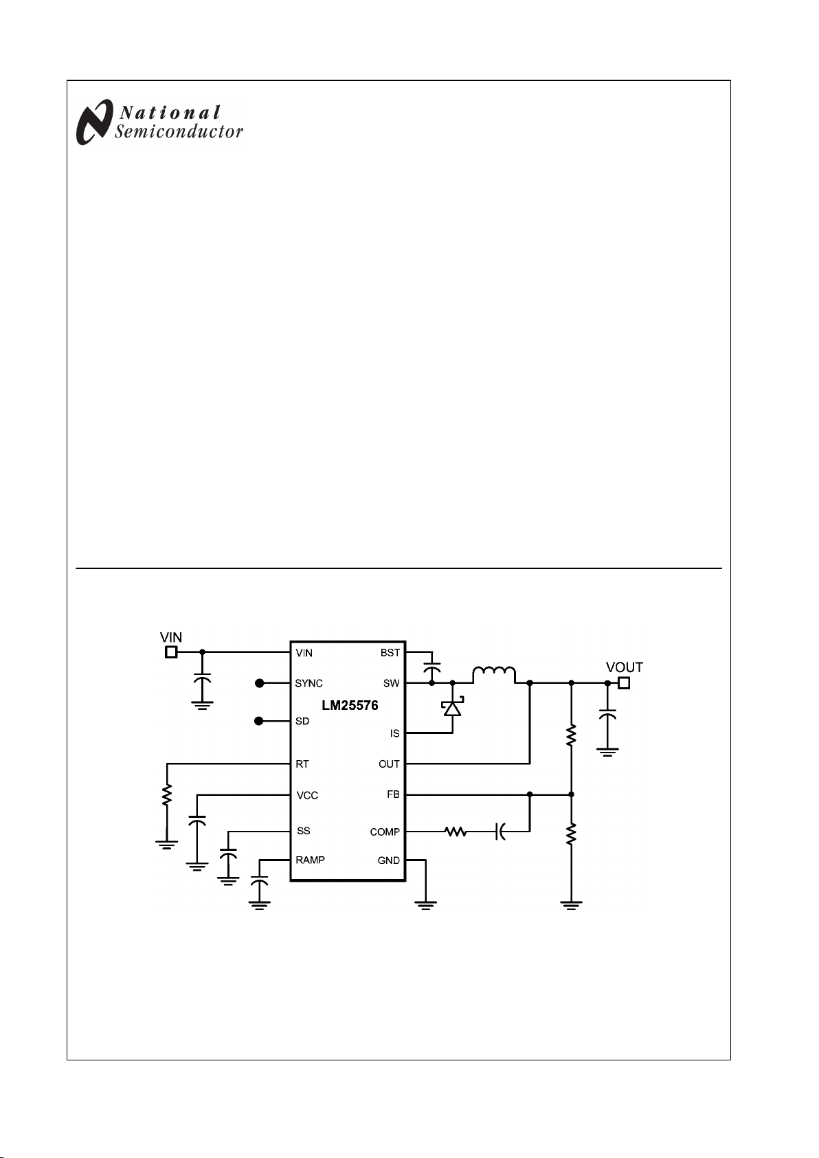
Simplified Application Schematic
20208701
WEBENCH® is a registered trademark of National Semiconductor Corporation.
© 2007 National Semiconductor Corporation 202087 www.national.com
LM25576 SIMPLE SWITCHER® 42V, 3A Step-Down Switching Regulator
Page 2

Connection Diagram
20208702
Top View
20-Lead TSSOP
Ordering Information
Order Number Package Type NSC Package Drawing Supplied As
LM25576MH Exposed Pad TSSOP-20 MXA20A 73 Units in Rail
LM25576MHX Exposed Pad TSSOP-20 MXA20A 2500 Units on Tape and Reel
www.national.com 2
LM25576
Page 3

Pin Descriptions
Pin(s) Name Description Application Information
1 VCC Output of the bias regulator Vcc tracks Vin up to 9V. Beyond 9V, Vcc is regulated to 7
Volts. A 0.1uF to 1uF ceramic decoupling capacitor is
required. An external voltage (7.5V – 14V) can be applied
to this pin to reduce internal power dissipation.
2 SD Shutdown or UVLO input If the SD pin voltage is below 0.7V the regulator will be in a
low power state. If the SD pin voltage is between 0.7V and
1.225V the regulator will be in standby mode. If the SD pin
voltage is above 1.225V the regulator will be operational. An
external voltage divider can be used to set a line
undervoltage shutdown threshold. If the SD pin is left open
circuit, a 5µA pull-up current source configures the regulator
fully operational.
3, 4 Vin Input supply voltage Nominal operating range: 6V to 42V
5 SYNC Oscillator synchronization input or output The internal oscillator can be synchronized to an external
clock with an external pull-down device. Multiple LM25576
devices can be synchronized together by connection of their
SYNC pins.
6 COMP Output of the internal error amplifier The loop compensation network should be connected
between this pin and the FB pin.
7 FB Feedback signal from the regulated
output
This pin is connected to the inverting input of the internal
error amplifier. The regulation threshold is 1.225V.
8 RT Internal oscillator frequency set input The internal oscillator is set with a single resistor, connected
between this pin and the AGND pin.
9 RAMP Ramp control signal An external capacitor connected between this pin and the
AGND pin sets the ramp slope used for current mode
control. Recommended capacitor range 50pF to 2000pF.
10 AGND Analog ground Internal reference for the regulator control functions
11 SS Soft-start An external capacitor and an internal 10µA current source
set the time constant for the rise of the error amp reference.
The SS pin is held low during standby, Vcc UVLO and
thermal shutdown.
12 OUT Output voltage connection Connect directly to the regulated output voltage.
13, 14 PGND Power ground Low side reference for the PRE switch and the IS sense
resistor.
15, 16 IS Current sense Current measurement connection for the re-circulating
diode. An internal sense resistor and a sample/hold circuit
sense the diode current near the conclusion of the off-time.
This current measurement provides the DC level of the
emulated current ramp.
17, 18 SW Switching node The source terminal of the internal buck switch. The SW pin
should be connected to the external Schottky diode and to
the buck inductor.
19 PRE Pre-charge assist for the bootstrap
capacitor
This open drain output can be connected to SW pin to aid
charging the bootstrap capacitor during very light load
conditions or in applications where the output may be precharged before the LM25576 is enabled. An internal precharge MOSFET is turned on for 265ns each cycle just prior
to the on-time interval of the buck switch.
3 www.national.com
LM25576
Page 4

Pin(s) Name Description Application Information
20 BST Boost input for bootstrap capacitor An external capacitor is required between the BST and the
SW pins. A 0.022µF ceramic capacitor is recommended.
The capacitor is charged from Vcc via an internal diode
during the off-time of the buck switch.
NA EP Exposed Pad Exposed metal pad on the underside of the device. It is
recommended to connect this pad to the PWB ground plane,
in order to aid in heat dissipation.
www.national.com 4
LM25576
Page 5

Absolute Maximum Ratings (Note 1)
If Military/Aerospace specified devices are required,
please contact the National Semiconductor Sales Office/
Distributors for availability and specifications.
VIN to GND 45V
BST to GND 60V
PRE to GND 45V
SW to GND (Steady State) -1.5V
BST to V
CC
45V
SD, VCC to GND 14V
BST to SW 14V
OUT to GND Limited to Vin
SYNC, SS, FB, RAMP to GND 7V
ESD Rating (Note 2)
Human Body Model 2kV
Storage Temperature Range -65°C to +150°C
Operating Ratings (Note 1)
V
IN
6V to 42V
Operation Junction Temperature −40°C to + 125°C
Electrical Characteristics Specifications with standard typeface are for T
J
= 25°C, and those with boldface type
apply over full Operating Junction Temperature range. VIN = 24V, RT = 32.4kΩ unless otherwise stated. (Note 3)
Symbol Parameter Conditions Min Typ Max Units
STARTUP REGULATOR
VccReg Vcc Regulator Output 6.85 7.15 7.45 V
Vcc LDO Mode turn-off 9 V
Vcc Current Limit Vcc = 0V 25 mA
VCC SUPPLY
Vcc UVLO Threshold (Vcc increasing) 5.03 5.35 5.67 V
Vcc Undervoltage Hysteresis 0.25 V
Bias Current (Iin) FB = 1.3V 3.4 4.5 mA
Shutdown Current (Iin) SD = 0V 48 70 µA
SHUTDOWN THRESHOLDS
Shutdown Threshold (SD Increasing) 0.47 0.7 0.9 V
Shutdown Hysteresis 0.1 V
Standby Threshold (Standby Increasing) 1.17 1.225 1.28 V
Standby Hysteresis 0.1 V
SD Pull-up Current Source 5 µA
SWITCH CHARACTERSICS
Buck Switch Rds(on) 170 340
mΩ
BOOST UVLO 3.8 V
BOOST UVLO Hysteresis 0.56 V
Pre-charge Switch Rds(on) 70
Ω
Pre-charge Switch on-time 265 ns
CURRENT LIMIT
Cycle by Cycle Current Limit RAMP = 0V 3.6 4.2 5.1 A
Cycle by Cycle Current Limit Delay RAMP = 2.5V 100 ns
SOFT-START
SS Current Source 7 10 14 µA
OSCILLATOR
Frequency1 180 200 220 kHz
Frequency2
RT = 11kΩ
425 485 545 kHz
SYNC Source Impedance 11
kΩ
SYNC Sink Impedance 110
Ω
SYNC Threshold (falling) 1.3 V
SYNC Frequency
RT = 11kΩ
550 kHz
SYNC Pulse Width Minimum 15 ns
5 www.national.com
LM25576
Page 6

Symbol Parameter Conditions Min Typ Max Units
RAMP GENERATOR
Ramp Current 1 Vin = 36V, Vout=10V 136 160 184 µA
Ramp Current 2 Vin = 10V, Vout=10V 18 25 32 µA
PWM COMPARATOR
Forced Off-time 416 500 575 ns
Min On-time 80 ns
COMP to PWM Comparator Offset 0.7 V
ERROR AMPLIFIER
Feedback Voltage Vfb = COMP 1.207 1.225 1.243 V
FB Bias Current 17 nA
DC Gain 70 dB
COMP Sink / Source Current 3 mA
Unity Gain Bandwidth 3 MHz
DIODE SENSE RESISTANCE
D
SENSE
42
mΩ
THERMAL SHUTDOWN
Tsd Thermal Shutdown Threshold 165 °C
Thermal Shutdown Hysteresis 25 °C
THERMAL RESISTANCE
θ
JC
Junction to Case 6 °C/W
θ
JA
Junction to Ambient 40 °C/W
Note 1: Absolute Maximum Ratings are limits beyond which damage to the device may occur. Operating Ratings are conditions under which operation of the
device is intended to be functional. For guaranteed specifications and test conditions, see the Electrical Characteristics.
Note 2: The human body model is a 100pF capacitor discharged through a 1.5kΩ resistor into each pin.
Note 3: Min and Max limits are 100% production tested at 25°C. Limits over the operating temperature range are guaranteed through correlation using Statistical
Quality Control (SQC) methods. Limits are used to calculate National’s Average Outgoing Quality Level (AOQL).
Typical Performance Characteristics
Oscillator Frequency vs R
T
20208720
Oscillator Frequency vs Temperature
F
OSC
= 200kHz
20208721
www.national.com 6
LM25576
Page 7

Soft Start Current vs Temperature
20208722
VCC vs I
CC
VIN = 12V
20208723
VCC vs V
IN
RL = 7kΩ
20208724
Error Amplifier Gain/Phase
A
VCL
= 101
20208725
Demoboard Efficiency vs I
OUT
and V
IN
20208726
7 www.national.com
LM25576
Page 8

Typical Application Circuit and Block Diagram
20208703
FIGURE 1.
www.national.com 8
LM25576
Page 9

Detailed Operating Description
The LM25576 switching regulator features all of the functions
necessary to implement an efficient high voltage buck regulator using a minimum of external components. This easy to
use regulator integrates a 42V N-Channel buck switch with
an output current capability of 3 Amps. The regulator control
method is based on current mode control utilizing an emulated current ramp. Peak current mode control provides inherent
line voltage feed-forward, cycle-by-cycle current limiting, and
ease of loop compensation. The use of an emulated control
ramp reduces noise sensitivity of the pulse-width modulation
circuit, allowing reliable processing of very small duty cycles
necessary in high input voltage applications. The operating
frequency is user programmable from 50kHz to 1MHz. An
oscillator synchronization pin allows multiple LM25576 regulators to self synchronize or be synchronized to an external
clock. The output voltage can be set as low as 1.225V. Fault
protection features include, current limiting, thermal shutdown
and remote shutdown capability. The device is available in the
TSSOP-20 package featuring an exposed pad to aid thermal
dissipation.
The functional block diagram and typical application of the
LM25576 are shown in Figure 1. The LM25576 can be applied
in numerous applications to efficiently step-down a high, unregulated input voltage. The device is well suited for telecom,
industrial and automotive power bus voltage ranges.
High Voltage Start-Up Regulator
The LM25576 contains a dual-mode internal high voltage
startup regulator that provides the Vcc bias supply for the
PWM controller and boot-strap MOSFET gate driver. The input pin (VIN) can be connected directly to the input voltage,
as high as 42 Volts. For input voltages below 9V, a low
dropout switch connects Vcc directly to Vin. In this supply
range, Vcc is approximately equal to Vin. For Vin voltage
greater than 9V, the low dropout switch is disabled and the
Vcc regulator is enabled to maintain Vcc at approximately 7V.
The wide operating range of 6V to 42V is achieved through
the use of this dual mode regulator.
The output of the Vcc regulator is current limited to 25mA.
Upon power up, the regulator sources current into the capacitor connected to the VCC pin. When the voltage at the VCC
pin exceeds the Vcc UVLO threshold of 5.35V and the SD pin
is greater than 1.225V, the output switch is enabled and a softstart sequence begins. The output switch remains enabled
until Vcc falls below 5.0V or the SD pin falls below 1.125V.
An auxiliary supply voltage can be applied to the VCC pin to
reduce the IC power dissipation. If the auxiliary voltage is
greater than 7.3V, the internal regulator will essentially
shut off, reducing the IC power dissipation. The Vcc regulator
series pass transistor includes a diode between Vcc and Vin
that should not be forward biased in normal operation. Therefore the auxiliary Vcc voltage should never exceed the Vin
voltage.
In high voltage applications extra care should be taken to ensure the VIN pin does not exceed the absolute maximum
voltage rating of 45V. During line or load transients, voltage
ringing on the Vin line that exceeds the Absolute Maximum
Ratings can damage the IC. Both careful PC board layout and
the use of quality bypass capacitors located close to the VIN
and GND pins are essential.
20208704
FIGURE 2. Vin and Vcc Sequencing
9 www.national.com
LM25576
Page 10
Shutdown / Standby
The LM25576 contains a dual level Shutdown (SD) circuit.
When the SD pin voltage is below 0.7V, the regulator is in a
low current shutdown mode. When the SD pin voltage is
greater than 0.7V but less than 1.225V, the regulator is in
standby mode. In standby mode the Vcc regulator is active
but the output switch is disabled. When the SD pin voltage
exceeds 1.225V, the output switch is enabled and normal operation begins. An internal 5µA pull-up current source configures the regulator to be fully operational if the SD pin is left
open.
An external set-point voltage divider from VIN to GND can be
used to set the operational input range of the regulator. The
divider must be designed such that the voltage at the SD pin
will be greater than 1.225V when Vin is in the desired operating range. The internal 5µA pull-up current source must be
included in calculations of the external set-point divider. Hysteresis of 0.1V is included for both the shutdown and standby
thresholds. The SD pin is internally clamped with a 1kΩ resistor and an 8V zener clamp. The voltage at the SD pin
should never exceed 14V. If the voltage at the SD pin exceeds
8V, the bias current will increase at a rate of 1 mA/V.
The SD pin can also be used to implement various remote
enable / disable functions. Pulling the SD pin below the 0.7V
threshold totally disables the controller. If the SD pin voltage
is above 1.225V the regulator will be operational.
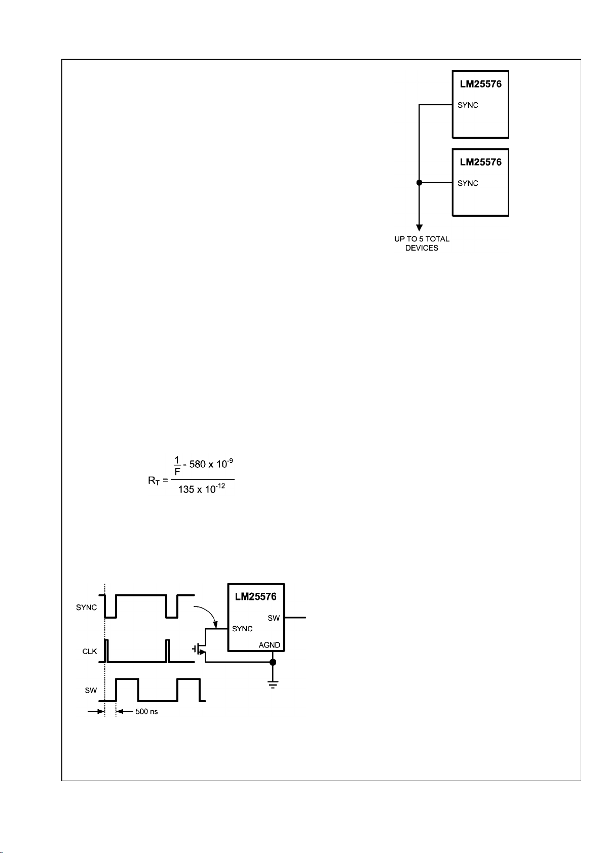
Oscillator and Sync Capability
The LM25576 oscillator frequency is set by a single external
resistor connected between the RT pin and the AGND pin.
The RT resistor should be located very close to the device and
connected directly to the pins of the IC (RT and AGND).To
set a desired oscillator frequency (F), the necessary value for
the RT resistor can be calculated from the following equation:
The SYNC pin can be used to synchronize the internal oscillator to an external clock. The external clock must be of
higher frequency than the free-running frequency set by the
RT resistor. A clock circuit with an open drain output is the
recommended interface from the external clock to the SYNC
pin. The clock pulse duration should be greater than 15ns.
20208705
FIGURE 3. Sync from External Clock
20208706
FIGURE 4. Sync from Multiple Devices
Multiple LM25576 devices can be synchronized together simply by connecting the SYNC pins together. In this configuration all of the devices will be synchronized to the highest
frequency device. The diagram in Figure 5 illustrates the
SYNC input/output features of the LM25576. The internal oscillator circuit drives the SYNC pin with a strong pull-down /
weak pull-up inverter. When the SYNC pin is pulled low either
by the internal oscillator or an external clock, the ramp cycle
of the oscillator is terminated and a new oscillator cycle begins. Thus, if the SYNC pins of several LM25576 IC’s are
connected together, the IC with the highest internal clock frequency will pull the connected SYNC pins low first and terminate the oscillator ramp cycles of the other IC’s. The LM25576
with the highest programmed clock frequency will serve as
the master and control the switching frequency of the all the
devices with lower oscillator frequency.
www.national.com 10
LM25576
Page 11

20208707
FIGURE 5. Simplified Oscillator Block Diagram and SYNC I/O Circuit
Error Amplifier and PWM
Comparator
The internal high gain error amplifier generates an error signal
proportional to the difference between the regulated output
voltage and an internal precision reference (1.225V). The
output of the error amplifier is connected to the COMP pin
allowing the user to provide loop compensation components,
generally a type II network, as illustrated in Figure 1. This
network creates a pole at DC, a zero and a noise reducing
high frequency pole. The PWM comparator compares the
emulated current sense signal from the RAMP generator to
the error amplifier output voltage at the COMP pin.
RAMP Generator
The ramp signal used in the pulse width modulator for current
mode control is typically derived directly from the buck switch
current. This switch current corresponds to the positive slope
portion of the output inductor current. Using this signal for the
PWM ramp simplifies the control loop transfer function to a
single pole response and provides inherent input voltage
feed-forward compensation. The disadvantage of using the
buck switch current signal for PWM control is the large leading
edge spike due to circuit parasitics that must be filtered or
blanked. Also, the current measurement may introduce significant propagation delays. The filtering, blanking time and
propagation delay limit the minimum achievable pulsewidth.
In applications where the input voltage may be relatively large
in comparison to the output voltage, controlling small
pulsewidths and duty cycles is necessary for regulation. The
LM25576 utilizes a unique ramp generator, which does not
actually measure the buck switch current but rather reconstructs the signal. Reconstructing or emulating the inductor
current provides a ramp signal to the PWM comparator that
is free of leading edge spikes and measurement or filtering
delays. The current reconstruction is comprised of two elements; a sample & hold DC level and an emulated current
ramp.
11 www.national.com
LM25576
Page 12

20208708
FIGURE 6. Composition of Current Sense Signal
The sample & hold DC level illustrated in Figure 6 is derived
from a measurement of the re-circulating Schottky diode anode current. The re-circulating diode anode should be connected to the IS pin. The diode current flows through an
internal current sense resistor between the IS and PGND
pins. The voltage level across the sense resistor is sampled
and held just prior to the onset of the next conduction interval
of the buck switch. The diode current sensing and sample &
hold provide the DC level of the reconstructed current signal.
The positive slope inductor current ramp is emulated by an
external capacitor connected from the RAMP pin to AGND
and an internal voltage controlled current source. The ramp
current source that emulates the inductor current is a function
of the Vin and Vout voltages per the following equation:
I
RAMP
= (5µ x (Vin – Vout)) + 25µA
Proper selection of the RAMP capacitor depends upon the
selected value of the output inductor. The value of C
RAMP
can
be selected from: C
RAMP
= L x 10-5, where L is the value of
the output inductor in Henrys. With this value, the scale factor
of the emulated current ramp will be approximately equal to
the scale factor of the DC level sample and hold ( 0.5 V / A).
The C
RAMP
capacitor should be located very close to the device and connected directly to the pins of the IC (RAMP and
AGND).
For duty cycles greater than 50%, peak current mode control
circuits are subject to sub-harmonic oscillation. Sub-harmonic
oscillation is normally characterized by observing alternating
wide and narrow pulses at the switch node. Adding a fixed
slope voltage ramp (slope compensation) to the current sense
signal prevents this oscillation. The 25µA of offset current
provided from the emulated current source adds some fixed
slope to the ramp signal. In some high output voltage, high
duty cycle applications, additional slope may be required. In
these applications, a pull-up resistor may be added between
the VCC and RAMP pins to increase the ramp slope compensation.
For V
OUT
> 7.5V:
Calculate optimal slope current, IOS = V
OUT
x 5µA/V.
For example, at V
OUT
= 10V, IOS = 50µA.
Install a resistor from the RAMP pin to VCC:
R
RAMP
= VCC / (IOS - 25µA)
20208745
FIGURE 7. R
RAMP
to VCC for V
OUT
> 7.5V
www.national.com 12
LM25576
Page 13

Maximum Duty Cycle / Input Dropout Voltage
There is a forced off-time of 500ns implemented each cycle
to guarantee sufficient time for the diode current to be sampled. This forced off-time limits the maximum duty cycle of the
buck switch. The maximum duty cycle will vary with the operating frequency.
D
MAX
= 1 - Fs x 500ns
Where Fs is the oscillator frequency. Limiting the maximum
duty cycle will raise the input dropout voltage. The input
dropout voltage is the lowest input voltage required to maintain regulation of the output voltage. An approximation of the
input dropout voltage is:
Where VD is the voltage drop across the re-circulatory diode.
Operating at high switching frequency raises the minimum input voltage necessary to maintain regulation.
Current Limit
The LM25576 contains a unique current monitoring scheme
for control and over-current protection. When set correctly,
the emulated current sense signal provides a signal which is
proportional to the buck switch current with a scale factor of
0.5 V / A. The emulated ramp signal is applied to the current
limit comparator. If the emulated ramp signal exceeds 2.1V
(4.2A) the present current cycle is terminated (cycle-by-cycle
current limiting). In applications with small output inductance
and high input voltage the switch current may overshoot due
to the propagation delay of the current limit comparator. If an
overshoot should occur, the diode current sampling circuit will
detect the excess inductor current during the off-time of the
buck switch. If the sample & hold DC level exceeds the 2.1V
current limit threshold, the buck switch will be disabled and
skip pulses until the diode current sampling circuit detects the
inductor current has decayed below the current limit threshold. This approach prevents current runaway conditions due
to propagation delays or inductor saturation since the inductor
current is forced to decay following any current overshoot.
Soft-Start
The soft-start feature allows the regulator to gradually reach
the initial steady state operating point, thus reducing start-up
stresses and surges. The internal soft-start current source,
set to 10µA, gradually increases the voltage of an external
soft-start capacitor connected to the SS pin. The soft-start
capacitor voltage is connected to the reference input of the
error amplifier. Various sequencing and tracking schemes
can be implemented using external circuits that limit or clamp
the voltage level of the SS pin.
In the event a fault is detected (over-temperature, Vcc UVLO,
SD) the soft-start capacitor will be discharged. When the fault
condition is no longer present a new soft-start sequence will
commence.
Boost Pin
The LM25576 integrates an N-Channel buck switch and associated floating high voltage level shift / gate driver. This gate
driver circuit works in conjunction with an internal diode and
an external bootstrap capacitor. A 0.022µF ceramic capacitor,
connected with short traces between the BST pin and SW pin,
is recommended. During the off-time of the buck switch, the
SW pin voltage is approximately -0.5V and the bootstrap capacitor is charged from Vcc through the internal bootstrap
diode. When operating with a high PWM duty cycle, the buck
switch will be forced off each cycle for 500ns to ensure that
the bootstrap capacitor is recharged.
Under very light load conditions or when the output voltage is
pre-charged, the SW voltage will not remain low during the
off-time of the buck switch. If the inductor current falls to zero
and the SW pin rises, the bootstrap capacitor will not receive
sufficient voltage to operate the buck switch gate driver. For
these applications, the PRE pin can be connected to the SW
pin to pre-charge the bootstrap capacitor. The internal precharge MOSFET and diode connected between the PRE pin
and PGND turns on each cycle for 265ns just prior to the onset
of a new switching cycle. If the SW pin is at a normal negative
voltage level (continuous conduction mode), then no current
will flow through the pre-charge MOSFET/diode.
Thermal Protection
Internal Thermal Shutdown circuitry is provided to protect the
integrated circuit in the event the maximum junction temperature is exceeded. When activated, typically at 165°C, the
controller is forced into a low power reset state, disabling the
output driver and the bias regulator. This feature is provided
to prevent catastrophic failures from accidental device overheating.
13 www.national.com
LM25576
Page 14

Application Information
EXTERNAL COMPONENTS
The procedure for calculating the external components is illustrated with the following design example. The Bill of Materials for this design is listed in Table 1. The circuit shown in
Figure 1 is configured for the following specifications:
•
V
OUT
= 5V
•
VIN = 7V to 42V
•
Fs = 300kHz
•
Minimum load current (for CCM) = 250mA
•
Maximum load current = 3A
R3 (RT)
RT sets the oscillator switching frequency. Generally, higher
frequency applications are smaller but have higher losses.
Operation at 300kHz was selected for this example as a reasonable compromise for both small size and high efficiency.
The value of RT for 300kHz switching frequency can be calculated as follows:
The nearest standard value of 21kΩ was chosen for RT.
L1
The inductor value is determined based on the operating frequency, load current, ripple current, and the minimum and
maximum input voltage (V
IN(min)
, V
IN(max)
).
20208710
FIGURE 8. Inductor Current Waveform
To keep the circuit in continuous conduction mode (CCM), the
maximum ripple current I
RIPPLE
should be less than twice the
minimum load current, or 0.5Ap-p. Using this value of ripple
current, the value of inductor (L1) is calculated using the following:
This procedure provides a guide to select the value of L1. The
nearest standard value (33µH) will be used. L1 must be rated
for the peak current (I
PK+
) to prevent saturation. During normal
loading conditions, the peak current occurs at maximum load
current plus maximum ripple. During an overload condition
the peak current is limited to 4.2A nominal (5.1A maximum).
The selected inductor (see Table 1) has a conservative 6.2
Amp saturation current rating. For this manufacturer, the saturation rating is defined as the current necessary for the
inductance to reduce by 30%, at 20°C.
C3 (C
RAMP
)
With the inductor value selected, the value of C3 (C
RAMP
)
necessary for the emulation ramp circuit is:
C
RAMP
= L x 10
-5
Where L is in Henrys
With L1 selected for 33µH the recommended value for C3 is
330pF.
C9, C10
The output capacitors, C9 and C10, smooth the inductor ripple current and provide a source of charge for transient loading conditions. For this design a 22µF ceramic capacitor and
a 150µF SP organic capacitor were selected. The ceramic
capacitor provides ultra low ESR to reduce the output ripple
voltage and noise spikes, while the SP capacitor provides a
large bulk capacitance in a small volume for transient loading
conditions. An approximation for the output ripple voltage is:
D1
A Schottky type re-circulating diode is required for all
LM25576 applications. Ultra-fast diodes are not recommended and may result in damage to the IC due to reverse recovery
current transients. The near ideal reverse recovery characteristics and low forward voltage drop are particularly important diode characteristics for high input voltage and low output
voltage applications common to the LM25576. The reverse
recovery characteristic determines how long the current
surge lasts each cycle when the buck switch is turned on. The
reverse recovery characteristics of Schottky diodes minimize
the peak instantaneous power in the buck switch occurring
during turn-on each cycle. The resulting switching losses of
the buck switch are significantly reduced when using a Schottky diode. The reverse breakdown rating should be selected
for the maximum VIN, plus some safety margin.
The forward voltage drop has a significant impact on the conversion efficiency, especially for applications with a low output
voltage. “Rated” current for diodes vary widely from various
manufacturers. The worst case is to assume a short circuit
load condition. In this case the diode will carry the output current almost continuously. For the LM25576 this current can
be as high as 4.2A. Assuming a worst case 1V drop across
the diode, the maximum diode power dissipation can be as
high as 4.2W. For the reference design a 60V Schottky in a
DPAK package was selected.
C1, C2
The regulator supply voltage has a large source impedance
at the switching frequency. Good quality input capacitors are
necessary to limit the ripple voltage at the VIN pin while supplying most of the switch current during the on-time. When the
buck switch turns on, the current into the VIN pin steps to the
lower peak of the inductor current waveform, ramps up to the
peak value, then drops to zero at turn-off. The average current
into VIN during the on-time is the load current. The input ca-
www.national.com 14
LM25576
Page 15

pacitance should be selected for RMS current rating and
minimum ripple voltage. A good approximation for the required ripple current rating necessary is I
RMS
> I
OUT
/ 2.
Quality ceramic capacitors with a low ESR should be selected
for the input filter. To allow for capacitor tolerances and voltage effects, two 2.2µF, 100V ceramic capacitors will be used.
If step input voltage transients are expected near the maximum rating of the LM25576, a careful evaluation of ringing
and possible spikes at the device VIN pin should be completed. An additional damping network or input voltage clamp
may be required in these cases.
C8
The capacitor at the VCC pin provides noise filtering and stability for the VCC regulator. The recommended value of C8
should be no smaller than 0.1µF, and should be a good quality, low ESR, ceramic capacitor. A value of 0.47µF was selected for this design.
C7
The bootstrap capacitor between the BST and the SW pins
supplies the gate current to charge the buck switch gate at
turn-on. The recommended value of C7 is 0.022µF, and
should be a good quality, low ESR, ceramic capacitor.
C4
The capacitor at the SS pin determines the soft-start time, i.e.
the time for the reference voltage and the output voltage, to
reach the final regulated value. The time is determined from:
For this application, a C4 value of 0.01µF was chosen which
corresponds to a soft-start time of 1ms.
R5, R6
R5 and R6 set the output voltage level, the ratio of these resistors is calculated from:
R5/R6 = (V
OUT
/ 1.225V) - 1
For a 5V output, the R5/R6 ratio calculates to 3.082. The resistors should be chosen from standard value resistors, a
good starting point is selection in the range of 1.0kΩ - 10kΩ.
Values of 5.11kΩ for R5, and 1.65kΩ for R6 were selected.
R1, R2, C12
A voltage divider can be connected to the SD pin to set a
minimum operating voltage Vin
(min)
for the regulator. If this
feature is required, the easiest approach to select the divider
resistor values is to select a value for R1 (between 10kΩ and
100kΩ recommended) then calculate R2 from:
Capacitor C12 provides filtering for the divider. The voltage at
the SD pin should never exceed 8V, when using an external
set-point divider it may be necessary to clamp the SD pin at
high input voltage conditions. The reference design utilizes
the full range of the LM25576 (6V to 42V); therefore these
components can be omitted. With the SD pin open circuit the
LM25576 responds once the Vcc UVLO threshold is satisfied.
R7, C11
A snubber network across the power diode reduces ringing
and spikes at the switching node. Excessive ringing and
spikes can cause erratic operation and couple spikes and
noise to the output. Voltage spikes beyond the rating of the
LM25576 or the re-circulating diode can damage these devices. Selecting the values for the snubber is best accomplished through empirical methods. First, make sure the lead
lengths for the snubber connections are very short. For the
current levels typical for the LM25576 a resistor value between 5 and 20 Ohms is adequate. Increasing the value of
the snubber capacitor results in more damping but higher
losses. Select a minimum value of C11 that provides adequate damping of the SW pin waveform at high load.
R4, C5, C6
These components configure the error amplifier gain characteristics to accomplish a stable overall loop gain. One advantage of current mode control is the ability to close the loop with
only two feedback components, R4 and C5. The overall loop
gain is the product of the modulator gain and the error amplifier gain. The DC modulator gain of the LM25576 is as follows:
DC Gain
(MOD)
= G
m(MOD)
x R
LOAD
= 2 x R
LOAD
The dominant low frequency pole of the modulator is determined by the load resistance (R
LOAD
,) and output capacitance
(C
OUT
). The corner frequency of this pole is:
f
p(MOD)
= 1 / (2π R
LOAD COUT
)
For R
LOAD
= 5Ω and C
OUT
= 177µF then f
p(MOD)
= 180Hz
DC Gain
(MOD)
= 2 x 5 = 10 = 20dB
For the design example of Figure 1 the following modulator
gain vs. frequency characteristic was measured as shown in
Figure 9.
20208715
FIGURE 9. Gain and Phase of Modulator
R
LOAD
= 5 Ohms and C
OUT
= 177µF
Components R4 and C5 configure the error amplifier as a type
II configuration which has a pole at DC and a zero at fZ = 1 /
15 www.national.com
LM25576
Page 16

(2πR4C5). The error amplifier zero cancels the modulator
pole leaving a single pole response at the crossover frequency of the loop gain. A single pole response at the crossover
frequency yields a very stable loop with 90 degrees of phase
margin.
For the design example, a target loop bandwidth (crossover
frequency) of 20kHz was selected. The compensation network zero (fZ) should be selected at least an order of magnitude less than the target crossover frequency. This constrains
the product of R4 and C5 for a desired compensation network
zero 1 / (2π R4 C5) to be less than 2kHz. Increasing R4, while
proportionally decreasing C5, increases the error amp gain.
Conversely, decreasing R4 while proportionally increasing
C5, decreases the error amp gain. For the design example
C5 was selected for 0.01µF and R4 was selected for
49.9kΩ. These values configure the compensation network
zero at 320Hz. The error amp gain at frequencies greater than
fZ is: R4 / R5, which is approximately 10 (20dB).
20208716
FIGURE 10. Error Amplifier Gain and Phase
The overall loop can be predicted as the sum (in dB) of the
modulator gain and the error amp gain.
20208717
FIGURE 11. Overall Loop Gain and Phase
If a network analyzer is available, the modulator gain can be
measured and the error amplifier gain can be configured for
the desired loop transfer function. If a network analyzer is not
available, the error amplifier compensation components can
be designed with the guidelines given. Step load transient
tests can be performed to verify acceptable performance. The
step load goal is minimum overshoot with a damped response. C6 can be added to the compensation network to
decrease noise susceptibility of the error amplifier. The value
of C6 must be sufficiently small since the addition of this capacitor adds a pole in the error amplifier transfer function. This
pole must be well beyond the loop crossover frequency. A
good approximation of the location of the pole added by C6
is: fp2 = fz x C5 / C6.
BIAS POWER DISSIPATION REDUCTION
Buck regulators operating with high input voltage can dissipate an appreciable amount of power for the bias of the IC.
The VCC regulator must step-down the input voltage VIN to a
nominal VCC level of 7V. The large voltage drop across the
VCC regulator translates into a large power dissipation within
the Vcc regulator. There are several techniques that can significantly reduce this bias regulator power dissipation. Figure
12 and Figure 13 depict two methods to bias the IC from the
output voltage. In each case the internal Vcc regulator is used
to initially bias the VCC pin. After the output voltage is established, the VCC pin potential is raised above the nominal 7V
regulation level, which effectively disables the internal V
CC
regulator. The voltage applied to the VCC pin should never
exceed 14V. The VCC voltage should never be larger than the
VIN voltage.
www.national.com 16
LM25576
Page 17

20208718
FIGURE 12. VCC Bias from VOUT for 8V < VOUT < 14V
20208719
FIGURE 13. VCC Bias with Additional Winding on the Output Inductor
17 www.national.com
LM25576
Page 18

PCB LAYOUT AND THERMAL CONSIDERATIONS
The circuit in Figure 13 serves as both a block diagram of the
LM25576 and a typical application board schematic for the
LM25576. In a buck regulator there are two loops where currents are switched very fast. The first loop starts from the input
capacitors, to the regulator VIN pin, to the regulator SW pin,
to the inductor then out to the load. The second loop starts
from the output capacitor ground, to the regulator PGND pins,
to the regulator IS pins, to the diode anode, to the inductor
and then out to the load. Minimizing the loop area of these
two loops reduces the stray inductance and minimizes noise
and possible erratic operation. A ground plane in the PC
board is recommended as a means to connect the input filter
capacitors to the output filter capacitors and the PGND pins
of the regulator. Connect all of the low power ground connections (CSS, RT, C
RAMP
) directly to the regulator AGND pin.
Connect the AGND and PGND pins together through the topside copper area covering the entire underside of the device.
Place several vias in this underside copper area to the ground
plane.
The two highest power dissipating components are the recirculating diode and the LM25576 regulator IC. The easiest
method to determine the power dissipated within the
LM25576 is to measure the total conversion losses (Pin –
Pout) then subtract the power losses in the Schottky diode,
output inductor and snubber resistor. An approximation for
the Schottky diode loss is P = (1-D) x Iout x Vfwd. An approximation for the output inductor power is P = I
OUT
2
x R x 1.1,
where R is the DC resistance of the inductor and the 1.1 factor
is an approximation for the AC losses. If a snubber is used,
an approximation for the damping resistor power dissipation
is P = Vin2 x Fsw x Csnub, where Fsw is the switching frequency and Csnub is the snubber capacitor. The regulator
has an exposed thermal pad to aid power dissipation. Adding
several vias under the device to the ground plane will greatly
reduce the regulator junction temperature. Selecting a diode
with an exposed pad will aid the power dissipation of the
diode.
The most significant variables that affect the power dissipated
by the LM25576 are the output current, input voltage and operating frequency. The power dissipated while operating near
the maximum output current and maximum input volatge can
be appreciable. The operating frequency of the LM25576
evaluation board has been designed for 300kHz. When operating at 3A output current with a 42V input the power
dissipation of the LM25576 regulator is approximately 1.9W.
The junction-to-ambient thermal resistance of the LM25576
will vary with the application. The most significant variables
are the area of copper in the PC board, the number of vias
under the IC exposed pad and the amount of forced air cooling
provided. Referring to the evaluation board artwork, the area
under the LM25576 (component side) is covered with copper
and there are 5 connection vias to the solder side ground
plane. Additional vias under the IC will have diminishing value
as more vias are added. The integrity of the solder connection
from the IC exposed pad to the PC board is critical. Excessive
voids will greatly diminish the thermal dissipation capacity.
The junction-to-ambient thermal resistance of the LM25576
mounted in the evaluation board varies from 45°C/W with no
airflow to 25°C/W with 900 LFM (Linear Feet per Minute). With
a 25°C ambient temperature and no airflow, the predicted
junction temperature for the LM25576 will be 25 + (45 x 1.9)
= 110°C. If the evaluation board is operated at 3A output current and 42V input voltage for a prolonged period of time the
thermal shutdown protection within the IC may activate. The
IC will turn off allowing the junction to cool, followed by restart
with the soft-start capacitor reset to zero.
www.national.com 18
LM25576
Page 19

TABLE 1. 5V, 3A Demo Board Bill of Materials
ITEM PART NUMBER DESCRIPTION VALUE
C 1 C4532X7R2A225M CAPACITOR, CER, TDK 2.2µ, 100V
C 2 C4532X7R2A225M CAPACITOR, CER, TDK 2.2µ, 100V
C 3 C0805C331G1GAC CAPACITOR, CER, KEMET 330p, 100V
C 4 C2012X7R2A103K CAPACITOR, CER, TDK 0.01µ, 100V
C 5 C2012X7R2A103K CAPACITOR, CER, TDK 0.01µ, 100V
C 6 OPEN NOT USED
C 7 C2012X7R2A223K CAPACITOR, CER, TDK 0.022µ, 100V
C 8 C2012X7R1C474M CAPACITOR, CER, TDK 0.47µ, 16V
C 9 C3225X7R1C226M CAPACITOR, CER, TDK 22µ, 16V
C 10 EEFHE0J151R CAPACITOR, SP, PANASONIC 150µ, 6.3V
C 11 C0805C331G1GAC CAPACITOR, CER, KEMET 330p, 100V
C 12 OPEN NOT USED
D 1 CSHD6-60C DIODE, 60V, CENTRAL
6CWQ10FN DIODE, 100V, IR (D1-ALT)
L 1 DR127-330 INDUCTOR, COOPER 33µH
R 1 OPEN NOT USED
R 2 OPEN NOT USED
R 3 CRCW08052102F RESISTOR
21kΩ
R 4 CRCW08054992F RESISTOR
49.9kΩ
R 5 CRCW08055111F RESISTOR
5.11kΩ
R 6 CRCW08051651F RESISTOR
1.65kΩ
R 7 CRCW2512100J RESISTOR 10, 1W
U 1 LM25576 REGULATOR, NATIONAL SEMICONDUCTOR
19 www.national.com
LM25576
Page 20

PCB Layout
20208729
Component Side
20208730
Solder Side
20208731
Silkscreen
www.national.com 20
LM25576
Page 21

Typical Schematic for High Frequency (1MHz) Application
20208740
Schematic 3.3V, 3A, 1MHz
Typical Schematic for Buck/Boost (Inverting) Application
20208742
21 www.national.com
LM25576
Page 22
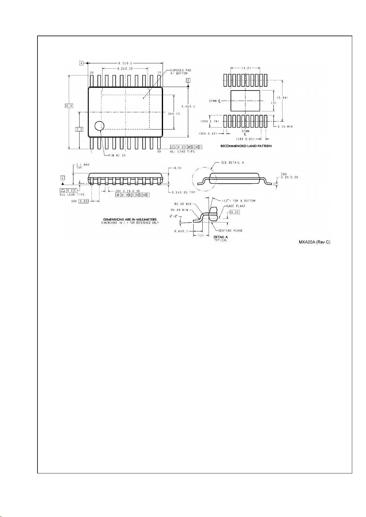
Physical Dimensions inches (millimeters) unless otherwise noted
20-Lead TSSOP Package
NS Package Number MXA20A
www.national.com 22
LM25576
Page 23

Notes
23 www.national.com
LM25576
Page 24
Notes
LM25576 SIMPLE SWITCHER® 42V, 3A Step-Down Switching Regulator
THE CONTENTS OF THIS DOCUMENT ARE PROVIDED IN CONNECTION WITH NATIONAL SEMICONDUCTOR CORPORATION
(“NATIONAL”) PRODUCTS. NATIONAL MAKES NO REPRESENTATIONS OR WARRANTIES WITH RESPECT TO THE ACCURACY
OR COMPLETENESS OF THE CONTENTS OF THIS PUBLICATION AND RESERVES THE RIGHT TO MAKE CHANGES TO
SPECIFICATIONS AND PRODUCT DESCRIPTIONS AT ANY TIME WITHOUT NOTICE. NO LICENSE, WHETHER EXPRESS,
IMPLIED, ARISING BY ESTOPPEL OR OTHERWISE, TO ANY INTELLECTUAL PROPERTY RIGHTS IS GRANTED BY THIS
DOCUMENT.
TESTING AND OTHER QUALITY CONTROLS ARE USED TO THE EXTENT NATIONAL DEEMS NECESSARY TO SUPPORT
NATIONAL’S PRODUCT WARRANTY. EXCEPT WHERE MANDATED BY GOVERNMENT REQUIREMENTS, TESTING OF ALL
PARAMETERS OF EACH PRODUCT IS NOT NECESSARILY PERFORMED. NATIONAL ASSUMES NO LIABILITY FOR
APPLICATIONS ASSISTANCE OR BUYER PRODUCT DESIGN. BUYERS ARE RESPONSIBLE FOR THEIR PRODUCTS AND
APPLICATIONS USING NATIONAL COMPONENTS. PRIOR TO USING OR DISTRIBUTING ANY PRODUCTS THAT INCLUDE
NATIONAL COMPONENTS, BUYERS SHOULD PROVIDE ADEQUATE DESIGN, TESTING AND OPERATING SAFEGUARDS.
EXCEPT AS PROVIDED IN NATIONAL’S TERMS AND CONDITIONS OF SALE FOR SUCH PRODUCTS, NATIONAL ASSUMES NO
LIABILITY WHATSOEVER, AND NATIONAL DISCLAIMS ANY EXPRESS OR IMPLIED WARRANTY RELATING TO THE SALE
AND/OR USE OF NATIONAL PRODUCTS INCLUDING LIABILITY OR WARRANTIES RELATING TO FITNESS FOR A PARTICULAR
PURPOSE, MERCHANTABILITY, OR INFRINGEMENT OF ANY PATENT, COPYRIGHT OR OTHER INTELLECTUAL PROPERTY
RIGHT.
LIFE SUPPORT POLICY
NATIONAL’S PRODUCTS ARE NOT AUTHORIZED FOR USE AS CRITICAL COMPONENTS IN LIFE SUPPORT DEVICES OR
SYSTEMS WITHOUT THE EXPRESS PRIOR WRITTEN APPROVAL OF THE CHIEF EXECUTIVE OFFICER AND GENERAL
COUNSEL OF NATIONAL SEMICONDUCTOR CORPORATION. As used herein:
Life support devices or systems are devices which (a) are intended for surgical implant into the body, or (b) support or sustain life and
whose failure to perform when properly used in accordance with instructions for use provided in the labeling can be reasonably expected
to result in a significant injury to the user. A critical component is any component in a life support device or system whose failure to perform
can be reasonably expected to cause the failure of the life support device or system or to affect its safety or effectiveness.
National Semiconductor and the National Semiconductor logo are registered trademarks of National Semiconductor Corporation. All other
brand or product names may be trademarks or registered trademarks of their respective holders.
Copyright© 2007 National Semiconductor Corporation
For the most current product information visit us at www.national.com
National Semiconductor
Americas Customer
Support Center
Email:
new.feedback@nsc.com
Tel: 1-800-272-9959
National Semiconductor Europe
Customer Support Center
Fax: +49 (0) 180-530-85-86
Email: europe.support@nsc.com
Deutsch Tel: +49 (0) 69 9508 6208
English Tel: +49 (0) 870 24 0 2171
Français Tel: +33 (0) 1 41 91 8790
National Semiconductor Asia
Pacific Customer Support Center
Email: ap.support@nsc.com
National Semiconductor Japan
Customer Support Center
Fax: 81-3-5639-7507
Email: jpn.feedback@nsc.com
Tel: 81-3-5639-7560
www.national.com
 Loading...