

Page 1
LM2524D/LM3524D
Regulating Pulse Width Modulator
General Description
The LM3524D family is an improved version of the industry
standard LM3524. It has improved specifications and additional featuresyet is pin for pin compatible with existing 3524
families. New features reduce the need for additional external circuitry often required in the original version.
The LM3524D has a
rent carrying capability of the output drive transistors has
been raised to 200 mAwhile reducing V
V
breakdown to 60V. The common mode voltage range of
CE
the error-amp has been raised to 5.5V to eliminate the need
for a resistive divider from the 5V reference.
In the LM3524D the circuit bias line has been isolated from
the shut-down pin. This prevents the oscillator pulse amplitude andfrequency from beingdisturbed by shut-down.Also
at high frequencies (
put has been improved to 44%compared to 35%max. duty
cycle in other 3524s.
In addition, the LM3524D can now be synchronized externally, through pin 3. Also a latch has been added to insure
±
1%precision 5V reference. The cur-
and increasing
CEsat
≅
300 kHz) the max. duty cycle per out-
one pulse per period even in noisy environments. The
LM3524D includes double pulse suppression logic that insures when a shut-down condition is removed the state of
the T-flip-flop will change only after the first clock pulse has
arrived. This feature prevents the same output from being
pulsed twice in a row, thus reducing the possibility of core
saturation in push-pull designs.
Features
n Fully interchangeable with standard LM3524 family
±
n
1%precision 5V reference with thermal shut-down
n Output current to 200 mA DC
n 60V output capability
n Wide common mode input range for error-amp
n One pulse per period (noise suppression)
n Improved max. duty cycle at high frequencies
n Double pulse suppression
n Synchronize through pin 3
LM2524D/LM3524D Regulating Pulse Width Modulator
June 1999
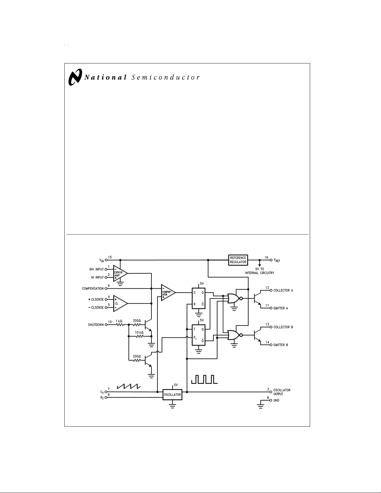
Block Diagram
DS008650-1
© 1999 National Semiconductor Corporation DS008650 www.national.com
Page 2
Absolute Maximum Ratings (Note 5)
If Military/Aerospace specified devices are required,
please contact the National Semiconductor Sales Office/
Distributors for availability and specifications.
Supply Voltage 40V
Collector Supply Voltage
(LM2524D) 55V
(LM3524D) 40V
Output Current DC (each) 200 mA
Internal Power Dissipation 1W
Operating Junction Temperature
Range (Note 2)
LM2524D −40˚C to +125˚C
LM3524D 0˚C to +125˚C
Maximum Junction Temperature 150˚
Storage Temperature Range −65˚C to +150˚C
Lead Temperature (Soldering 4 sec.)
M, N Pkg. 260˚C
Oscillator Charging Current (Pin 7) 5 mA
Electrical Characteristics
(Note 1)
Symbol Parameter Conditions Tested Design Tested Design Units
REFERENCE SECTION
V
V
V
REF
RLine
RLoad
Output Voltage 5 4.85 4.80 5 4.75 V
=
Line Regulation V
Load Regulation I
8V to 40V 10 15 30 10 25 50 mV
IN
=
0mAto20mA 10 15 25 10 25 50 mV
L
Ripple Rejection f=120 Hz 66 66 dB
LM2524D LM3524D
Typ Limit Limit Typ Limit Limit
(Note 3) (Note 4) (Note 3) (Note 4)
5.15 5.20 5.25 V
Min
Max
Max
Max
I
OS
Short Circuit V
Current 50 50
N
O
Output Noise 10 Hz ≤ f ≤ 10 kHz 40 100 40 100 µV
Long Term T
Stability
OSCILLATOR SECTION
f
f
OSC
OSC
Max. Freq. R
Initial R
Accuracy (Note 7) 20 20
∆f
OSC
∆f
OSC
Freq. Change V
with V
IN
Freq. Change T
with Temp. at 20 kHz R
V
OSC
Output Amplitude R
(Pin 3) (Note 8)
t
PW
Output Pulse R
Width (Pin 3)
Sawtooth Peak R
Voltage
Sawtooth Valley R
Voltage
ERROR-AMP SECTION
V
IO
Input Offset V
Voltage
I
IB
Input Bias V
=
0 25 25 mA Min
REF
180 200 mA Max
=
125˚C 20 20 mV/kHr
A
=
=
1k, C
T
0.001 µF 550 500 350 kHz
T
(Note 7)
=
T
=
5.6k, C
0.01 µF 17.5 17.5 kHz
T
22.5 22.5 kHz
=
R
T
=
2.7k, C
0.01 µF 34 30 kHz
T
(Note 7) 38 38
42 46 kHz
=
8 to 40V 0.5 1 0.5 1.0
IN
=
−55˚C to +125˚C
A
C
T
T
T
T
T
CM
CM
=
5.6k, 5 5
T
=
0.01 µF
=
=
=
=
=
5.6k, C
0.01 µF 3 2.4 3 2.4 V
T
=
5.6k, C
0.01 µF 0.5 1.5 0.5 1.5 µs
T
=
5.6k, C
0.01 µF 3.4 3.6 3.8 3.8 V
T
=
5.6k, C
0.01 µF 1.1 0.8 0.6 0.6 V
T
=
2.5V 2 8 10 210 mV
=
2.5V 1 8 10 110 µA
rms Max
Max
Max
%
Max
%
Min
Max
Max
Min
Max
Max
Min
Min
Min
www.national.com 2
Page 3
Electrical Characteristics (Continued)
(Note 1)
Symbol Parameter Conditions Tested Design Tested Design Units
ERROR-AMP SECTION
Current
I
IO
Input Offset V
=
2.5V 0.5 1.0 1 0.5 1 µA
CM
Current
I
COSI
Compensation V
IN(I)−VIN(NI)
=
150 mV 65 65 µA
Current (Sink) 95 95
I
COSO
Compensation V
IN(NI)−VIN(I)
=
150 mV −125 −125 µA
Current (Source) −95 −95
=
=
A
VOL
Open Loop Gain R
∞
,V
L
2.5 V 80 74 60 80 70 60 dB
CM
VCMR Common Mode 1.5 1.4 1.5 V
Input Voltage Range 5.5 5.4 5.5 V
CMRR Common Mode 90 80 90 80 dB
Rejection Ratio
G
BW
Unity Gain A
VOL
=
0 dB, V
=
2.5V 3 2 MHz
CM
Bandwidth
=
V
O
Output Voltage R
∞
L
Swing 5.5 5.5 V
PSRR Power Supply V
=
8 to 40V 80 70 80 65 db
IN
Rejection Ratio
COMPARATOR SECTION
Minimum Duty Pin 9=0.8V,
Cycle [R
=
T
5.6k, C
T
=
0.01 µF]
Maximum Duty Pin 9=3.9V,
Cycle [R
=
T
5.6k, C
T
=
0.01 µF]
Maximum Duty Pin 9=3.9V,
=
1k, C
=
T
0.001 µF]
V
COMPZ
Cycle [R
T
Input Threshold Zero Duty Cycle 1 1 V
(Pin 9)
V
COMPM
Input Threshold Maximum Duty Cycle 3.5 3.5 V
(Pin 9)
I
IB
Input Bias −1 −1 µA
Current
CURRENT LIMIT SECTION
V
SEN
Sense Voltage V
(Pin 2)−V(Pin 1)
≥ 180 180 mV
150 mV 200 200
TC-V
Sense Voltage T.C. 0.2 0.2 mV/˚C
sense
Common Mode −0.7 −0.7 V
Voltage Range V5−V
=
300 mV 1 1 V
4
SHUT DOWN SECTION
V
SD
High Input V
(Pin 2)−V(Pin 1)
≥ 1 0.5 1 0.5 V
Voltage 150 mV 1.5 1.5 V
I
SD
High Input I
(pin 10)
Current
OUTPUT SECTION (EACH OUTPUT)
V
CES
Collector Emitter IC≤ 100 µA 55 40 V
Voltage Breakdown
LM2524D LM3524D
Typ Limit Limit Typ Limit Limit
(Note 3) (Note 4) (Note 3) (Note 4)
125 125 µA
−65 −65 µA
0.5 0.5 V
00 0 0
49 45 49 45
44 35 44 35
220 220 mV
11 mA
Max
Min
Max
Min
Max
Min
Min
Max
Min
Min
Max
Min
%
Max
%
Min
%
Min
Min
Max
Min
Max
Min
Max
Min
www.national.com3
Page 4
Electrical Characteristics (Continued)
(Note 1)
Symbol Parameter Conditions Tested Design Tested Design Units
OUTPUT SECTION (EACH OUTPUT)
I
CES
V
V
CESAT
EO
Collector Leakage V
Current V
Saturation I
Voltage I
Emitter Output I
=
60V
CE
=
55V 0.1 50 µA
CE
=
V
40V 0.1 50
CE
=
20 mA 0.2 0.5 0.2 0.7 V
E
=
200 mA 1.5 2.2 1.5 2.5
E
=
50 mA 18 17 18 17 V
E
Voltage
t
R
t
F
Rise Time V
Fall Time R
=
20V,
IN
=
−250 µA 200 200 ns
I
E
=
2k
R
C
=
2k 100 100 ns
C
SUPPLY CHARACTERISTICS SECTION
V
IN
Input Voltage After Turn-on 8 8 V
Range 40 40 V
T Thermal Shutdown (Note 2) 160 160 ˚C
Temp.
=
20V and f
=
40V (Note 6) 5 10 5 10 mA
IN
=
20 kHz.
OSC
=
=
T
25˚C. Boldface numbers applyover the rated temperaturerange: LM2524D is −40˚to85˚C
A
J
I
IN
Note 1: Unless otherwise stated, thesespecificationsapply for T
and LM3524D is 0˚C to 70˚C. V
Note 2: For operation at elevated temperatures,devices in the N package must be derated based on a thermal resistance of 86˚C/W, junction to ambient. Devices
in the M package must be derated at 125˚C/W, junction to ambient.
Note 3: Tested limits are guaranteed and 100%tested in production.
Note 4: Design limits are guaranteed (but not 100%production tested) over the indicated temperature and supply voltage range. These limits are not used to cal-
culate outgoing quality level.
Note 5: Absolute maximum ratings indicate limitsbeyond which damage to the device mayoccur. DC andAC electrical specifications do notapply when operating
the device beyond its rated operating conditions.
Note 6: Pins 1, 4, 7, 8, 11, and 14 are grounded; Pin 2=2V.All other inputs and outputs open.
Note 7: The value of a C
in this test. NPO ceramic or polypropylene can also be used.
Note 8: OSC amplitude is measured open circuit. Available current is limited to 1 mAso care must be exercised to limit capacitive loading of fast pulses.
Stand By Current V
IN
capacitor can vary with frequency. Careful selection of this capacitor must be made for high frequency operation. Polystyrene was used
t
LM2524D LM3524D
Typ Limit Limit Typ Limit Limit
(Note 3) (Note 4) (Note 3) (Note 4)
Max
Max
Min
Min
Max
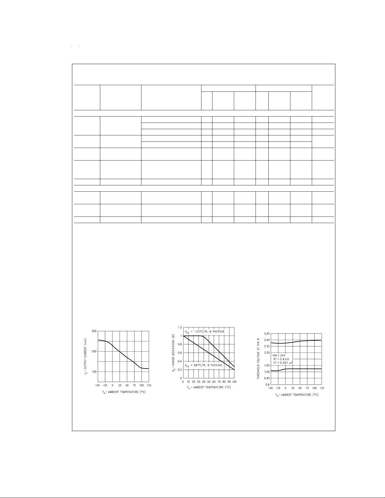
Typical Performance Characteristics
Switching Transistor
Peak Output Current
vs Temperature
DS008650-28
www.national.com 4
Maximum Average Power
Dissipation (N, M Packages)
Maximum & Minimum
Duty Cycle Threshold
Voltage
DS008650-29
DS008650-30
Page 5
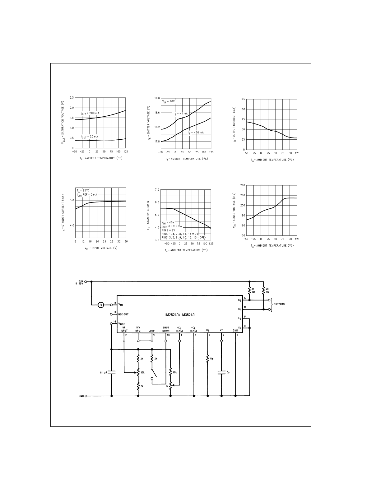
Typical Performance Characteristics (Continued)
Output Transistor
Saturation Voltage
Standby Current
vs Voltage
DS008650-31
DS008650-34
Output Transistor Emitter
Voltage
Standby Current
vs Temperature
DS008650-32
DS008650-35
Reference Transistor
Peak Output Current
DS008650-33
Current Limit Sense Voltage
DS008650-36
Test Circuit
DS008650-4
www.national.com5
Page 6
Functional Description
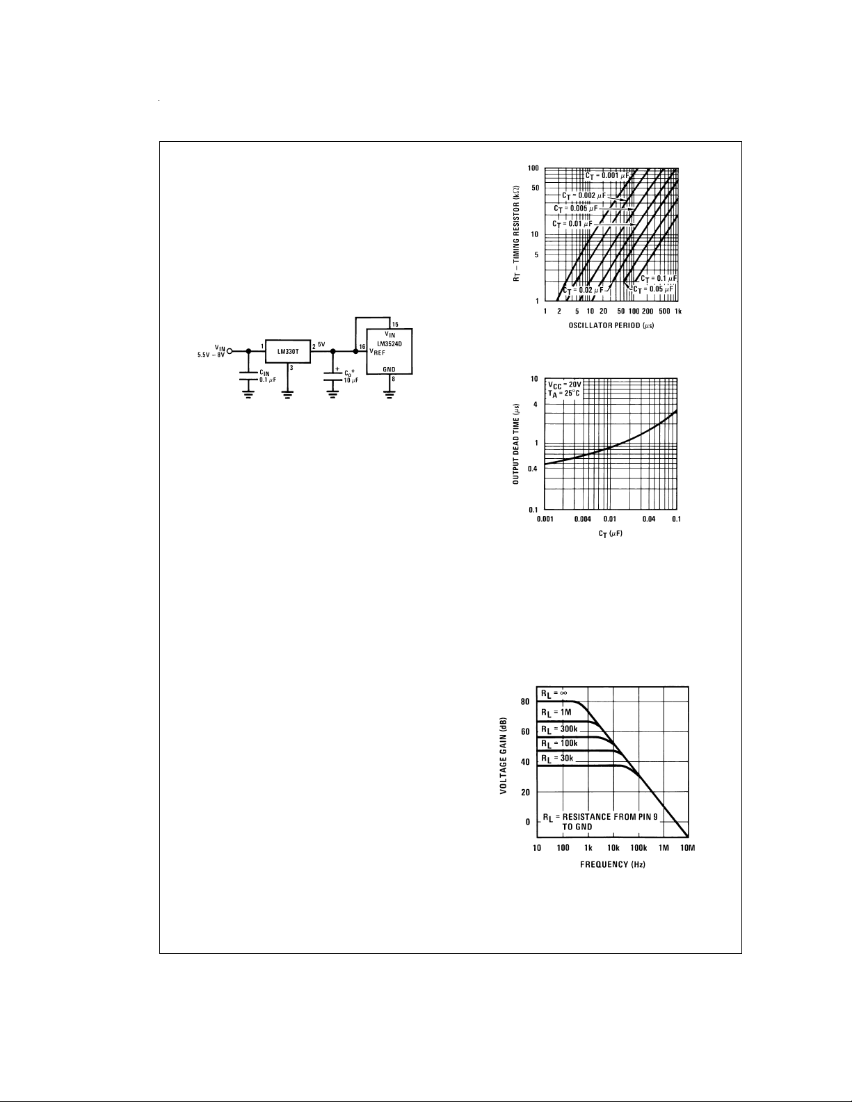
INTERNAL VOLTAGE REGULATOR
The LM3524D has an on-chip 5V, 50 mA, short circuit protected voltage regulator. This voltage regulator provides a
supply for all internal circuitry ofthe device and can be used
as an external reference.
For input voltages of less than 8V the 5V output should be
shorted to pin 15, V
these pins shorted the input voltage must be limited to a
maximum of6V. If input voltages of 6V–8V are to be used, a
pre-regulator, as shown in
, which disables the 5V regulator. With
IN
Figure 1
, must be added.
DS008650-5
FIGURE 2.
*Minimum COof 10 µF required for stability.
DS008650-10
FIGURE 1.
OSCILLATOR
The LM3524D provides a stable on-board oscillator. Its frequency isset by an external resistor, R
graph of R
The oscillator’s output provides the signals for triggering an
vs oscillator frequency is shown is
T,CT
and capacitor, CT.A
T
Figure 2
internal flip-flop, which directs the PWM information to the
outputs, and a blanking pulse to turn off both outputs during
transitions to ensure that cross conduction does not occur.
The width of the blanking pulse, or dead time, is controlled
by thevalue of C
values of R
0.1 µF.
, asshown in
T
are 1.8 kΩ to 100 kΩ, and for CT, 0.001 µF to
T
Figure 3
. The recommended
If two or more LM3524D’s must be synchronized together,
the easiest method is to interconnect all pin 3 terminals, tie
all pin 7’s (together)to asingle C
except one which is connected to a single R
works well unless the LM3524D’s are more than 6" apart.
, and leave allpin 6’sopen
T
. This method
T
A second synchronization method is appropriate for any circuit layout.One LM3524D,designated asmaster, must have
its R
LM3524D(s) should each have an R
period. All pin 3’s must then be interconnected to allow the
set for the correct period. The other slave
TCT
set for a 10%longer
TCT
master to properly reset the slave units.
The oscillator may be synchronized to an external clock
source by setting the internal free-running oscillator frequency 10%slower than the external clock and driving pin 3
with a pulse train (approx. 3V) from the clock. Pulse width
should be greater than 50 ns to insure full synchronization.
.
FIGURE 3.
ERROR AMPLIFIER
The error amplifier is a differential input, transconductance
amplifier. Its gain, nominally 86dB, is set by either feedback
or output loading. This output loading can be done with either purely resistive or a combination of resistive and reactive components. A graph of the amplifier’s gain vs output
load resistance is shown in
Figure 4
.
DS008650-6
www.national.com 6
DS008650-7
FIGURE 4.
The output of the amplifier, or input to the pulse width modulator, can be overridden easily as its output impedance is
very high (Z
≅
5MΩ). For this reason a DC voltage can be
O
Page 7

Functional Description (Continued)
applied to pin 9 which will override the error amplifier and
force a particular duty cycle to the outputs. An example of
this could be a non-regulating motor speed control where a
variable voltage was applied topin 9 tocontrol motor speed.
A graph of the output duty cycle vs the voltage on pin 9 is
shown in
Figure 5
.
The duty cycle is calculated as the percentage ratio of each
output’s ON-time tothe oscillator period. Paralleling the outputs doubles the observed duty cycle.
DS008650-8
FIGURE 5.
The amplifier’s inputs have a common-mode input range of
1.5V–5.5V. The on board regulator is useful for biasing the
inputs to within this range.
CURRENT LIMITING
The function of the current limit amplifier is to override the error amplifier’soutput andtake control of the pulsewidth. The
output duty cycle drops to about 25%when a current limit
sense voltage of 200 mV is applied between the +C
−C
sense terminals. Increasing the sense voltage approxi-
L
mately 5%results in a 0%output duty cycle. Care shouldbe
and
L
taken to ensure the −0.7V to +1.0V input common-mode
range is not exceeded.
In most applications, the current limit sense voltage is produced by a currentthrough asense resistor. The accuracy of
this measurement is limited bythe accuracy ofthe sense resistor, and by asmall offset current, typically 100µA, flowing
from +CL to −CL.
OUTPUT STAGES
The outputs of theLM3524D areNPN transistors,capable of
a maximum current of 200 mA. These transistors are driven
180˚ out of phase and have non-committed open collectors
and emitters as shown in
Figure 6
.
DS008650-9
FIGURE 6.
www.national.com7
Page 8

Typical Applications
DS008650-11
FIGURE 7. Positive Regulator, Step-Up Basic Configuration (I
FIGURE 8. Positive Regulator, Step-Up Boosted Current Configuration
www.national.com 8
IN(MAX)
=
80 mA)
DS008650-12
Page 9

Typical Applications (Continued)
DS008650-13
FIGURE 9. Positive Regulator, Step-Down Basic Configuration (I
IN(MAX)
FIGURE 10. Positive Regulator, Step-Down Boosted Current Configuration
=
80 mA)
DS008650-14
www.national.com9
Page 10

Typical Applications (Continued)
FIGURE 11. Boosted Current Polarity Inverter
BASIC SWITCHING REGULATOR THEORY
AND APPLICATIONS
The basic circuit of a step-down switching regulator circuit is
shown in
ing the LM3524D in
Figure 12
, along with a practical circuit design us-
Figure 15
.
DS008650-15
The circuit works as follows: Q1 is used as a switch, which
has ON and OFF times controlled by the pulse width modulator. When Q1 isON, power is drawn from V
to the load through L1; V
verse biased, and C
ductor L1 will force V
it, D1 will start conducting and the load current will flow
through D1and L1. The voltage atV
C
filter giving a clean DC output. The current flowing
o
through L1 is equal to the nominal DC load current plus
some ∆I
good rule of thumb is to set
which is due to the changing voltage across it.
L
is at approximately VIN,D1isre-
A
is charging. When Q1 turnsOFF thein-
o
negative to keep the current flowing in
A
is smoothedby the L1,
A
≅
∆
I
LP-P
IN
40%xIo.
and supplied
A
DS008650-16
FIGURE 12. Basic Step-Down Switching Regulator
www.national.com 10
Page 11

Typical Applications (Continued)
FIGURE 13. Relation of Switch Timing to Inductor Current in Step-Down Regulator
+
−
Neglecting V
SAT,VD
, and settling ∆I
where T=Total Period
The above shows the relation between V
cycle.
as Q1 only conducts during tON.
=
∆I
L
L
IN,Vo
;
and duty
DS008650-17
where: L1 is in Henrys
f is switching frequency in Hz
Also, see LM1578 data sheetfor graphicalmethods ofinductor selection.
CALCULATING OUTPUT FILTER CAPACITOR C
Figure 13
t
OFF
flow to the load and C
ence between I
From
C
a time, t
∆I
shows L1’s current with respect to Q1’s tONand
times (VAis at the collector of Q1). This curent must
’s current will then be the differ-
o.Co
, and Io.
L
Figure 13
for the second half of tONthrough the first half of t
o
/4. The resulting ∆Vcor ∆Vois described by:
L
it can be seen that current will be flowinginto
/2+t
ON
OFF
=
Ic
I
o
L−Io
/2. The current flowing for this time is
:
o
,or
OFF
The efficiency, η, of the circuit is:
ηMAX will be further decreased due to switching losses in
Q1. Forthis reason Q1 should beselected to have the maximum possible f
, which implies very fast rise and fall times.
T
CALCULATING INDUCTOR L1
−
Since ∆IL+=∆I
=
0.4I
L
o
Solving the above for L1
For best regulation, the inductor’s current cannot be allowed
to fall to zero. Some minimum load current I
ductor current, is required as shown below:
, and thus in-
o
www.national.com11
Page 12

Typical Applications (Continued)
range. Since each output transistor is on for half the period,
actually 45%, they have been paralleledto allow longerpossible duty cycle, up to 90%. This makes a lower possible input voltage. The output voltage is set by:
DS008650-19
FIGURE 14. Inductor Current Slope in Step-Down
Regulator
A complete step-down switching regulator schematic, using
Figure 15
the LM3524D, is illustrated in
. TransistorsQ1 and
Q2 havebeen addedto boostthe outputto 1A.The 5V regulator of the LM3524D has beendivided in half to bias the error amplifier’snon-inverting input to within itscommon-mode
where VNIis thevoltage at theerror amplifier’s non-inverting
input.
Resistor R3 sets the current limit to:
Figures 16, 17
gram for the 5V, 1A regulator of
performance is listed in
and show a PC board layout and stuffingdia-
Table 1
Figure 15
.
. The regulator’s
*Mounted to Staver Heatsink No. V5-1.
Q1=BD344
Q2=2N5023
=
>
40 turns No. 22 wire on Ferroxcube No. K300502 Torroid core.
L1
FIGURE 15. 5V, 1 Amp Step-Down Switching Regulator
www.national.com 12
DS008650-20
Page 13

Typical Applications (Continued)
Parameter Conditions Typical
Output Voltage V
Switching Frequency V
Short Circuit V
Current Limit
Load Regulation V
Line Regulation ∆V
Efficiency V
Output Ripple V
TABLE 1.
=
IN
=
IN
=
IN
=
IN
=
I
o
IN
=
I
o
=
IN
=
IN
=
10V, I
10V, I
1A 5V
o
=
1A 20 kHz
o
10V 1.3A
10V 3 mV
0.2−1A
=
10 − 20V, 6 mV
1A
=
10V, I
10V, I
1A 80
o
=
1A 10 mVp-p
o
Characteristics
%
FIGURE 16. 5V, 1 Amp Switching Regulator, Foil Side
FIGURE 17. Stuffing Diagram, Component Side
DS008650-21
DS008650-22
www.national.com13
Page 14

Typical Applications (Continued)
THE STEP-UP SWITCHING REGULATOR
Figure 18
regulator. In this circuit Q1 is used as a switch to alternately
apply V
and energy is drawnfrom V
biased and I
Q1 opens, t
where D1 turns ON. The output current is now supplied
through L1, D1 to the load and any charge lost from C
ing t
lator,the current through L1 has a DCcomponent plussome
∆I
ure 19
and OFF times.
shows the basic circuit for a step-up switching
across inductor L1. During the time, tON,Q1isON
IN
is supplied from thecharge storedin Co. When
o
, voltage V1 will rise positively to the point
OFF
is replenished. Here also, as in the step-down regu-
ON
. ∆ILis again selected to be approximately 40%of IL.
L
shows the inductor’s current in relation to Q1’s ON
and stored in L1;D1 isreverse
IN
FIGURE 19. Relation of Switch Timing to Inductor Current in Step-Up Regulator
dur-
o
Fig-
DS008650-23
FIGURE 18. Basic Step-Up Switching Regulator
DS008650-24
Since ∆IL+=∆IL−, VINt
and neglecting V
SAT
The above equationshows the relationship between VIN,V
and duty cycle.
In calculating input current I
tor’s DC current, assume first 100%efficiency:
for η=100%,P
OUT
ON
and V
=
P
=
V
otOFF−VINtOFF
D1
, which equals the induc-
IN(DC)
IN
,
o
This equation shows that the input, or inductor, current is
larger than the output current by the factor (1 + t
Since this factor is the same as the relation between V
V
IN,IIN(DC)
www.national.com 14
can also be expressed as:
ON/tOFF
o
).
and
So far it isassumed η=100%, where the actualefficiency or
η
will be somewhat less due to the saturation voltage of
MAX
Q1 and forward on voltage of D1. The internal power loss
due to these voltagesis theaverage I
through either V
loss becomes I
or VD1. For V
SAT
IN(DC)
(1V). η
MAX
This equation assumes only DC losses, howeverη
ther decreased because of the switching time of Q1 and D1.
current flowing, or IIN,
L
=
=
V
SAT
is then:
1V this power
D1
MAX
is fur-
Page 15

Typical Applications (Continued)
In calculating the output capacitor C
supplies Ioduring tON. The voltage change on Coduring this
time will be some ∆V
lator. Calculation of C
=
∆V
c
o
is:
o
where: Cois in farads, f is the switching frequency,
is the p-p output ripple
∆V
o
Calculation of inductor L1 is as follows:
VINis applied across L1
it can be seen that C
o
or the output ripple of the regu-
where: L1 is in henrys, f is the switching frequency in Hz
To apply the above theory, a complete step-up switching
o
regulator is shown in
to V
. Theinput voltage is divided by 2 to bias the error am-
IN
plifier’s inverting input. The output voltage is:
Figure 20
. Since VINis 5V, V
The network D1, C1 forms a slow start circuit.
This holds the output of the error amplifier initially low thus
reducing theduty-cycle to a minimum. Without the slow start
circuit the inductor may saturate at turn-on because it has to
supply high peak currents to charge the output capacitor
from 0V. It should also be noted that this circuit has no supply rejection. By adding a reference voltage at the
non-inverting input to the error amplifier, see
input voltage variations are rejected.
The LM3524D can also be used in inductorless switching
regulators.
nected to
Figure 22
Figure 20
shows a polarity inverter which if con-
provides a −15V unregulated output.
REF
Figure 21
is tied
, the
www.national.com15
Page 16

Typical Applications (Continued)
=
>
L1
25 turns No. 24 wire on Ferroxcube No. K300502 Toroid core.
FIGURE 20. 15V, 0.5A Step-Up Switching Regulator
DS008650-26
FIGURE 21. Replacing R3/R4 Divider in
Reference Circuit Improves Line Regulation
Figure 20
with
DS008650-25
DS008650-27
FIGURE 22. Polarity Inverter Provides Auxiliary −15V
Unregulated Output from Circuit of
Figure 20
www.national.com 16
Page 17

Connection Diagram
DS008650-2
Top View
Order Number LM2524DN or LM3524DN
See NS Package Number N16E
Order Number LM3524DM
See NS Package Number M16A
www.national.com17
Page 18

Physical Dimensions inches (millimeters) unless otherwise noted
Molded Surface-Mount Package (M)
Order Number LM3524DM
NS Package Number M16A
www.national.com 18
Page 19

Physical Dimensions inches (millimeters) unless otherwise noted (Continued)
Molded Dual-In-Line Package (N)
Order Number LM2524DN or LM3524DN
NS Package Number N16E
LM2524D/LM3524D Regulating Pulse Width Modulator
LIFE SUPPORT POLICY
NATIONAL’S PRODUCTS ARE NOT AUTHORIZED FOR USE AS CRITICAL COMPONENTS IN LIFE SUPPORT
DEVICES OR SYSTEMS WITHOUT THE EXPRESS WRITTEN APPROVAL OF THE PRESIDENT AND GENERAL
COUNSEL OF NATIONAL SEMICONDUCTOR CORPORATION. As used herein:
1. Life support devices or systems are devices or
systems which, (a) are intended for surgical implant
into the body, or (b) support or sustain life, and
whose failure to perform when properly used in
accordance with instructions for use provided in the
2. A critical component is any component of a life
support device or system whose failure to perform
can be reasonably expected to cause the failure of
the life support device or system, or to affect its
safety or effectiveness.
labeling, can be reasonably expected to result in a
significant injury to the user.
National Semiconductor
Corporation
Americas
Tel: 1-800-272-9959
Fax: 1-800-737-7018
Email: support@nsc.com
www.national.com
National does not assume any responsibility for use of any circuitry described, no circuit patent licenses are implied and National reserves the right at any time without notice to change said circuitry and specifications.
National Semiconductor
Europe
Fax: +49 (0) 1 80-530 85 86
Email: europe.support@nsc.com
Deutsch Tel: +49 (0) 1 80-530 85 85
English Tel: +49 (0) 1 80-532 78 32
Français Tel: +49 (0) 1 80-532 93 58
Italiano Tel: +49 (0) 1 80-534 16 80
National Semiconductor
Asia Pacific Customer
Response Group
Tel: 65-2544466
Fax: 65-2504466
Email: sea.support@nsc.com
National Semiconductor
Japan Ltd.
Tel: 81-3-5639-7560
Fax: 81-3-5639-7507
 Loading...