

Page 1
LM2480
80V Triple Bias Clamp
General Description
The LM2480 driver is an Integrated 80V triple bias clamp
circuit for DC recovery of each of the AC coupled outputs of
a CRT driver. It is well matched with the DAC outputs of the
LM126X family of pre-amplifiers. Each amplifier has its gain
internally set to -18. The IC is packaged in an industry
standard 8 lead molded DIP package.
Features
n Wide range integrated triple bias clamp
n High input impedance
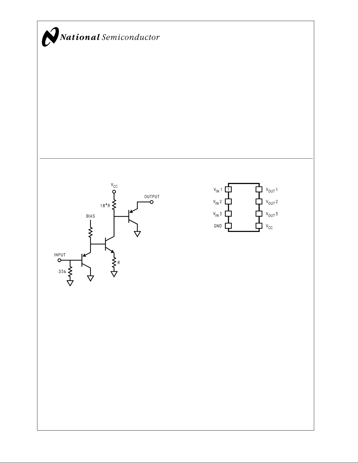
Block Diagrams Package Pinout
n Single supply operation
n Matched to the LM126X family of preamplifiers
Recommended Applications
n CRT monitors requiring DC restoration at the cathodes
LM2480 80V Triple Bias Clamp
October 2001
20008301
FIGURE 1. Simplified Schematic (One Channel)
20008302
FIGURE 2. LM2480 Package Pinout
Order Number LM2480NA
NS Package Number: N08E
© 2001 National Semiconductor Corporation DS200083 www.national.com
Page 2
Absolute Maximum Ratings (Note 1)
If Military/Aerospace specified devices are required,
LM2480
please contact the National Semiconductor Sales Office/
Distributors for availability and specifications.
Supply Voltage, V
Input Voltage, V
Storage Temperature Range, T
Lead Temperature (Soldering,
<
10sec.) 300˚C
CC
IN
STG
-65˚C to +150˚C
+90V
0V to 5V
Machine Model 200V
Human Body Model 2KV
Limits of Operating Ranges (Note 3)
V
CC
V
OUT
Ambient Temperature Range, T
A
ESD Tolerance
DC CLAMP ELECTRICAL CHARACTERISTICS TARGETS AND LIMIT
Unless otherwise noted: VCC= +80V, VIN= 2.25VDC,TA= 25˚C.
Symbol Spec Parameter Conditions Min Typ Max Units
I
CC
V
OUT
V
OUT-Range
V
OUTSAT
A
V
Supply Current All channels 2.1 3.5 mA
DC Output Voltage 42 46 50 V
Output Voltage Range VINRange = 1.0V - 4.0V 53 V
Max Saturation Limit VIN= 4.0V 16 V
DC Voltage Gain -16 -18 -20
LE Linearity Error See Note 1 5 %
R
IN
Note 1: Linearity Error is the variation in DC gain from VIN= 1.0V to VIN= 4.0V.
Note 2: Absolute Maximum Ratings indicate limits beyond which damage to the device may occur.
Note 3: Operating Ratingsindicateconditions for which the device is functional, but do not guarantee specific performance limits. For guaranteed specificationsand
the test conditions, see the Electrical Characteristics. The guaranteed specifications apply only for the test conditions listed. Some performance characteristics may
change when the device is not operated under the listed test conditions.
Note 4: All voltages are measured with respect to GND, unless otherwise specified.
Input Resistance 34K Ω
70V to 85V
10V to V
CC
0 to 70˚C
DC
DC
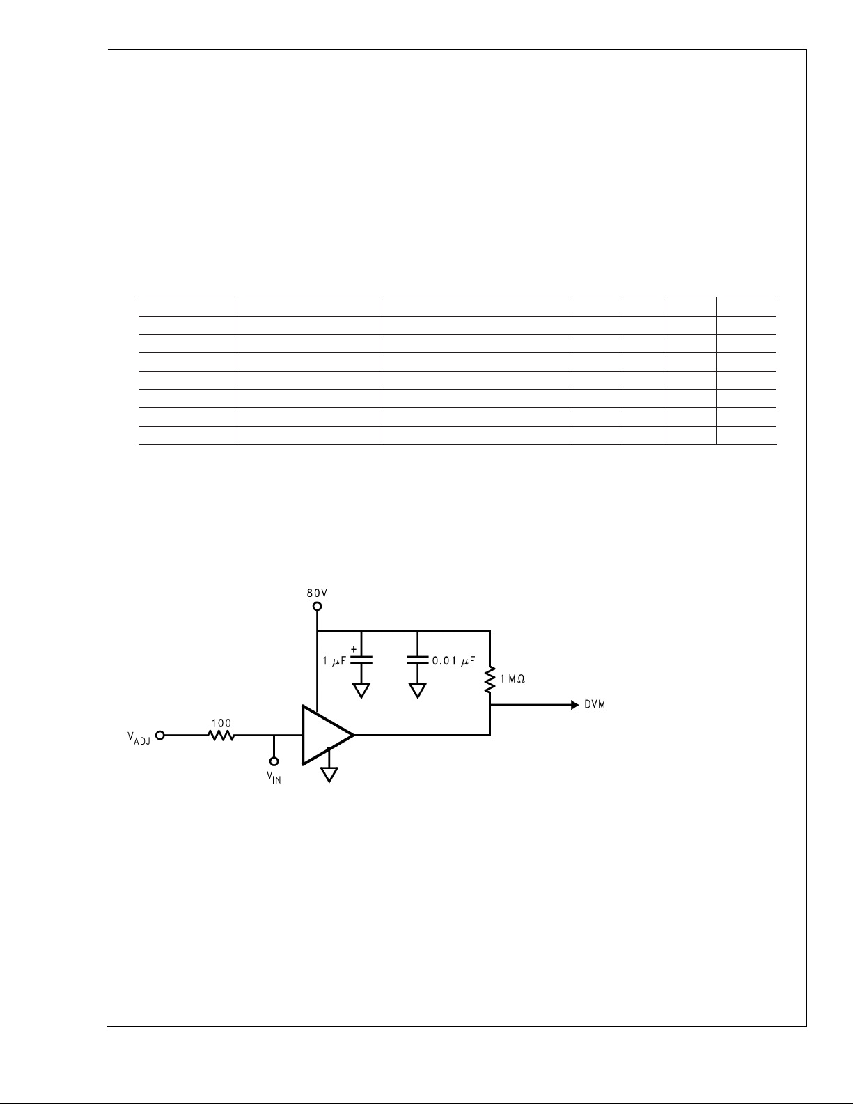
Test Circuit
Figure 3
measurements at the output.
shows the test circuit for evaluation of the LM2480 Clamp Amplifier. A high impedance VM (>100MΩ) is used for DC
20008303
FIGURE 3. Test Circuit (One Channel)
www.national.com 2
Page 3

Typical Performance Characteristics
(VCC= +80V), Test Circuit - Figure 3 unless otherwise specified.
20008304
the supply pin to ground. The electrolytic capacitor should
also be placed reasonably close to the LM2480’s supply and
ground pins.
Application Circuit
The application circuit shown in Figure 5 is designed to help
clamp the voltage at the output of the driver to the desired
level. Capacitor C
the clamp diode, D
stabilizes the entire node at the anode of
4
, by creating a low impedance at high
3
frequencies. Figure 5 also shows the standard application
circuit topology when used with an LM246X CRT driver. It
shows all the components necessary to optimize performance as well as to protect against damage from a CRT arc
event. No additional components are required to protect the
LM2480 from arc damage.
LM2480
FIGURE 4. V
out
vs V
in
THEORY OF OPERATION
The circuit diagram of the LM2480 is shown in Figure 1. The
DC clamp circuit amplifies the input signal by -18 and the
gain is set by the resistor ratio of 18R and R. The output
requires pull-up resistor to 80V. Figure 2 shows the test
circuit used for evaluation of the LM2480 Clamp Amplifier. A
high impedance voltmeter (
>
100MΩ) is used for DC measurements at the output. The DC transfer function is shown
in Figure 4.
APPLICATION HINTS
Power Supply Bypass
The LM2480 should have proper power supply bypassing for
optimum performance. A 0.1µF capacitor should be connected from the supply pin, V
supply and ground pins as is practical. Additionally, a 1.0µF
electrolycelectrolytictic capacitor should be connected from
, to ground, as close to the
cc
20008307
FIGURE 5. One Channel of the LM2480 and LM246X
Application Circuit
Demonstration Hardware
National Semiconductor has designed a demonstration
neckboard for the LM126X, LM246X, and the LM2480
chipset. To obtain demonstration boards contact the National
Semiconductor Sales Office in your region.
www.national.com3
Page 4

Physical Dimensions inches (millimeters)
unless otherwise noted
LM2480 80V Triple Bias Clamp
Molded Dual-In-Line Package (N)
NS Package Number N08E
Note: Information contained in this data sheet is preliminary and may be subject to change without notice.
LIFE SUPPORT POLICY
NATIONAL’S PRODUCTS ARE NOT AUTHORIZED FOR USE AS CRITICAL COMPONENTS IN LIFE SUPPORT
DEVICES OR SYSTEMS WITHOUT THE EXPRESS WRITTEN APPROVAL OF THE PRESIDENT AND GENERAL
COUNSEL OF NATIONAL SEMICONDUCTOR CORPORATION. As used herein:
1. Life support devices or systems are devices or
systems which, (a) are intended for surgical implant
into the body, or (b) support or sustain life, and
whose failure to perform when properly used in
accordance with instructions for use provided in the
2. A critical component is any component of a life
support device or system whose failure to perform
can be reasonably expected to cause the failure of
the life support device or system, or to affect its
safety or effectiveness.
labeling, can be reasonably expected to result in a
significant injury to the user.
National Semiconductor
Corporation
Americas
Email: support@nsc.com
www.national.com
National does not assume any responsibility for use of any circuitry described, no circuit patent licenses are implied and National reserves the right at any time without notice to change said circuitry and specifications.
National Semiconductor
Europe
Fax: +49 (0) 180-530 85 86
Email: europe.support@nsc.com
Deutsch Tel: +49 (0) 69 9508 6208
English Tel: +44 (0) 870 24 0 2171
Français Tel: +33 (0) 1 41 91 8790
National Semiconductor
Asia Pacific Customer
Response Group
Tel: 65-2544466
Fax: 65-2504466
Email: ap.support@nsc.com
National Semiconductor
Japan Ltd.
Tel: 81-3-5639-7560
Fax: 81-3-5639-7507
 Loading...