

Page 1
LM2426TE
Monolithic Triple Channel 30 MHz DTV Driver
LM2426TE Monolithic Triple Channel 30 MHz DTV Driver
May 2003
General Description
The LM2426TE is an integrated high voltage CRT driver
circuit designed for use in HDTV applications. The IC contains three high input impedance, wide band amplifiers
which directly drive the RGB cathodes of a CRT. Each
channel has its gain internally set to −53 and can drive CRT
capacitive loads as well as resistive loads present in other
applications, limited only by the package’s power dissipation.
The IC is packaged in an industry standard 11-lead TO-220
molded plastic power package designed specifically to meet
high voltage spacing requirements. See Thermal Considerations section.
Features
n 0V to 5V input range
n Greater than 130V
n Stable with 0– 20 pF capacitive loads and inductive
peaking networks
n Convenient TO-220 staggered thin lead package style
output swing capability
PP
Applications
n AC coupled HDTV applications using the 1080i and
720p formats as well as standard NTSC and PAL
formats.
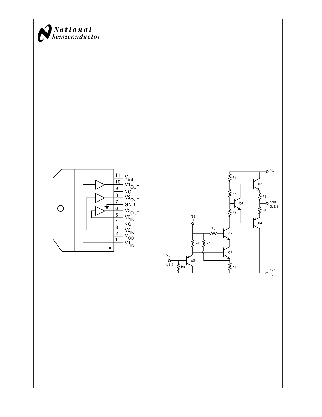
Connection Diagram Schematic Diagram
Note: Tab is at GND
Top View
Order Number LM2426TE
FIGURE 1. Simplified Connection and Pinout Diagram
© 2003 National Semiconductor Corporation DS200664 www.national.com
20066402
20066401
FIGURE 2. Simplified Schematic Diagram
(One Channel)
Page 2
Absolute Maximum Ratings (Notes 1,
3)
If Military/Aerospace specified devices are required,
LM2426TE
please contact the National Semiconductor Sales Office/
Distributors for availability and specifications.
Supply Voltage (V
Bias Voltage (V
Input Voltage (V
Storage Temperature Range (T
) +200V
CC
) +15V
BB
) -0.5V to VBB+0.5V
IN
) −65˚C to +150˚C
STG
Operating Ranges (Note 2)
V
CC
V
BB
V
IN
V
OUT
Case Temperature Refer to Figure 11
Do not operate the part without a heat sink.
+130V to +180V
+7V to +13V
+15V to +175V
Lead Temperature
(Soldering,
<
10 sec.) 300˚C
ESD Tolerance,
Human Body Model 2kV
Machine Model 200V
Junction Temperature 150˚C
θ
(typ) 2.9˚C/W
JC
Electrical Characteristics
(See Figure 3 for Test Circuit) Unless otherwise noted: VCC= +180V, VBB= +8V, CL= 8pF, TC= 50˚C. DC Tests: VIN=
. AC Tests: Output = 110VPP(55V - 165V) at 1MHz.
2.5V
DC
Symbol Parameter Conditions
I
CC
Supply Current All Three Channels, No Input Signal,
No Output Load
I
BB
V
OUT, 1
V
OUT, 2
A
V
∆A
V
Bias Current All Three Channels 15 22 mA
DC Output Voltage No AC Input Signal, VIN= 2.5V
DC Output Voltage No AC Input Signal, VIN= 1.2V
DC
DC
DC Voltage Gain No AC Input Signal -50 -53 -56
Gain Matching (Note 4), No AC Input Signal 1.0 dB
LE Linearity Error (Notes 4, 5), No AC Input Signal 8 %
t
R
t
F
Rise Time (Note 6), 10% to 90% 13 ns
Fall Time (Note 6), 90% to 10% 13 ns
OS Overshoot (Note 6) 7 %
Note 1: Absolute Maximum Ratings indicate limits beyond which damage to the device may occur.
Note 2: Operating ratings indicate conditions for which the device is functional, but do not guarantee specific performance limits. For guaranteed specifications and
test conditions, see the Electrical Characteristics. Datasheet min/max specification limits are guaranteed by design, test, or statistical analysis. The guaranteed
specifications apply only for the test conditions listed. Some performance characteristics may change when the device is not operated under the listed test
conditions.
Note 3: All voltages are measured with respect to GND, unless otherwise specified.
Note 4: Calculated value from Voltage Gain test on each channel.
Note 5: Linearity Error is the variation in DC gain from V
<
Note 6: Input from signal generator: t
r,tf
1 ns.
= 1.1V to VIN= 3.8V.
IN
LM2426TE
Min Typical Max
28 40 mA
93 98 103 V
160 165 170 V
+0V to +4V
Units
DC
DC
www.national.com 2
Page 3

AC Test Circuit
LM2426TE
Note: 8pF load includes parasitic capacitance.
FIGURE 3. Test Circuit (One Channel)
Figure 3 shows a typical test circuit for evaluation of the LM2426TE. This circuit is designed to allow testing of the LM2426TE in
a50Ω environment without the use of an expensive FET probe. The two 4990Ω resistors form a 400:1 divider with the 50Ω
resistor and the oscilloscope. A test point is included for easy use of an oscilloscope probe.The compensation capacitor is used
to compensate the network to achieve flat frequency response.
20066403
www.national.com3
Page 4
Typical Performance Characteristics (V
(55V − 165V), Test Circuit - Figure 3 unless otherwise specified)
LM2426TE
= +180VDC,VBB= +8VDC,CL= 8pF, V
CC
OUT
= 110V
PP
20066404
FIGURE 4. V
OUT
vs V
IN
20066406
FIGURE 5. LM2426TE Pulse Response
20066405
FIGURE 7. Speed vs Load Capacitance
20066408
FIGURE 8. Speed vs Offset
20066418
FIGURE 6. Bandwidth
www.national.com 4
20066409
FIGURE 9. Speed vs Case Temperature
Page 5

LM2426TE
Typical Performance Characteristics (V
= +180VDC,VBB= +8VDC,CL= 8pF, V
CC
(55V − 165V), Test Circuit - Figure 3 unless otherwise specified) (Continued)
FIGURE 10. Power Dissipation vs Frequency
20066407
OUT
= 110V
PP
20066416
FIGURE 11. Power Derating Curve
20066419
FIGURE 12. Cathode Pulse Response
www.national.com5
Page 6

Typical Performance Characteristics (V
= +180VDC,VBB= +8VDC,CL= 8pF, V
CC
(55V − 165V), Test Circuit - Figure 3 unless otherwise specified) (Continued)
OUT
= 110V
PP
LM2426TE
Note: Input from signal generator: tr,t
TABLE 1. Power Dissipation for Various Video Patterns
Power Dissipation (W)
Pattern Format
480i 480p 720p 1080i
Raster 2.4 2.4 2.4 2.4
Full White Field 6.1 6.1 6.0 6.5
White Box, 75% Screen Size 4.6 4.6 4.0 4.2
Gray Bars 4.8 4.8 4.7 5.0
Color Bars 75% Amplitude 3.9 4.0 4.0 4.1
Color Bars 100% Amplitude 4.3 4.3 4.3 4.5
SMPTE Color Bars 3.8 3.8 3.8 4.0
SMPTE 133 5.0 5.2 5.4 5.7
Cross Hatch 16x12 2.8 3.0 3.0 2.9
Resolution Chart 5.3 5.5 5.6 5.8
Multiburst 5.4 6.6 10.1 10.9
White Text on Black Background 5.2 7.1 11.1 12.3
Windows Pattern 4.0 4.5 6.4 6.6
Windows Pattern 4.7 5.2 6.7 7.0
Windows Pattern 6.0 6.7 8.6 9.4
Vertical Lines 5 On 5 Off 5.1 5.9 8.7 9.5
Vertical Lines 4 On 4 Off 5.3 6.3 9.8 10.8
Vertical Lines 3 On 3 Off 5.6 7.0 11.7 12.9
Vertical Lines 2 On 2 Off 6.3 8.5 14.4 16.2
Vertical Lines 1 On 1 Off 8.5 12.7 21.8 24.6
<
2 ns.
f
Theory of Operation
The LM2426TE is a high voltage monolithic three channel
CRT driver suitable for HDTV applications. The LM2426TE
operates with 180V and 8V power supplies. The part is
housed in the industry standard 11-lead TO-220 molded
plastic power package with thin leads for improved metal-tometal spacing.
The circuit diagram of the LM2426TE is shown in Figure 2.
The PNP emitter follower, Q5, provides input buffering. Q1
and Q2 form a fixed gain cascode amplifier with resistors R1
and R2 setting the gain at −53. Emitter followers Q3 and Q4
isolate the high output impedance of the cascode stage from
the capacitance of the CRT cathode which decreases the
sensitivity of the device to load capacitance. Q6 provides
biasing to the output emitter follower stage to reduce crossover distortion at low signal levels.
Figure 3 shows a typical test circuit for evaluation of the
LM2426TE. This circuit is designed to allow testing of the
LM2426TE in a 50Ω environment without the use of an
expensive FET probe. In this test circuit, the two 4.99kΩ
resistors form a 400:1 wideband, low capacitance probe
when connected to a 50Ω coaxial cable and a 50Ω load
(such as a 50Ω oscilloscope input). The input signal from the
generator is ac coupled to the base of Q5.
Application Hints
INTRODUCTION
National Semiconductor (NSC) is committed to provide application information that assists our customers in obtaining
the best performance possible from our products. The following information is provided in order to support this commitment. The reader should be aware that the optimization of
performance was done using a specific printed circuit board
designed at NSC. Variations in performance can be realized
due to physical changes in the printed circuit board and the
application. Therefore, the designer should know that component value changes may be required in order to optimize
performance in a given application. The values shown in this
document can be used as a starting point for evaluation
purposes. When working with high bandwidth circuits, good
layout practices are also critical to achieving maximum performance.
IMPORTANT INFORMATION
The LM2426TE performance is targeted for the HDTV market. The application circuits shown in this document to optimize performance and to protect against damage from CRT
arcover are designed specifically for the LM2426TE. If another member of the LM242X family is used, please refer to
its datasheet.
www.national.com 6
Page 7

Application Hints (Continued)
POWER SUPPLY BYPASS
Since the LM2426TE is a wide bandwidth amplifier, proper
power supply bypassing is critical for optimum performance.
Improper power supply bypassing can result in large overshoot, ringing or oscillation. 0.1µF capacitors should be connected from the supply pins, V
close to the LM2426TE as is practical.Additionally, a 22µF or
larger electrolytic capacitor should be connected from both
supply pins to ground reasonably close to the LM2426TE.
ARC PROTECTION
During normal CRT operation, internal arcing may occasionally occur. Spark gaps, in the range of 300V, connected from
the CRT cathodes to CRT ground will limit the maximum
voltage, but to a value that is much higher than allowable on
the LM2426TE. This fast, high voltage, high energy pulse
can damage the LM2426TE output stage. The application
circuit shown in Figure 13 is designed to help clamp the
voltage at the output of the LM2426TE to a safe level. The
clamp diodes, D1 and D2, should have a fast transient
response, high peak current rating, low series impedance
and low shunt capacitance. 1SS83 or equivalent diodes are
recommended. D1 and D2 should have short, low impedance connections to V
and ground respectively. The cath-
CC
ode of D1 should be located very close to a separately
decoupled bypass capacitor (C3 in Figure 13). The ground
connection of D2 and the decoupling capacitor should be
very close to the LM2426TE ground. This will significantly
reduce the high frequency voltage transients that the
LM2426TE would be subjected to during an arcover condition. Resistor R2 limits the arcover current that is seen by the
diodes while R1 limits the current into the LM2426TE as well
as the voltage stress at the outputs of the device. R2 should
1
⁄2W solid carbon type resistor. R1 can be a1⁄4W metal
be a
or carbon film type resistor. Having large value resistors for
R1 and R2 would be desirable, but this has the effect of
increasing rise and fall times. Inductor L1 is critical to reduce
the initial high frequency voltage levels that the LM2426TE
would be subjected to. The inductor will not only help protect
the device but it will also help minimize rise and fall times as
well as minimize EMI. For proper arc protection, it is important to not omit any of the arc protection components shown
in Figure 13.
and VBB, to ground, as
CC
EFFECT OF OFFSET
Figure 8 shows the variation in rise and fall times when the
output offset of the device is varied from 105 to 115V
DC
. The
rise time shows a variation of less than 7% relative to the
center data point (110V
). The fall time shows a variation of
DC
less than 2% relative to the center data point.
THERMAL CONSIDERATIONS
Figure 9 shows the performance of the LM2426TE in the test
circuit shown in Figure 3 as a function of case temperature.
The figure shows that the rise and fall times of the
LM2426TE increase by approximately 10% and 4%, respectively, as the case temperature increases from 50˚C to 90˚C.
This corresponds to a speed degradation of 2.5% and 1% for
every 10˚C rise in case temperature.
Figure 10 shows the power dissipation of the LM2426TE vs.
Frequency when all three channels of the device are driving
an 8pF load with a 110V
alternating one pixel on, one pixel
PP
off signal. The graph assumes a 72% active time (device
operating at the specified frequency) which is typical in a TV
application. The other 28% of the time the device is assumed
to be sitting at the black level (165V in this case). Table 1
also shows the typical power dissipation of the LM2426TE
for various video patterns in the 480i, 480p, 720p, and 1080i
video formats.
Figure 10, Figure 11, and Table 1 give the designer the
information needed to determine the heatsink requirement
for the LM2426TE. For example, if an HDTV application
uses the 720p format and "Vertical Lines 2 On 2 Off" is
assumed to be the worst-case pattern to be displayed, then
the power dissipated will be 14.4W (from Table 1). Figure 11
shows that the maximum allowed case temperature is 108˚C
when 14.4W is dissipated. If the maximum expected ambient
temperature is 70˚C, then a maximum heatsink thermal resistance can be calculated:
This example assumes a capacitive load of 8pF and no
resistive load. The designer should note that if the load
capacitance is increased the AC component of the total
power dissipation will also increase.
Note: An LM126X preamplifier, with rise and fall times of
about 2 ns, was used to drive the LM2426TE for these power
measurements. Using a preamplifier with rise and fall times
slower than the LM126X will cause the LM2426TE to dissipate less power than shown in Table 1.
LM2426TE
20066410
FIGURE 13. One Channel of the LM2426TE with the
Recommended Application Circuit
EFFECT OF LOAD CAPACITANCE
Figure 7 shows the effect of increased load capacitance on
the speed of the device. This demonstrates the importance
of knowing the load capacitance in the application.
OPTIMIZING TRANSIENT RESPONSE
In Figure 13, there are three components (R1, R2 and L1)
that can be adjusted to optimize the transient response of
the application circuit. Increasing the values of R1 and R2
will slow the circuit down while decreasing overshoot. Increasing the value of L1 will speed up the circuit as well as
increase overshoot. It is very important to use inductors with
very high self-resonant frequencies, preferably above 300
MHz. Ferrite core inductors from J.W. Miller Magnetics (part
#
78FR_ _k) were used for optimizing the performance of the
device in the NSC application board. The values shown in
Figure 14 and Figure 15 can be used as a good starting point
for the evaluation of the LM2426TE. Using a variable resistor
for R1 will simplify finding the value needed for optimum
performance in a given application. Once the optimum value
is determined, the variable resistor can be replaced with a
fixed value.
www.national.com7
Page 8

Application Hints (Continued)
Figure 12 shows the typical cathode pulse response with an
output swing of 110V
LM2426TE
PC BOARD LAYOUT CONSIDERATIONS
For optimum performance, an adequate ground plane, isolation between channels, good supply bypassing and minimizing unwanted feedback are necessary. Also, the length of
the signal traces from the preamplifier to the LM2426TE and
from the LM2426TE to the CRT cathode should be as short
as possible. The following references are recommended:
Ott, Henry W., “Noise Reduction Techniques in Electronic
Systems”, John Wiley & Sons, New York, 1976.
“Video Amplifier Design for Computer Monitors”, National
Semiconductor Application Note 1013.
Pease, Robert A., “Troubleshooting Analog Circuits”,
Butterworth-Heinemann, 1991.
Because of its high small signal bandwidth, the part may
oscillate in a TV if feedback occurs around the video channel
through the chassis wiring. To prevent this, leads to the video
amplifier input circuit should be shielded, and input circuit
wiring should be spaced as far as possible from output circuit
wiring.
TYPICAL APPLICATION
A typical application of the LM2426TE is shown in the schematic for the NSC demonstration board in Figure 14 and
Figure 15. Used in conjunction with an LM126X preamplifier,
a complete video channel from input to CRT cathode can be
achieved. Performance is ideal for HDTV applications. The
NSC demonstration board can be used to evaluate the
LM126X/2426 combination in a TV.
using a LM1269 preamplifier.
PP
C19—VCCbypass capacitor, located very close to pin 2
•
and ground pins
C20—VBBbypass capacitor, located close to pin 11 and
•
ground
C46, C48— VCCbypass capacitors, near LM2426TE and
•
clamp diodes. Very important for arc protection.
V
CC
The routing of the LM2426TE outputs to the CRT is very
critical to achieving optimum performance. Figure 17 shows
the routing and component placement from pin 10 (V1
OUT
of the LM2426TE to the blue cathode. Note that the components are placed so that they almost line up from the output
pin of the LM2426TE to the blue cathode pin of the CRT
connector. This is done to minimize the length of the video
path between these two components. Note also that D8, D9,
R24 and D6 are placed to minimize the size of the video
nodes that they are attached to. This minimizes parasitic
capacitance in the video path and also enhances the effectiveness of the protection diodes. The anode of protection
diode D8 is connected directly to a section of the the ground
plane that has a short and direct path to the LM2426TE
ground pins. The cathode of D9 is connected to V
very
CC
close to decoupling capacitor C48 (see Figure 17) which is
connected to the same section of the ground plane as D8.
The diode placement and routing is very important for minimizing the voltage stress on the LM2426TE during an arcover event. Lastly, notice that S3 is placed very close to the
blue cathode and is tied directly to CRT ground.
This demonstration board uses large PCB holes to accommodate socket pins, which function to allow for multiple
insertions of the LM2426TE in a convenient manner. To
benefit from the enhanced LM2426TE package with thin
leads, the device should be secured in small PCB holes to
optimize the metal-to-metal spacing between the leads.
)
NSC DEMONSTRATION BOARD
Figure 16 shows the routing and component placement on
the NSC LM126X/2426 demonstration board. This board
provides a good example of a layout that can be used as a
guide for future layouts. Note the location of the following
components:
www.national.com 8
Page 9

Application Hints (Continued)
LM2426TE
FIGURE 14. LM126X/LM242X/LM248X Demonstration Board Schematic
20066411
www.national.com9
Page 10

Application Hints (Continued)
LM2426TE
FIGURE 15. LM126X/LM242X/LM248X Demonstration Board Schematic (continued)
www.national.com 10
20066412
Page 11

Application Hints (Continued)
LM2426TE
FIGURE 16. LM126X/LM242X/LM248X Demonstration Board Layout
20066414
20066413
FIGURE 17. Trace Routing and Component Placement for Blue Channel Output
www.national.com11
Page 12

Physical Dimensions inches (millimeters) unless otherwise noted
CONTROLLING DIMENSION IS INCH
VALUES IN [ ] ARE MILLIMETERS
NS Package Number TE11A
Order Number LM2426TE
LM2426TE Monolithic Triple Channel 30 MHz DTV Driver
LIFE SUPPORT POLICY
NATIONAL’S PRODUCTS ARE NOT AUTHORIZED FOR USE AS CRITICAL COMPONENTS IN LIFE SUPPORT
DEVICES OR SYSTEMS WITHOUT THE EXPRESS WRITTEN APPROVAL OF THE PRESIDENT AND GENERAL
COUNSEL OF NATIONAL SEMICONDUCTOR CORPORATION. As used herein:
1. Life support devices or systems are devices or
systems which, (a) are intended for surgical implant
into the body, or (b) support or sustain life, and
whose failure to perform when properly used in
accordance with instructions for use provided in the
labeling, can be reasonably expected to result in a
significant injury to the user.
National Semiconductor
Americas Customer
Support Center
Email: new.feedback@nsc.com
Tel: 1-800-272-9959
www.national.com
National Semiconductor
Europe Customer Support Center
Fax: +49 (0) 180-530 85 86
Email: europe.support@nsc.com
Deutsch Tel: +49 (0) 69 9508 6208
English Tel: +44 (0) 870 24 0 2171
Français Tel: +33 (0) 1 41 91 8790
2. A critical component is any component of a life
support device or system whose failure to perform
can be reasonably expected to cause the failure of
the life support device or system, or to affect its
safety or effectiveness.
National Semiconductor
Asia Pacific Customer
Support Center
Email: ap.support@nsc.com
National Semiconductor
Japan Customer Support Center
Fax: 81-3-5639-7507
Email: jpn.feedback@nsc.com
Tel: 81-3-5639-7560
National does not assume any responsibility for use of any circuitry described, no circuit patent licenses are implied and National reserves the right at any time without notice to change said circuitry and specifications.
 Loading...