

Page 1
LM2419
Triple 65 MHz CRT Driver
LM2419 Triple 65 MHz CRT Driver
December 1994
General Description
The LM2419 contains three wide bandwidth, large signal
amplifiers designed for large voltage swings. The amplifiers
have a gain of
CRT monitors and is a low cost solution to designs conforming to 1024 x 768 display resolution.
The device is mounted in the industry standard 11-lead
TO-220 molded power package. The heat sink is electrically
isolated and may be grounded for ease of manufacturing
and EMI/RFI shielding.
b
15. The device is intended for use in color
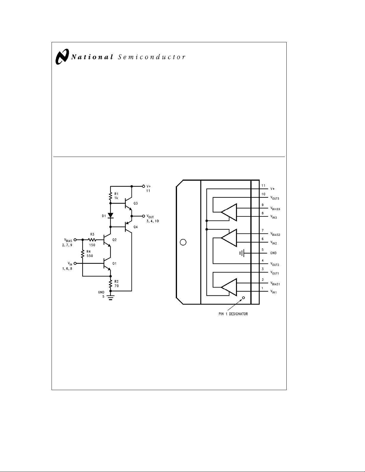
Schematic and Connection Diagrams
One Channel
Features
Y
50 VPPoutput swing at 65 MHz
Y
Rise/Fall time 5 ns with 12 pF load
Y
60 VPPoutput swing capability
Y
Pin and function compatible with LM2416
Y
No low frequency tilt compensation required
Applications
Y
CRT driver for SVGA, IBM 8514 and 1024 x 768
display resolution RGB monitors
TL/H/11442– 1
Order Number LM2419T
See NS Package Number TA11B
C
1995 National Semiconductor Corporation RRD-B30M115/Printed in U. S. A.
TL/H/11442
TL/H/11442– 2
Page 2

Absolute Maximum Ratings (Note 1)
If Military/Aerospace specified devices are required,
please contact the National Semiconductor Sales
Office/Distributors for availability and specifications.
Supply Voltage (V
Storage Temperature (T
Operating Case Temperature, T
Lead Temperature (solderingk10 sec.) 300§C
ESD Tolerance 2 kV
a
)
)
STG
Case
b
25§Ctoa100§C
b
a
85V
20§Ctoa90§C
Electrical Characteristics
Unless otherwise specified, the following specifications apply for V
swing; frequency
Symbol Parameter Conditions
I
CC
I
B
V
OUT
t
r
t
f
A
V
OS Overshoot VIN:tr,t
LE Linearlty Error V
e
1 MHz; V
Bias
e
12V; C
L
e
12 pF; T
A
Supply Current (per Amplifier) Input/Output Open Circuit 27 40 mA
Bias Current (Pins 2 or 7 or 9) 11 mA
Output Offset Voltage 40 50 60 V
Rise Time 10% to 90% 5 ns
Fall Time 90% to 10% 5 ns
Voltage Gain
k
f
e
25V to 75V 8 %
OUT
a
e
e
25§C; see test circuit,
80V, DC input bias, V
Figure 1
.
IN DC
e
3.9V; 50 VPPoutput
Min Typ Max Units
(Note 3) (Note 2) (Note 3) (Limit)
b
13
b
15
b
18 V/V
2ns 8 %
DAVmatch Gain Matching 0.3 dB
Note 1: Absolute Maximum Ratings indicate limits beyond which damage to the device may occur. The guaranteed specifications apply only for the test conditions
listed. Some performance characteristics may degrade when the device is not operated under the listed test conditions.
Note 2: Typical specifications are at 25
Note 3: Min/Max limits are guaranteed to National’s AOQL (Average Outgoing Quality Level).
C and represent the most likely parametric norm.
§
Typical Performance
Characteristics
e
T
25§C, Test CircuitÐ
A
Figure 1
Frequency Response
*12 pF is the total load capacitance and includes the test fixture capacitance.
TL/H/11442– 3
FIGURE 1. Test Circuit (One Section)
TL/H/11442– 4
2
Page 3

Typical Performance
Characteristics
e
T
25§C, Test CircuitÐ
A
Pulse Response
(Continued)
Figure 1
small signal cross over distortion. Resistor R3 is used to
prevent Q2 from oscillating at high frequencies.
TL/H/11442– 5
Test Circuit
Figure 1
LM2419. The input signal is AC coupled into the input of
LM2419 and is referenced to 3.9V DC using an external
3.9V DC bias through a 390X resistor. The test circuit is
designed to allow testing of the LM2419 in a 50X environment such as a 50X oscilloscope or network analyzer. The
4950X resistor in series with the output of the LM2419
forms a 100:1 voltage divider when connected to a 50X
oscilloscope or network analyzer.
shows a typical test circuit for evaluation of the
Theory of Operation
The LM2419 is a high voltage triple CRT driver suitable for
SVGA, IBM 8514 and 1024 x 768 display resolution monitors. The device is packaged in the industry standard
11 lead TO-220 molded power package. The heat sink is
electrically isolated and may be grounded for ease of manufacturing and RFl/EMl shielding.
The schematic diagram of LM2419 is shown in
and R2 provide a conversion of the input voltage to current
while Q2 acts as a common base amplifier to drive the load
resistor, R1. Resistor R4 along with R2 sets up the DC bias
at the base of Q1. Emitter followers Q3 and Q4 isolate R1
from the capacitive load at the output, thus making the rise
and fall times relatively insensitive to the load capacitance.
The gain of the amplifier is
approximately
limited by the time constant due to R1 and the capacitances
associated with D1, Q2, Q3 and Q4. Diode D1 is used to
provide some bias voltage for Q3 and Q4 so as to reduce
b
15. The bandwidth of LM2419 is primarily
b
R1/(R2llR4) and is fixed at
Figure 2
.Q1
FIGURE 2. Schematic Diagram of
One Section of LM2419
TL/H/11442– 7
Application Hints
POWER SUPPLY BYPASS
Since the LM2419 is a wide-bandwidth amplifier with greater
than 10,000 V/ms slew rate, proper power supply bypassing
is critical for optimum performance. Improper power supply
bypassing can result in large overshoot, ringing and oscillation. A 0.01 mF ceramic capacitor should be connected as
close to the supply pin as is practical (preferably less than
(/4
from the supply pin). The lead length of the 0.01 mF
×
ceramic capacitor should be as small as is practical. In addition, 10 mF–100 mF electrolytic capacitor should be connected from the supply pin to ground. The electrolytic capacitor should be placed reasonably close to the LM2419’s
supply pin.
ARC PROTECTION
The LM2419 must be protected from arcing within the CRT.
To limit the arcover voltage, a 200V spark gap is recommended at the cathode. Clamp diodes D1 and D2 (as
shown in
output of LM2419 to a safe level. The clamp diodes used
should have high current rating, low series impedance and
low shunt capacitance. Resistor R2 in
arcover current while R1 limits the current into LM2419 and
reduces the power dissipation of the output transistors
when the output is stressed beyond the supply voltage.
Having large value resistors for R1 and R2 would be desirable but this has the effect of reducing rise and fall times.
Figure 3
) are used to clamp the voltage at the
Figure 3
limits the
3
Page 4

Application Hints (Continued)
FIGURE 3. Typical Application Circuit (One Channel)
IMPROVING RISE AND FALL TIMES
Because of an emitter follower output stage, the rise and fall
times of the LM2419 are relatively unaffected by capacitive
loading. However, the series resistors R1 and R2 (see
ure 3
) will reduce the rise and fall times when driving the
Fig-
CRT’s cathode which appears as a capacitive load. The capacitance at the cathode typically ranges from 8 pF to
12 pF.
To improve the rise and fall times at the cathode, a small
inductor is often used in series with the output of the amplifier. The inductor L1 in
Figure 3
peaks the amplifier’s frequency response at the cathode, thus improving rise and fall
times. The inductor value is empirically determined and is
dependent on the load. An inductor value of 0.1 mHisa
good starting value. Note that peaking the amplifier’s frequency response will increase the overshoot.
REDUCING OVERSHOOT
LM2419’s overshoot is a function of both the input signal
rise and fall times and the capacitive loading. The overshoot
is increased by either more capacitive loading or faster rise
and fall times of the input signal.
Table I shows the overshoot for a typical device with different capacitive loads and different input signal rise and fall
times. As can be observed from Table I, overshoot is large
for large capacitive loads and faster input signal rise and fall
times. In an actual application, the LM2419 is driven from a
preamplifier with rise and fall times of 3 ns to 7 ns. When
driven from LM1203 preamplifier (see application circuit,
Figure 6
) the overshoot is 10% with 12 pF capacitive load.
The overshoot can be reduced by including a resistor in
series with LM2419’s output as in
Figure 3
. Larger value
resistors for R1 and R2 would reduce overshoot but this
also increases the rise and fall times at the output. Frequency peaking using an inductor in series with the output may
restore the bandwidth.
TL/H/11442– 8
Table I. LM2419 Output Overshoot
vs Capacitive Loading for a Typical Device
Input Signal C
tr/t
f
5 pF 8 pF 11 pF 15 pF
L
1.2 ns 4% 6% 7% 8%
7ns 4% 5% 6% 7%
GAIN VS OUTPUT DC LEVEL
Figure 4
Figure 4
shows LM2419’s gain versus output DC level. A
100 mV
the input signal’s DC level is swept. As can be seen from
15.4 (V
and 65V. Thus the amplifier’s output response is linear for
AC signal is applied at the LM2419’s input and
PP
, the amplifier’s gain is constant at approximately
e
1.54 VPP) for output DC level between 35V
OUT
output voltage between 35V and 65V. If the output voltage
is less than 35V or more than 70V, the amplifier’s output
response becomes non-linear (note the change in gain,
ure 4
). For optimum performance, it is recommended that
Fig-
LM2419’s output low voltage be at 25V or above. For a
50 V
swing, the output high voltage is 75V. With an output
PP
signal swing from 25V to 75V, LM2419’s linearity error is
measured at 8%.
TL/H/11442– 9
FIGURE 4. Gain vs V
OUT
(DC), V
e
100 mV
IN
PP
4
Page 5

Application Hints (Continued)
THERMAL CONSIDERATIONS
LM2419’s transfer characteristic and power dissipation versus DC input voltage is shown in
current increases as the input voltage increases, consequently power dissipation increases. For the LM2419, the
worst case power dissipation occurs when a white screen is
displayed on the CRT. Considering a 20% black retrace
time in a 1024 x 768 display resolution application, the average power dissipation for continuous white screen is less
than 4W per channel with 50 V
at 75V and white level at 25V). Although the total power
dissipation is less than 12W for a continuous white screen,
the heat sink should be selected for 13W power dissipation
because of the variation in power dissipation from part to
part.
For thermal and gain linearity considerations, the output low
voltage (white level) should be maintained above 20V. If the
device is operated at an output low voltage below 20V, the
power dissipation might exceed 4.7W per channel (i.e., 14W
power dissipation for the device). Note that the device can
be operated at lower power by reducing the peak to peak
video output voltage to less than 50V and clamping the video black level close to the supply voltage.
FIGURE 5. V
and Power Dissipation vs V
OUT
Figure 5
. Power supply
output signal (black level
PP
TL/H/11442– 10
IN
The LM2419 requires that the package be properly heat
sunk under all operating conditions. Maximum ratings re-
quire that the device case temperature be limited to 90
maximum. Thus for 50
and 13W maximum power dissipation, the thermal resistance of the heat sink should be:
i
sa
SHORT CIRCUIT PROTECTION
The output of LM2419 is not short circuit protected. Shorting the output to either ground or to V
device. The minimum DC load resistance the LM2419 can
drive without damage is 1.6 kX to ground or V
driving a 1.6 kX load for an extended period of time is not
recommended because of power dissipation considerations. If the LM2419 is used to drive a resistive load then the
load should be 10 kX or greater.
C maximum ambient temperature
§
s
(90–50)§C/13We3§C/W
a
will destroy the
a
. However,
RGB Video Application
A complete video section for an RGB CRT monitor is shown
in
Figure 6
include almost all the circuitry required between the video
input connection and the CRT’s cathodes. However, an externally generated back porch clamp signal is required to
accomplish DC restoration of the video signal.
Figure 6
1024 x 768 display resolution application. With 50 V
put swing and 12 pF load, the rise/fall time for
circuit was measured at 7.5 ns. In this application, feedback
is local to the LM1203. For detailed information on the
LM1203, please refer to the LM1203 data sheet.
PC BOARD LAYOUT CONSIDERATIONS
For optimum performance, adequate ground plane, isolation
between channels, good supply bypassing and minimizing
unwanted feedback are necessary. Moreover, the length of
the signal trace from the preamplifier to the LM2419 and
from the LM2419 to the cathode should be as short as is
practical. The following book is highly recommended:
Ott, Henry W,
Systems
. The LM1203 video preamplifier and the LM2419
’s circuit is excellent choice for a non-interlaced
PP
Figure 6
out-
Noise Reduction Techniques in Electronic
, John Wiley & Sons, New York, 1976.
C
§
’s
5
Page 6

Application Hints (Continued)
FIGURE 6. Typical VGA/SVGA Application
6
TL/H/11442– 11
Page 7

Application Hints (Continued)
TL/H/11442– 12
FIGURE 7. Typical SVGA/XGA Application
Diodes FDH400
Unmarked capacitors 0.1 mF
7
Page 8

Physical Dimensions inches (millimeters) Lit.
LM2419 Triple 65 MHz CRT Driver
Order Number LM2419T
NS Package Number TA11B
Ý
107763
LIFE SUPPORT POLICY
NATIONAL’S PRODUCTS ARE NOT AUTHORIZED FOR USE AS CRITICAL COMPONENTS IN LIFE SUPPORT
DEVICES OR SYSTEMS WITHOUT THE EXPRESS WRITTEN APPROVAL OF THE PRESIDENT OF NATIONAL
SEMICONDUCTOR CORPORATION. As used herein:
1. Life support devices or systems are devices or 2. A critical component is any component of a life
systems which, (a) are intended for surgical implant support device or system whose failure to perform can
into the body, or (b) support or sustain life, and whose be reasonably expected to cause the failure of the life
failure to perform, when properly used in accordance support device or system, or to affect its safety or
with instructions for use provided in the labeling, can effectiveness.
be reasonably expected to result in a significant injury
to the user.
National Semiconductor National Semiconductor National Semiconductor National Semiconductor
Corporation Europe Hong Kong Ltd. Japan Ltd.
1111 West Bardin Road Fax: (
Arlington, TX 76017 Email: cnjwge@tevm2.nsc.com Ocean Centre, 5 Canton Rd. Fax: 81-043-299-2408
Tel: 1(800) 272-9959 Deutsch Tel: (
Fax: 1(800) 737-7018 English Tel: (
National does not assume any responsibility for use of any circuitry described, no circuit patent licenses are implied and National reserves the right at any time without notice to change said circuitry and specifications.
Fran3ais Tel: (
Italiano Tel: (
a
49) 0-180-530 85 86 13th Floor, Straight Block, Tel: 81-043-299-2309
a
49) 0-180-530 85 85 Tsimshatsui, Kowloon
a
49) 0-180-532 78 32 Hong Kong
a
49) 0-180-532 93 58 Tel: (852) 2737-1600
a
49) 0-180-534 16 80 Fax: (852) 2736-9960
 Loading...