

Page 1
LM2405
Monolithic Triple 7 ns CRT Driver
General Description
The LM2405 is an integrated high voltage CRT driver circuit
designed for use in color monitor applications. The IC contains three high input impedance, wide band amplifiers
which directly drivethe RGB cathodes of a CRT. Each channel has its gain internally set at −14 and can drive CRT capacitive loads as well as resistive loads presented by other
applications, limited only by the package’s power dissipation.
The IC is packaged in an industry standard 11 lead TO-220
molded plastic power package. See thermal considerations
on page 5.
Features
n Rise/fall times typically 7 ns with 8 pF load
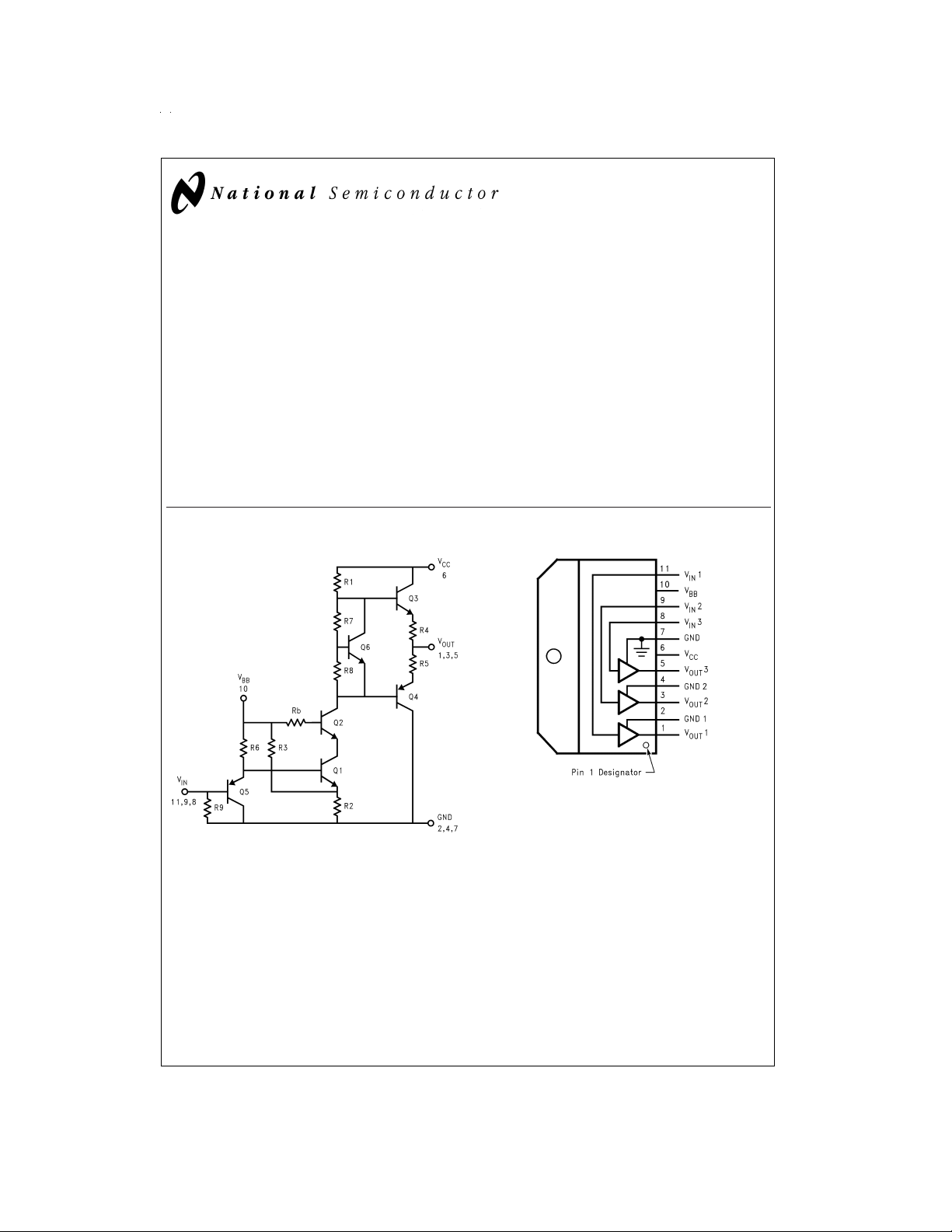
Schematic and Connection Diagram
n Output swing capability:
50 V
40 V
30 V
n Pinout designed for easy PCB layout
n 0V to 6V input range
n Stable with 0 pF–20 pF capactive loads
n Convenient TO-220 staggered lead package style
Applications
n CRT driver for 1280 x 1024 (Non-interlaced) and XGA
display resolution color monitors
n Pixel clock frequency up to 130 MHz
n Monitors using video blanking
LM2405 Monolithic Triple 7 ns CRT Driver
August 1999
=
for V
PP
for V
PP
for V
PP
80
CC
=
70
CC
=
60
CC
TabisatGND
Top View
DS012682-1
FIGURE 1. Simplified Schematic Diagram (One
Channel)
© 1999 National Semiconductor Corporation DS012682 www.national.com
Order Number LM2405T
DS012682-2
Page 2
Absolute Maximum Ratings (Notes 1, 3)
Supply Voltage (V
Bias Voltage (V
Input Voltage (V
Storage Temperature Range
) −65˚C to +150˚C
(T
STG
Lead Temperature
(Soldering,
) +90V
CC
) +16V
BB
) −0.5V to V
IN
<
10 sec.) 300˚C
BIAS
+ 0.5V
Operating Ranges (Note 2)
V
CC
V
BB
V
IN
Case Temperature (T
Do not operate the part without a heat sink.
) −20˚C to +100˚C
CASE
+60V to +85V
+8V to +15V
0V to +6V
ESD Tolerance 2 kV
Electrical Characteristics
Unless otherwise noted: V
=
T
25˚C.
A
CC
=
+80V, V
Symbol Parameter Conditions
I
I
V
A
∆A
CC
BB
OUT
V
V
Supply Current Per Channel, No Output Load 18 30 mA
Bias Current 38 mA
DC Output Voltage No Input Signal 47 50 53 V
DC Voltage Gain No Input Signal −12 −14 −16
Gain Matching No Input Signal (Note 4) 1.0 dB
LE Linearity Error No Input Signal (Notes 4, 5) 8
t
R
t
F
Note 1: Absolute Maximum Ratings indicate limits beyond which damage to the device may occur.
Note 2: Operating ratings indicate conditions for which the device is functional, but do not guarantee specific performance limits. For guaranteed specifications and
test conditions, see the Electrical Characteristics. The guaranteed specifications apply only for the test conditions listed. Some performance characteristics may
change when the device is not operated under the listed test conditions.
Note 3: All voltages are measured with respect to GND, unless otherwise specified.
Note 4: Calculated value from Voltage Gain test on each channel.
Note 5: Linearity Error is the variation in DC gain from V
Note 6: Input from signal generator: t
Rise Time 10%to 90
Fall Time 90%to 10
R,tF
=
+12V, V
BB
1 ns.
IN
<
%
%
=
+ 1.3V to V
=
+2.6V (at LM2405 input pins), C
IN
Min Typical Max
=
+3.9V.
IN
=
8 pF, Output=40 V
L
LM2405
at 1 MHz,
PP
Units
7ns
5.5 ns
DC
%
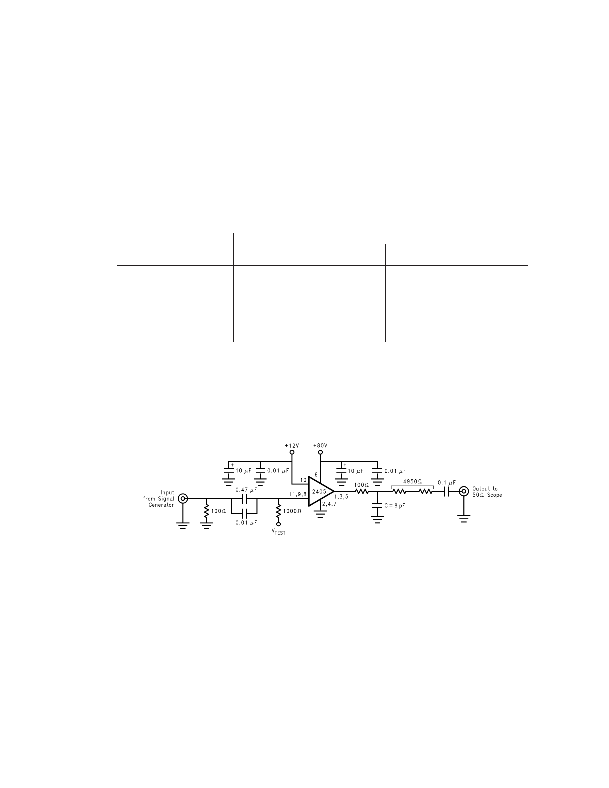
AC Test Circuit
Note: 8 pF is total load plus parasitic capacitance.
Note: Adjust Vtest for +2.6V DC at LM2405 input pins. See “Input Resistance” section of Application Hints.
FIGURE 2. Test Circuit (One Channel)
Figure 2
LM2405. This circuit is designed to allow testing of the
LM2405 in a 50Ω environment, such as a pulse generator,
oscilloscope or network analyzer. The 4950Ω resistor at the
output forms a 100:1 voltage divider when connected to a
50Ω load.
www.national.com 2
shows a typical test circuit for evaluation of the
DS012682-3
Page 3
AC Test Circuit (Continued)
DS012682-7
FIGURE 6. Pulse Response
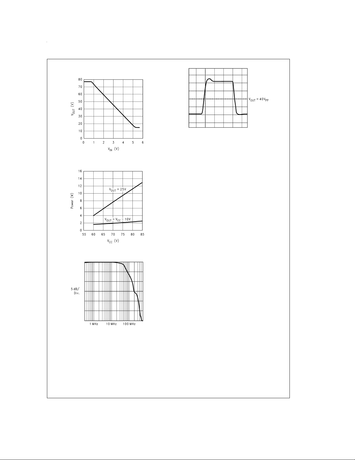
DS012682-4
FIGURE 3. V
FIGURE 4. Power Dissipation vs V
OUT
vs V
IN
DS012682-5
CC
DS012682-6
FIGURE 5. Large Signal Frequency Response
Theory of Operation
The LM2405 is a high voltage monolithic triple CRT driver
suitable for SVGA and XGA display applications. The
LM2405 features +80V operation and low power dissipation.
The part is housed in the industry standard 11-lead TO-220
molded plastic power package.
The circuit diagram of the LM2405 is shown in
Figure 1
.A
PNP emitter follower, Q5, provides input buffering. Q1 and
Q2 form a fixed gain cascode amplifier, with a gain of −14.
Emitter followers Q3 and Q4 isolate the high output impedance of the amplifier from the capacitance of the CRT cathode, and make the circuit relative insensitive to load capacitance. Q6 provides biasing to the output emitter follower
stage to reduce crossover distortion at low signal levels.
Figure 2
shows a typical test circuit for evaluation of the
LM2405. This circuit is designed to allow testing of the
LM2405 in a 50Ω environment, such as a pulse generator
and a scope, or a network analyzer. In this test circuit, two
low inductance resistors in series totaling 4.95 kΩ form a
100:1 wideband low capacitance probe when connected to a
50Ω cable and load. The input signal from the generator is
AC coupled to the base of Q5.
Application Hints
INTRODUCTION
National Semiconductor is committed to providing application information that assists our customers in obtaining the
best performance possible from our products. The following
information is provided in order to support this commitment.
The reader should be aware that the optimization of performance was done using a specific printed circuit board designed at National. Variations in performance can be realized
due to physical changes in the printed circuit board and the
application. Therefore, the designer should be aware that
component value changes may be required in order to optimize performance in a given application. The values shown
in this document can be used as a starting point for evaluation purposes. When working with high bandwidth circuits,
good layout practices are also critical to achieving maximum
performance.
POWER SUPPLY BYPASS
Since the LM2405 is a wide bandwidth amplifier, proper
power supply bypassing is critical for optimum performance.
Improper power supply bypassing can result in large overshoot, ringing and oscillation. A 0.01 µF capacitor should be
connected from the supply pin, V
, to ground, as close to
CC
www.national.com3
Page 4

Application Hints (Continued)
the supply pin as is practical (preferably less than
the supply pin). Additionally, a 10 µF to 100 µF electrolytic
capacitor should be connected from the supply pin to
ground. The electrolytic capacitor should also be placed reasonably close to the LM2405’s supply pin. A 0.1 µF capacitor
should be connected from the bias pin, V
close as is practical to the part.
ARC PROTECTION
During normal CRT operation, internal arcing may occasionally occur. Spark gaps of 200V to 300V at the cathodes will
limit the maximum voltage, but to a value that is much higher
than allowable on the LM2405. This fast, high voltage, high
energy pulse can damage the LM2405 output stage. The addition of clamp diodes D1 and D2 (as shown in
help clamp the voltage at the output of the LM2405 to a safe
level. The clamp diodes should have a fast transient response, high peak current rating, low series impedance and
low shunt capacitance. FDH400 or equivalent diodes are
recommended. Resistor R2 in
Figure 7
current while R1 limits the current into the LM2405 and reduces the power dissipation of the output transistors when
the output is stressed beyond the supply voltage. (Peaking
inductor Lp also helps protect the CRT driver from arc over.)
Having large value resistors for R1 and R2 would be desirable, but this has the effect of increasing rise and fall times.
For proper arc protection, it is important to not omit any of the
arc protection components shown in
Figure 7
FIGURE 7. One Section of the LM2405 with Arc
Protection and Peaking Inductor L
There are also ESD protection diodes built into the part. To
avoid damaging these diodes, do not apply an input voltage
from a low impedance source when the V
are held at ground potential.
IMPROVING RISE AND FALL TIMES
Because of an emitter follower output stage, the rise and fall
times of the LM2405 are relatively insensitive to capactive
loading. However, the series resistors R1 and R2 (see
ure 7
) will increase the rise and fall times when driving the
CRT’s cathode which appears as a capacitive load. The capacitance at the cathode typically ranges from 8 pF to 12 pF.
To improve the rise and fall times at the cathode, a small inductor is often used in series with the output of the amplifier.
The inductor L
response at the cathode, thus improving rise and fall times.
P
in
Figure 7
peaks the amplifier’s frequency
It also acts with the output load capacitance to form a low
pass filter, which reduces the amplitudes of high frequency
harmonics of the video signal, to lower radiated electromagnetic interference. The inductor value is empirically determined and is dependent on the load. An inductor value of
0.22 µH is a good starting value. Note that excessive peak-
1
⁄4" from
, to ground, as
BB
Figure 7
) will
limits the arcover
.
DS012682-8
P
and VCCpins
BB
Fig-
ing of the amplifier’s frequency response will increase the
overshoot. (Increasing the value of resistor R1 or R2 will reduce ringing and overshoot.)
EFFECT OF LOAD CAPACITANCE
The output rise and fall times will be slower than specified if
the load capacitance at the output is more than 8 pF, as
shown in
Figure 8
.
DS012682-9
FIGURE 8. Effect of Load Capacitance on
Rise/Fall Time
The monitor designer should ensure that stray capacitance
applied to the LM2405 is as low as possible.
THERMAL CONSIDERATIONS
Power supply current increases as the input signal increases
and consequently power dissipation also increases.
The LM2405 cannot be used without heat sinking. Typical
“average” power dissipation with the device output voltage at
one half the supply voltage is 2.4W per channel for a total
dissipation of 7.2W package dissipation. Under white screen
conditions, i.e., 25V output, dissipation increases to 3.5W
per channel or 10.5W total. The LM2405 case temperature
must be maintained below 100˚C. If the maximum expected
ambient temperature is 50˚C, then a maximum heat sink
thermal resistance can be calculated:
This example assumes a typical CRT capacitive load and is
without a resistive load. Note that this thermal resistance
must be achieved when the heat sink is operating in the
monitor.
INPUT RESISTANCE
The LM2405 has a fixed resistor of 3000Ω connected from
each signal input pin to ground. In the
Figure 2
Test Circuit,
the input DC voltage level, Vtest, must be adjusted, (to about
+3.5V) to allow for the voltage drop across the 1000Ω resistor, to set the actual voltage at the input pins to +2.6V. In actual use in a monitor, the 1000Ω resistor is not used and the
video preamp supplies the 2.6V offset.
PC BOARD LAYOUT CONSIDERATIONS
For optimum performance, an adequate ground plane, isolation between channels, good supply bypassing and minimizing unwanted feedback are necessary.Also,the length of the
www.national.com 4
Page 5

Application Hints (Continued)
signal traces from the preamplifier to the LM2405 and from
the LM2405 to the CRT cathode should be as short as possible. The following references are recommended:
Ott, Henry W., “Noise Reduction Techniques in Electronic
Systems”, John Wiley and Sons, New York, 1976.
“Guide to CRT Video Design”, National Semiconductor Application Note 861.
“Video Amplifier Design for Computer Monitors”, National
Semiconductor Application Note 1013.
Because of its high small signal bandwidth, the part may oscillate when it is used in a typical application with a preamp
in a monitor, if feedback occurs around the video amplifier
through the chassis wiring. To prevent this, leads to the input
circuit should be shielded, and input circuit wiring should be
spaced as far as possible from output circuit wiring. Power
should be removed as quickly as possible from an amplifier
that is oscillating, since power dissipation in the part is very
high in this mode and the part may be damaged if oscillations continue and the power supply can supply more than
250 mA.
TYPICAL APPLICATION
A typical application of the LM2405 is shown in
Used in conjunction with an LM1205, a complete video channel from monitor input to CRTcathode can be achieved. Performance is satisfactory for all applications up to 1280x1024
non-interlaced, and pixel clock frequencies up to 130 MHz.
Figure 9
.
www.national.com5
Page 6

Application Hints (Continued)
DS012682-10
www.national.com 6
Diodes FDH400
PNP Transistors MPSA92
NPN Transistors 2N2369
Unmarked Capacitors 0.1 µF
FIGURE 9. Typical Application
Page 7

Physical Dimensions inches (millimeters) unless otherwise noted
LM2405
11-Lead Molded TO-220
NS Package Number TA11B
Order Number LM2405T
LM2405 Monolithic Triple 7 ns CRT Driver
LIFE SUPPORT POLICY
NATIONAL’S PRODUCTS ARE NOT AUTHORIZED FOR USE AS CRITICAL COMPONENTS IN LIFE SUPPORT
DEVICES OR SYSTEMS WITHOUT THE EXPRESS WRITTEN APPROVAL OF THE PRESIDENT AND GENERAL
COUNSEL OF NATIONAL SEMICONDUCTOR CORPORATION. As used herein:
1. Life support devices or systems are devices or
systems which, (a) are intended for surgical implant
into the body, or (b) support or sustain life, and
whose failure to perform when properly used in
accordance with instructions for use provided in the
2. A critical component is any component of a life
support device or system whose failure to perform
can be reasonably expected to cause the failure of
the life support device or system, or to affect its
safety or effectiveness.
labeling, can be reasonably expected to result in a
significant injury to the user.
National Semiconductor
Corporation
Americas
Tel: 1-800-272-9959
Fax: 1-800-737-7018
Email: support@nsc.com
www.national.com
National does not assume any responsibility for use of any circuitry described, no circuit patent licenses are implied and National reserves the right at any time without notice to change said circuitry and specifications.
National Semiconductor
Europe
Fax: +49 (0) 1 80-530 85 86
Email: europe.support@nsc.com
Deutsch Tel: +49 (0) 1 80-530 85 85
English Tel: +49 (0) 1 80-532 78 32
Français Tel: +49 (0) 1 80-532 93 58
Italiano Tel: +49 (0) 1 80-534 16 80
National Semiconductor
Asia Pacific Customer
Response Group
Tel: 65-2544466
Fax: 65-2504466
Email: sea.support@nsc.com
National Semiconductor
Japan Ltd.
Tel: 81-3-5639-7560
Fax: 81-3-5639-7507
 Loading...