Page 1

LM231A/LM231/LM331A/LM331
Precision Voltage-to-Frequency Converters
General Description
The LM231/LM331 family of voltage-to-frequency converters
are ideally suited for use in simple low-cost circuits for
analog-to-digital conversion, precision frequency-to-voltage
conversion, long-term integration, linear frequency modulation or demodulation, and many other functions. The output
when used as a voltage-to-frequency converter is a pulse
train at a frequency precisely proportional to the applied input voltage. Thus, it provides all the inherent advantages of
the voltage-to-frequency conversion techniques, and is easy
to apply in all standard voltage-to-frequency converter applications. Further, the LM231A/LM331A attain a new high
level of accuracy versus temperature which could only be attained with expensive voltage-to-frequency modules. Additionally the LM231/331 are ideally suited for use in digital
systems at low power supply voltages and can provide
low-cost analog-to-digital conversion in
microprocessor-controlled systems. And, the frequency from
a battery powered voltage-to-frequency converter can be
easily channeled through a simple photoisolator to provide
isolation against high common mode levels.
The LM231/LM331 utilize a new temperature-compensated
band-gap reference circuit, to provide excellent accuracy
over the full operating temperature range, at power supplies
as low as 4.0V. The precision timer circuit has low bias currents without degrading the quick response necessary for
100 kHz voltage-to-frequency conversion. And the output
are capable of driving 3 TTL loads, or a high voltage output
up to 40V, yet is short-circuit-proof against V
CC
.
Features
n Guaranteed linearity 0.01%max
n Improved performance in existing voltage-to-frequency
conversion applications
n Split or single supply operation
n Operates on single 5V supply
n Pulse output compatible with all logic forms
n Excellent temperature stability,
±
50 ppm/˚C max
n Low power dissipation, 15 mW typical at 5V
n Wide dynamic range, 100 dB min at 10 kHz full scale
frequency
n Wide range of full scale frequency, 1 Hz to 100 kHz
n Low cost
Typical Applications
Teflon®is a registered trademark of DuPont
DS005680-1
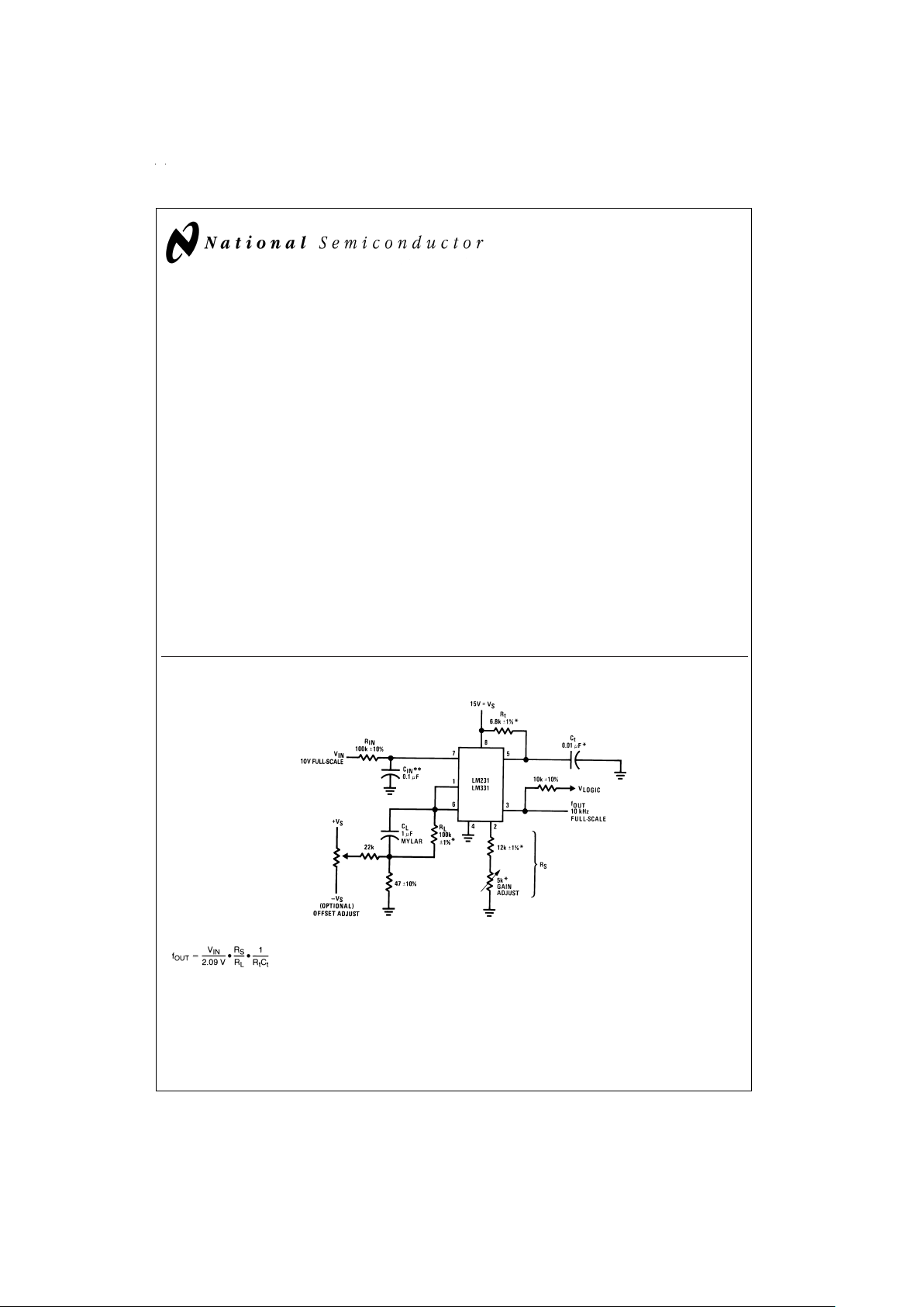
*
Use stable components with low temperature coefficients. See Typical Applications section.
**
0.1µF or 1µF, See “Principles of Operation.”
FIGURE 1. Simple Stand-Alone Voltage-to-Frequency Converter
with
±
0.03%Typical Linearity (f=10 Hz to 11 kHz)
June 1999
LM231A/LM231/LM331A/LM331 Precision Voltage-to-Frequency Converters
© 1999 National Semiconductor Corporation DS005680 www.national.com
Page 2

Absolute Maximum Ratings (Note 1)
If Military/Aerospace specified devices are required, please contact the National Semiconductor Sales Office/
Distributors for availability and specifications.
LM231A/LM231 LM331A/LM331
Supply Voltage 40V 40V
Output Short Circuit to Ground Continuous Continuous
Output Short Circuit to V
CC
Continuous Continuous
Input Voltage −0.2V to +V
S
−0.2V to +V
S
T
MINTMAX
T
MINTMAX
Operating Ambient Temperature Range −25˚C to +85˚C 0˚C to +70˚C
Power Dissipation (P
D
at 25˚C)
and Thermal Resistance (θ
jA
)
(N Package) P
D
1.25W 1.25W
θ
jA
100˚C/W 100˚C/W
Lead Temperature (Soldering, 10 sec.)
Dual-In-Line Package (Plastic) 260˚C 260˚C
ESD Susceptibility (Note 4)
N Package 500V 500V
Electrical Characteristics
T
A
=
25˚C unless otherwise specified (Note 2)
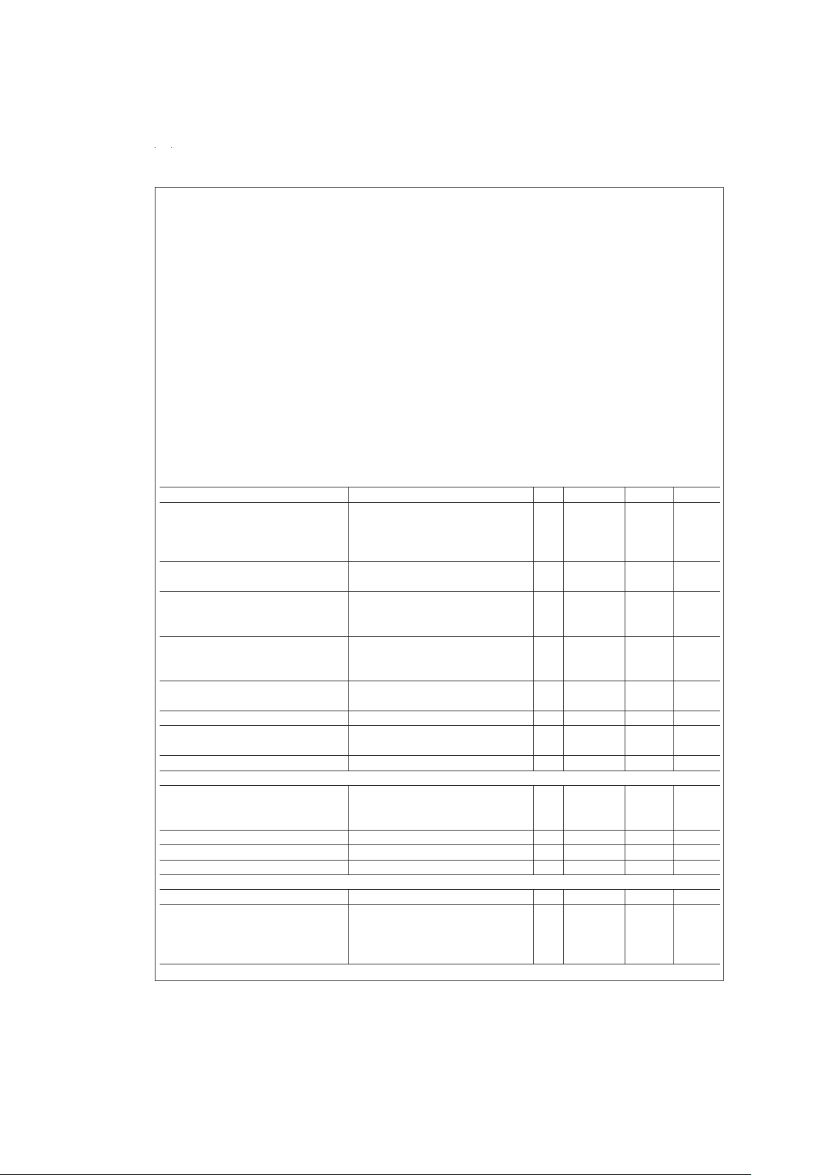
Parameter Conditions Min Typ Max Units
VFC Non-Linearity (Note 3) 4.5V ≤ V
S
≤ 20V
±
0.003
±
0.01
%
Full-
Scale
T
MIN
≤ TA≤ T
MAX
±
0.006
±
0.02
%
Full-
Scale
VFC Non-Linearity V
S
=
15V, f=10 Hz to 11 kHz
±
0.024
±
0.14
%
Full-
In Circuit of
Figure 1
Scale
Conversion Accuracy Scale Factor (Gain) V
IN
=
−10V, R
S
=
14 kΩ
LM231, LM231A 0.95 1.00 1.05 kHz/V
LM331, LM331A 0.90 1.00 1.10 kHz/V
Temperature Stability of Gain T
MIN
≤ TA≤ T
MAX
, 4.5V ≤ VS≤ 20V
LM231/LM331
±
30
±
150 ppm/˚C
LM231A/LM331A
±
20
±
50 ppm/˚C
Change of Gain with V
S
4.5V ≤ VS≤ 10V 0.01 0.1
%
/V
10V ≤ V
S
≤ 40V 0.006 0.06
%
/V
Rated Full-Scale Frequency V
IN
=
−10V 10.0 kHz
Gain Stability vs Time T
MIN
≤ TA≤ T
MAX
±
0.02
%
Full-
(1000 Hrs) Scale
Overrange (Beyond Full-Scale) Frequency V
IN
=
−11V 10
%
INPUT COMPARATOR
Offset Voltage
±
3
±
10 mV
LM231/LM331 T
MIN
≤ TA≤ T
MAX
±
4
±
14 mV
LM231A/LM331A T
MIN
≤ TA≤ T
MAX
±
3
±
10 mV
Bias Current −80 −300 nA
Offset Current
±
8
±
100 nA
Common-Mode Range T
MIN
≤ TA≤ T
MAX
−0.2 VCC−2.0 V
TIMER
Timer Threshold Voltage, Pin 5 0.63 0.667 0.70 x V
S
Input Bias Current, Pin 5 V
S
=
15V
All Devices 0V ≤ V
PIN 5
≤ 9.9V
±
10
±
100 nA
LM231/LM331 V
PIN 5
=
10V 200 1000 nA
LM231A/LM331A V
PIN 5
=
10V 200 500 nA
www.national.com 2
Page 3

Electrical Characteristics (Continued)
T
A
=
25˚C unless otherwise specified (Note 2)
Parameter Conditions Min Typ Max Units
TIMER
V
SAT PIN 5
(Reset) I=5 mA 0.22 0.5 V
CURRENT SOURCE (Pin 1)
Output Current R
S
=
14 kΩ,V
PIN 1
=
0
LM231, LM231A 126 135 144 µA
LM331, LM331A 116 136 156 µA
Change with Voltage 0V ≤ V
PIN 1
≤ 10V 0.2 1.0 µA
Current Source OFF Leakage
LM231, LM231A, LM331, LM331A 0.02 10.0 nA
All Devices T
A
=
T
MAX
2.0 50.0 nA
Operating Range of Current (Typical) (10 to 500) µA
REFERENCE VOLTAGE (Pin 2)
LM231, LM231A 1.76 1.89 2.02 V
DC
LM331, LM331A 1.70 1.89 2.08 V
DC
Stability vs Temperature
±
60 ppm/˚C
Stability vs Time, 1000 Hours
±
0.1
%
LOGIC OUTPUT (Pin 3)
V
SAT
I=5 mA 0.15 0.50 V
I=3.2 mA (2 TTL Loads), T
MIN≤TA≤TMAX
0.10 0.40 V
OFF Leakage
±
0.05 1.0 µA
SUPPLY CURRENT
LM231, LM231A V
S
=
5V 2.0 3.0 4.0 mA
LM331, LM331A V
S
=
40V 2.5 4.0 6.0 mA
V
S
=
5V 1.5 3.0 6.0 mA
V
S
=
40V 2.0 4.0 8.0 mA
Note 1: Absolute Maximum Ratings indicate limits beyond which damage to the device may occur. DC and AC electrical specifications do not apply when operating
the device beyond its specified operating conditions.
Note 2: All specifications apply in the circuit of
Figure 4
, with 4.0V≤VS≤40V, unless otherwise noted.
Note 3: Nonlinearity is defined as the deviation of f
OUT
from VINx (10 kHz/−10 VDC) when the circuit has been trimmed for zero error at 10 Hz and at 10 kHz, over
the frequency range 1 Hz to 11 kHz. For the timing capacitor, C
T
, use NPO ceramic, Teflon®, or polystyrene.
Note 4: Human body model, 100 pF discharged through a 1.5 kΩ resistor.
www.national.com3
Page 4

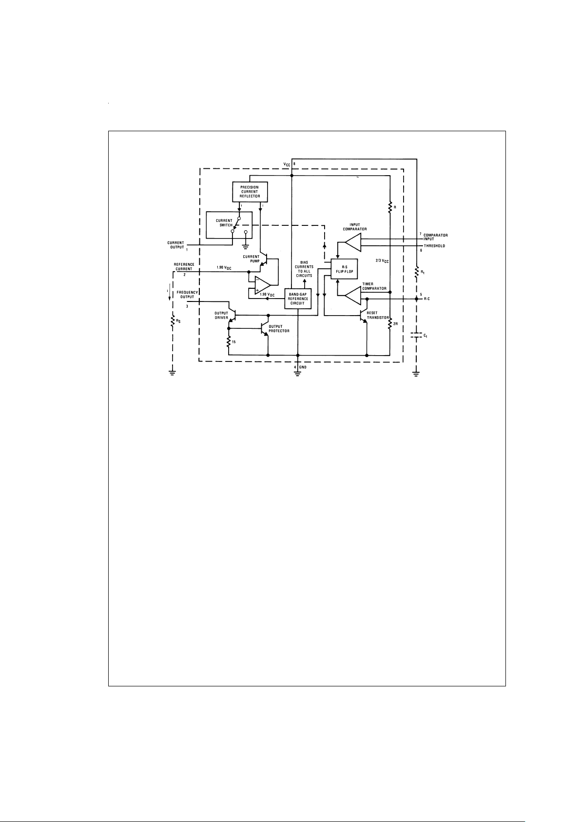
Functional Block Diagram
DS005680-2
Pin numbers apply to 8-pin packages only.
FIGURE 2.
www.national.com 4
Page 5

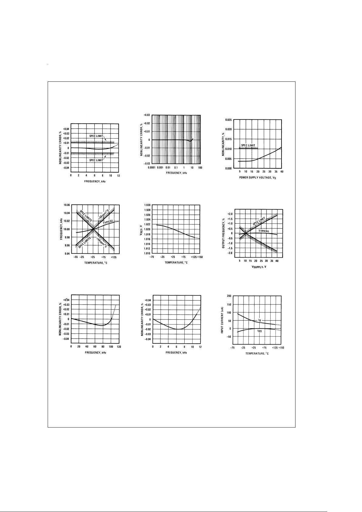
Typical Performance Characteristics
(All electrical characteristics apply for the circuit of
Figure 4
, unless otherwise noted.)
Nonlinearity Error
as Precision V-to-F
Converter (
Figure 4
)
DS005680-25
Nonlinearity Error
DS005680-26
Nonlinearity Error vs Power
Supply Voltage
DS005680-27
Frequency vs Temperature
DS005680-28
V
REF
vs Temperature
DS005680-29
Output Frequency vs
V
SUPPLY
DS005680-30
100 kHz Nonlinearity Error
(
Figure 5
)
DS005680-31
Nonlinearity Error
(
Figure 1
)
DS005680-32
Input Current (Pins 6,7) vs
Temperature
DS005680-33
www.national.com5
Page 6

Typical Performance Characteristics (Continued)
Typical Applications
PRINCIPLES OF OPERATION OF A SIMPLIFIED
VOLTAGE-TO-FREQUENCY CONVERTER
The LM231/331 are monolithic circuits designed for accuracy and versatile operation when applied as
voltage-to-frequency (V-to-F) converters or as
frequency-to-voltage (F-to-V) converters. A simplified block
diagram of the LM231/331 is shownin
Figure 3
and consists
of a switched current source, input comparator, and 1-shot
timer.
The operation of these blocks is best understood by going
through the operating cycle of the basic V-to-F converter,
Figure 3
, which consists of the simplified block diagram of
the LM231/331 and the various resistors and capacitors connected to it.
The voltage comparator compares a positive input voltage,
V1, at pin 7 to the voltage, V
x
, at pin 6. If V1 is greater, the
comparator will trigger the 1-shot timer. The output of the
timer will turn ON both the frequency output transistor and
the switched current source for a period t=1.1 R
tCt
. During
this period, the current i will flow out of the switched current
source and provide a fixed amount of charge, Q=i x t, into
the capacitor, C
L
. This will normally charge Vxup to a higher
level than V1. At the end of the timing period, the current i will
turn OFF, and the timer will reset itself.
Now there is no current flowing from pin 1, and the capacitor
C
L
will be gradually discharged by RLuntil Vxfalls to the level
of V1. Then the comparator will trigger the timer and start another cycle.
The current flowing into C
L
is exactly I
AVE
=
i x (1.1xR
tCt
)x
f, and the current flowing out ofC
L
is exactly Vx/R
L
≅
VIN/RL.
If V
IN
is doubled, the frequency will double to maintain this
balance. Even a simple V-to-F converter can provide a frequency precisely proportional to its input voltage over awide
range of frequencies.
DETAIL OF OPERATION, FUNCTIONAL BLOCK
DIAGRAM (
Figure 2
)
The block diagram shows a band gap reference which provides a stable 1.9 V
DC
output. This 1.9 VDCis well regulated
over a V
S
range of 3.9V to 40V. It also has a flat, low tem-
perature coefficient, and typically changes less than
1
⁄
2
%
over a 100˚C temperature change.
The current pump circuit forces the voltage at pin 2 to be at
1.9V, and causes a current i=1.90V/R
S
to flow. For R
s
=
14k,
i=135 µA. The precision current reflector provides a current
equal to i to the current switch. The current switch switches
the current to pin 1 or to ground depending on the state of
the R
S
flip-flop.
The timing function consists of an R
S
flip-flop, and a timer
comparator connected to the external R
tCt
network. When
the input comparator detects a voltage at pin 7 higher than
pin 6, it sets the R
S
flip-flop which turns ON the current
switch and the output driver transistor. When the voltage at
pin 5 rises to
2
⁄3VCC, the timer comparator causes the R
S
flip-flop to reset. The reset transistor is then turned ON and
the current switch is turned OFF.
However, if the input comparator still detects pin 7 higher
than pin 6 when pin 5crosses
2
⁄3VCC, the flip-flop will not be
reset, and the current at pin 1 will continue to flow, in its attempt to make the voltage at pin 6 higher than pin 7. This
Power Drain vs V
SUPPLY
DS005680-34
Output Saturation Voltage vs
I
OUT
(Pin 3)
DS005680-35
Nonlinearity Error, Precision
F-to-V Converter (
Figure 7
)
DS005680-36
DS005680-4
FIGURE 3. Simplified Block Diagram of Stand-Alone
Voltage-to-Frequency Converter and
External Components
www.national.com 6
Page 7

Typical Applications (Continued)
condition will usually apply under start-up conditions or in the
case of an overload voltage at signal input. It should be
noted that during this sort of overload, the output frequency
will be 0; as soon as the signal is restored to the working
range, the output frequency will be resumed.
The output driver transistor acts to saturate pin3 with an ON
resistance of about 50Ω. In case of overvoltage, the output
current is actively limited to less than 50 mA.
The voltage at pin 2is regulated at 1.90 V
DC
for all values of
i between 10 µA to 500 µA. It can be used as a voltage reference for other components, but care must be taken to ensure that current is not taken from it which could reduce the
accuracy of the converter.
PRINCIPLES OF OPERATION OF BASIC VOLTAGETO-FREQUENCY CONVERTER (
Figure 1
)
The simple stand-alone V-to-F converter shown in
Figure 1
includes all the basic circuitry of
Figure 3
plus a few compo-
nents for improved performance.
A resistor, R
IN
=
100 kΩ
±
10%, has been added in the path to
pin 7, so that the bias current at pin 7 (−80 nA typical) will
cancel the effect of the bias current at pin 6and help provide
minimum frequency offset.
The resistance R
S
at pin 2 is made up of a 12kΩ fixed resistorplusa5kΩ(cermet, preferably) gain adjust rheostat. The
function of this adjustment is totrim out thegain tolerance of
the LM231/331, and the tolerance of R
t,RL
and Ct.
For best results, all the components should be stable
low-temperature-coefficient components, such as metal-film
resistors. The capacitor should have low dielectric absorption; depending on the temperature characteristics desired,
NPO ceramic, polystyrene, Teflon or polypropylene are best
suited.
Acapacitor C
IN
is added from pin 7 to ground to act as a filter
for V
IN
. A value of 0.01 µFto 0.1 µFwill be adequatein most
cases; however, in cases where better filtering is required, a
1 µF capacitor can be used. When the RC time constants are
matched at pin 6 and pin 7, a voltage step at V
IN
will cause
a step change in f
OUT
.IfCINis much less than CL, a step at
V
IN
may cause f
OUT
to stop momentarily.
A47Ωresistor, in series with the 1 µF C
L
, is added to give
hysteresis effect which helps the input comparator provide
the excellent linearity (0.03%typical).
DETAIL OF OPERATION OF PRECISION V-TO-F
CONVERTER (
Figure 4
)
In this circuit, integration is performed by using a conventional operational amplifier and feedback capacitor, C
F
.
When the integrator’s output crosses the nominal threshold
level at pin 6 of the LM231/331, the timing cycle is initiated.
The average current fed into the op amp’s summing point
(pin 2) is i x (1.1 R
tCt
) x f which is perfectly balanced with
−V
IN/RIN
. In this circuit, the voltage offset of the LM231/331
input comparator does not affect the offset or accuracy of the
V-to-F converter as it does in the stand-alone V-to-F converter; nor does the LM231/331 bias current or offset current. Instead, the offset voltage and offset current of the operational amplifier are the only limits on how small the signal
can be accurately converted. Since op amps with voltage offset well below 1 mV and offset currents well below 2 nA are
available at low cost, this circuit is recommended for best accuracy for small signals. This circuit also responds immediately to any change of input signal (which a stand-alone circuit does not) so that the output frequency will be an
accurate representation of V
IN
, as quickly as 2 output pulses’
spacing can be measured.
In the precision mode, excellent linearity is obtained be-
cause the current source (pin 1) is always at ground potential
and that voltage does not vary with V
IN
or f
OUT
. (In the
stand-alone V-to-F converter, a major cause of non-linearity
is the output impedance at pin 1 which causes i to change as
a function of V
IN
).
The circuit of
Figure 5
operates in the same way as
Figure 4
,
but with the necessary changes for high speed operation.
www.national.com7
Page 8

Typical Applications (Continued)
DS005680-5
*
Use stable components with low temperature coefficients. See Typical Applications section.
**
This resistor can be 5 kΩ or 10 kΩ for V
S
=
8V to 22V, but must be 10 kΩ for V
S
=
4.5V to 8V.
***
Use low offset voltage and low offset current op amps forA1: recommended type LF411A
FIGURE 4. Standard Test Circuit and Applications Circuit, Precision Voltage-to-Frequency Converter
www.national.com 8
Page 9

Typical Applications (Continued)
DETAILS OF OPERATION, FREQUENCY-TOVOLTAGE CONVERTERS (
Figure 6
and
Figure 7
)
In these applications, a pulse input at f
IN
is differentiated by
a C-R network and the negative-going edge at pin 6 causes
the input comparator to trigger the timer circuit. Just as with
a V-to-F converter,the average current flowing out of pin1 is
I
AVERAGE
=
i x (1.1 R
tCt
)xf.
In the simple circuit of
Figure 6
, this current is filtered in the
network R
L
=
100 kΩ and 1 µF.The ripple will be less than 10
mV peak, but the response will be slow, with a 0.1 second
time constant, and settling of 0.7 second to 0.1%accuracy.
In the precision circuit, an operational amplifier provides a
buffered output and also actsas a 2-pole filter. The ripple will
be less than 5 mV peak for all frequencies above 1 kHz, and
the response time will be much quicker than in
Figure 6
.
However, for input frequencies below 200 Hz, this circuit will
have worse ripple than
Figure 6
. The engineering of the filter
time-constants to get adequate response and small enough
ripple simply requires a study of the compromises to be
made. Inherently, V-to-F converter responsecan be fast,but
F-to-V response can not.
DS005680-6
*
Use stable components with low temperature coefficients.
See Typical Applications section.
**
This resistor can be 5 kΩ or 10 kΩ for V
S
=
8V to 22V, but must be 10 kΩ for V
S
=
4.5V to 8V.
***
Use low offset voltage and low offset current op amps forA1: recommended types LF411A or LF356.
FIGURE 5. Precision Voltage-to-Frequency Converter,
100 kHz Full-Scale,
±
0.03%Non-Linearity
www.national.com9
Page 10

Typical Applications (Continued)
DS005680-7
*
Use stable components with low temperature coefficients.
FIGURE 6. Simple Frequency-to-Voltage Converter,
10 kHz Full-Scale,
±
0.06%Non-Linearity
DS005680-8
*
Use stable components with low temperature coefficients.
FIGURE 7. Precision Frequency-to-Voltage Converter,
10 kHz Full-Scale with 2-Pole Filter,
±
0.01
%
Non-Linearity Maximum
Light Intensity to Frequency Converter
DS005680-9
*
L14F-1, L14G-1 or L14H-1, photo transistor (General Electric Co.) or similar
Temperature to Frequency Converter
DS005680-10
www.national.com 10
Page 11

Typical Applications (Continued)
Long-Term Digital Integrator Using VFC
DS005680-11
Basic Analog-to-Digital Converter Using
Voltage-to-Frequency Converter
DS005680-12
Analog-to-Digital Converter with Microprocessor
DS005680-13
Remote Voltage-to-Frequency Converter with 2-Wire Transmitter and Receiver
DS005680-14
www.national.com11
Page 12

Typical Applications (Continued)
Voltage-to-Frequency Converter with Square-Wave Output Using
÷
2 Flip-Flop
DS005680-15
Voltage-to-Frequency Converter with Isolators
DS005680-16
Voltage-to-Frequency Converter with Isolators
DS005680-17
www.national.com 12
Page 13

Typical Applications (Continued)
Connection Diagram
Voltage-to-Frequency Converter with Isolators
DS005680-18
Voltage-to-Frequency Converter with Isolators
DS005680-19
Dual-In-Line Package
DS005680-21
Order Number LM231AN, LM231N, LM331AN,
or LM331N
See NS Package Number N08E
www.national.com13
Page 14

Schematic Diagram
DS005680-22
www.national.com 14
Page 15

Physical Dimensions inches (millimeters) unless otherwise noted
LIFE SUPPORT POLICY
NATIONAL’S PRODUCTS ARE NOT AUTHORIZED FOR USE AS CRITICAL COMPONENTS IN LIFE SUPPORT
DEVICES OR SYSTEMS WITHOUT THE EXPRESS WRITTEN APPROVAL OF THE PRESIDENT AND GENERAL
COUNSEL OF NATIONAL SEMICONDUCTOR CORPORATION. As used herein:
1. Life support devices or systems are devices or
systems which, (a) are intended for surgical implant
into the body, or (b) support or sustain life, and
whose failure to perform when properly used in
accordance with instructions for use provided in the
labeling, can be reasonably expected to result in a
significant injury to the user.
2. A critical component is any component of a life
support device or system whose failure to perform
can be reasonably expected to cause the failure of
the life support device or system, or to affect its
safety or effectiveness.
National Semiconductor
Corporation
Americas
Tel: 1-800-272-9959
Fax: 1-800-737-7018
Email: support@nsc.com
National Semiconductor
Europe
Fax: +49 (0) 1 80-530 85 86
Email: europe.support@nsc.com
Deutsch Tel: +49 (0) 1 80-530 85 85
English Tel: +49 (0) 1 80-532 78 32
Français Tel: +49 (0) 1 80-532 93 58
Italiano Tel: +49 (0) 1 80-534 16 80
National Semiconductor
Asia Pacific Customer
Response Group
Tel: 65-2544466
Fax: 65-2504466
Email: sea.support@nsc.com
National Semiconductor
Japan Ltd.
Tel: 81-3-5639-7560
Fax: 81-3-5639-7507
www.national.com
Dual-In-Line Package (N)
Order Number LM231AN, LM231N, LM331AN, or LM331N
NS Package N08E
LM231A/LM231/LM331A/LM331 Precision Voltage-to-Frequency Converters
National does not assume any responsibility for use of any circuitry described, no circuit patent licenses are implied and National reserves the right at any time without notice to change said circuitry and specifications.
 Loading...