

Page 1
www.DataSheet4U.net
www.DataSheet4U.net
LM230W01
Liquid Crystal Display
Product Specification
www.jxlcd.com
www.jxlcd.com
Ver. 1.0 FEB . 06 . 2003
1 / 27
Page 2
www.DataSheet4U.net
www.DataSheet4U.net
LM230W01
Liquid Crystal Display
Product Specification
Contents
PageITEMNo
COVER
CONTENTS
RECORD OF REVISIONS
GENERAL DESCRIPTION1
ABSOLUTE MAXIMUM RATINGS2
ELECTRICAL SPECIFICATIONS3
ELECTRICAL CHARACTREISTICS 3-1
INTERFACE CONNECTIONS 3-2
SIGNAL TIMING SPECIFICATIONS 3-3
SIGNAL TIMING WAVEFORMS 3-4
COLOR INPUT DATA REFERNECE 3-5
www.jxlcd.com
www.jxlcd.com
POWER SEQUENCE 3-6
OPTICAL SFECIFICATIONS4
MECHANICAL CHARACTERISTICS5
RELIABLITY6
1
2
3
4
5
6
6
8
11
12
13
14
15
19
22
Ver. 1.0 FEB . 06 . 2003
INTERNATIONAL STANDARDS7
SAFETY 7-1
EMC 7-2
PACKING8
DESIGNATION OF LOT MARK 8-1
PACKING FORM 8-2
23
23
23
24
24
24
25PRECAUTIONS9
27APPENDIX
2 / 27
Page 3
www.DataSheet4U.net
www.DataSheet4U.net
LM230W01
Liquid Crystal Display
Product Specification
RECORD OF REVISIONS
DESCRIPTIONPageRevision DateRevision No
First Draft (Preliminary)-JAN.17.20030.0
the White color coordination change ( TBD,TBD →0.314,0.331)15FEB.06.20031.0
www.jxlcd.com
www.jxlcd.com
Ver. 1.0 FEB . 06 . 2003
3 / 27
Page 4
www.DataSheet4U.net
www.DataSheet4U.net
LM230W01
Liquid Crystal Display
Product Specification
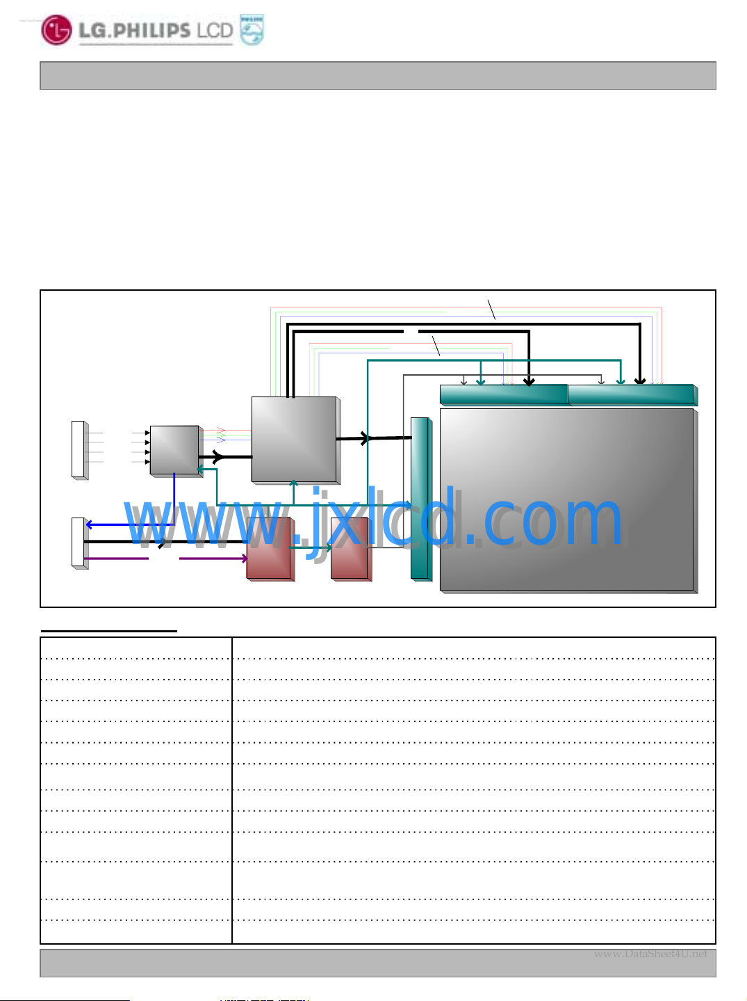
1. General Description
The LM230W01 LCD is a Color Active Matrix Liquid Crystal Display with an integral Cold Cathode Fluorescent
Lamp(CCFL) back light system. The matrix employs a-Si Thin Film Transistor as the active element. It is a tra
nsmissive type display operating in the normally black mode. This TFT-LCD has a 23.0 inch diagonally measu
red active display area with WUXGA resolution(1920 vertical by 1200 horizontal pixel array). Each pixel is divid
ed into Red, Green and Blue sub-pixels or dots which are arranged in vertical stripes. Gray scale or the lumina
nce of the sub-pixel color is determined with a 8-bit gray scale signal for each dot, thus, presenting a palette of
more than 16,777,216 colors.
The LM230W01 has been designed to apply the TMDS
erface method to enables a simple and low-cost implementation in both the host and monitor.
TM
(Transition Minimized differential Signaling) as the int
RGB (24BIT)
CLK
RGB (24B IT)
VCC, VDD
V0~ V1 7
SOURCE (Left)
SOURCE (Right)
RXC +/RX0 +/RX1 +/-
(2 0 P IN)
USER C ON
POW ER C ON
RX2 +/-
H sync, Vsyn c
(15P IN)
TM D S
TM D S
TM D STM D S
Receiver
Receiver
ReceiverR eceiver
IN P U T 1 8V
www.jxlcd.com
www.jxlcd.com
PW R _O N
General Features
RGB D ATA
CLK
Hsync
Vsyn c
Tim ing
Tim ing
Tim ingTim ing
C o n t r o lle r
C o n t r o lle r
C o n t r o lle rC o n t r o lle r
DC/DC
DC/DC
DC/DCDC/DC
C onverter
C onverter
C onverterC onverter
23.0 inches(58.4cm) diagonalActive Screen Size
550.0(H) x 360.5(V) x 25.0(D) mm(Typ.)Outline Dimension
495.36[mm] × 309.6[mm]Active Area
0.258 mm x 0.258mmPixel Pitch
1920 horiz. By 1200 vert. Pixels RGB stripes arrangementPixel Format
8-bit, 16,777,216 colorsColor Depth
200 cd/m
Total 47 Watt(Typ.)Power Consumption
4,500 g (typ.)Weight
K
L
C
PANEL
PANEL
G
A
VC C
T
VG H ,VG L
GAMMA
GAMMA
GAMMAGAMMA
2
(Typ.)Luminance, White
E
PANELPANEL
1920 X 1200
1920 X 1200
1920 X 12001920 X 1200
Surface Treatment
Ver. 1.0 FEB . 06 . 2003
Transmissive mode, normally blackDisplay Operating Mode
Hard coating(3H)
Anti-glare treatment of the front polarizer,
TMDS (Hsync/DE)Interface
6 CCFL’s(Cold Cathode Fluorescent Lamp)LAMP
4 / 27
Page 5
www.DataSheet4U.net
www.DataSheet4U.net
Liquid Crystal Display
Product Specification
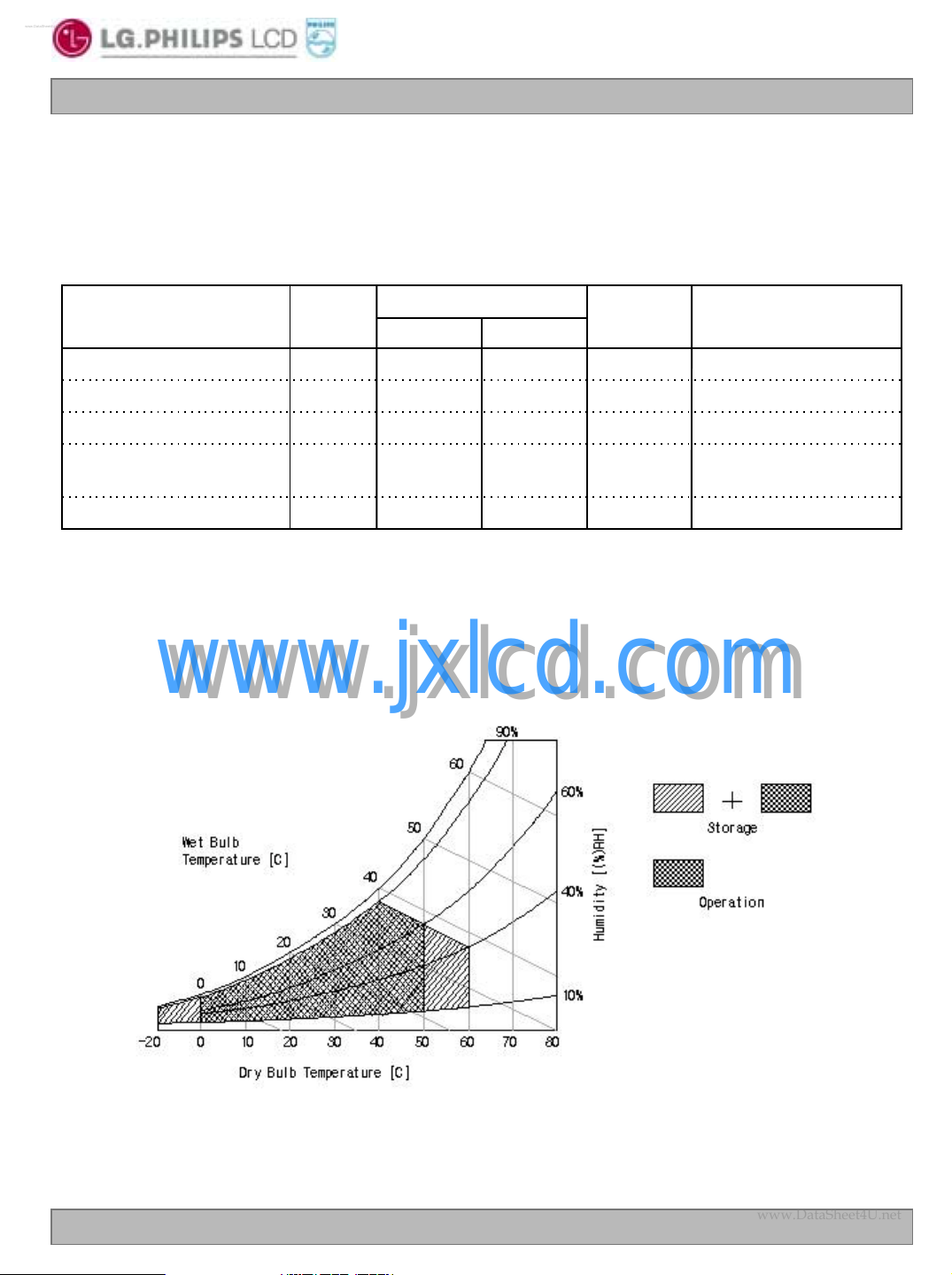
2. Absolute Maximum Ratin gs
The following are maximum values which, if exceeded, may cause operation or damage to the unit.
Table 1. ABSOLUTE MAXIMUM RATINGS
LM230W01
Parameter Notes
Power Input Voltage
Operating Temperature
Storage Temperature
Operating Ambient Humidit
y
Storage Humidity
Note : 1. Temperature and relative humidity range are shown in the figure below.
Wet bulb temperature should be 39 °C Max, and no condensation of water.
www.jxlcd.com
www.jxlcd.com
Symbol
OP
ST
OP
ST
Values
MaxMin
500T
60-20H
Units
°C
°C
at 25 ± 5°CVcc21-0.3Vcc
1
1
1%RH9010H
1%RH9010H
Ver. 1.0 FEB . 06 . 2003
5 / 27
Page 6
www.DataSheet4U.net
www.DataSheet4U.net
Liquid Crystal Display
Product Specification
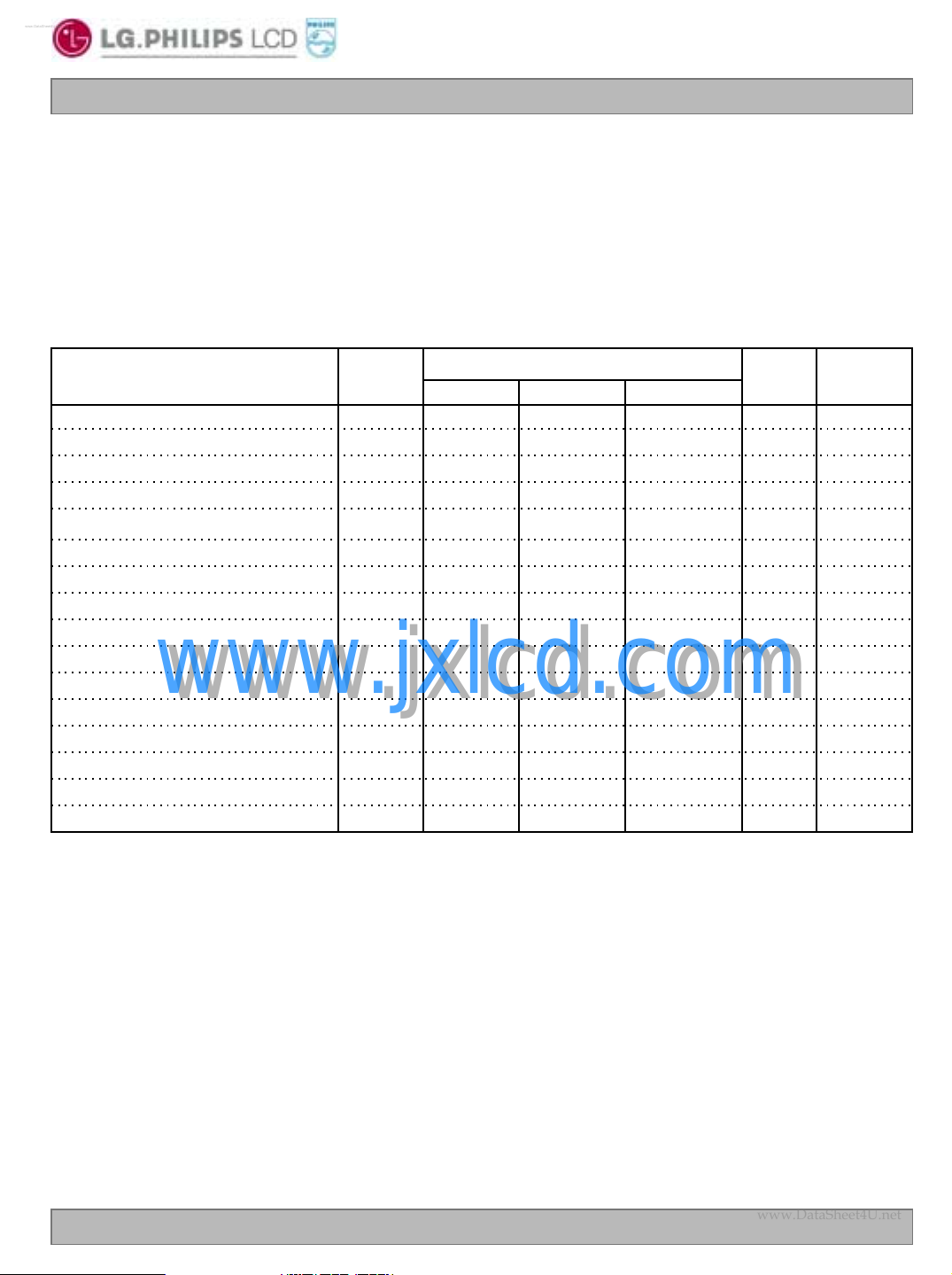
3. Electrical Specifications
3-1. Electrical Characteristics
The LM230W01 requires two power inputs. One input is employed to power the LCD electronics and to d
rive the voltages to drive the TFT array and liquid crystal. And the second input which powers the CCFL, i
s typically generated by an inverter. The inverter is an external unit to the LCD.
Table 2. ELECTRICAL CHARACTERISTICS
LM230W01
Parameter Symbol
MODULE :
Inrush Current
LAMP :
Operating Voltage
Operating Current
at 25 °C
www.jxlcd.com
www.jxlcd.com
at 0 °C
Operating Frequency
Power Consumption
Notes : 1. The input current shall be measured at V
clock frequency of 156MHz under mosaic pattern(8x6) (typ).
2. The measuring condition
The duration of rush current is about 20ms, and rising time of Power input is 1ms.
3. The variance of the voltage is ±10%.
4. Operating voltage is measured at 25°C. The variance of the voltage is ±10%.
5. The output voltage at the transformer in the inverter must be high considering to the loss of the
ballast capacitor in the inverter. The voltage above V
than 1 second for start-up. Otherwise, the lamps may not be turned on.
6. Lamp frequency may produce interface with horizontal synchronous frequency and as a result this
may cause beat on the display. Therefore lamp frequency shall be as away possible from the
horizontal synchronous frequency and from its harmonics in order to prevent interference.
7. The lamp power consumption shown above does not include loss of external inverter at 25°C.
The used lamp current is the lamp typical current.
Rush
BL
BL
BL
BL
of 18.0Vdc at 25℃, refresh rate of 60Hz, and pixel
CC
Values
MaxTypMin
Vdc19.018.017.0Vcc Power Supply Input Voltage
1090(2.5mA)875(7.5mA)830(9mA)V
1400-1960--
should be applied to the lamps for more
S
V
V
RMS
mA9.07.52.5I
RMS
RMS
NotesUnit
1A0.650.45-Icc Power Supply Input Current
1Watt11.78.1-Pc Power Consumption
2A3--I
3V
4Vs Established Starting Voltage
5kHz605040F
6Watt45.141.0-P
7min3--Ts Discharge Stabilization Time
8Hrs30,000 Life Time
Ver. 1.0 FEB . 06 . 2003
6 / 27
Page 7
www.DataSheet4U.net
www.DataSheet4U.net
Liquid Crystal Display
LM230W01
Product Specification
8. Let’s define the brightness of the lamp after being lighted for 5 minutes as 100%.
T
The used lamp current is the lamp typical current.
9. The life time is defined as the time at which brightness of lamp is 50% compare to that of initial
value at the typical lamp current on condition of continuous operating at 25±2°C.
Note. Do not attach a conducting tape to connecting wire.
If the lamp wire attach to a conducting tape, TFT-LCD Module has a low luminance and the
inverter has abnormal action. Because leakage current is occurred between lamp wire and
conducting tape.
is the time required for the brightness of the center of the lamp to be not less than 95%.
S
The design of the inverter must have specifications for the lamp in LCD Assembly.
The performance of the Lamp in LCM, for example life time or brightness, is extremely influenced by
the characteristics of the DC-AC inverter. So all the parameters of an inverter should be carefully
designed so as not to produce too much leakage current from high-voltage output of the inverter.
When you design or order the inverter, please make sure unwanted lighting caused by the mismatch
of the lamp and the inverter(no lighting, flicker, etc) never occurs. When you confirm it, the LCD –
Assembly should be operated in the same condition as installed in you instrument.
Requirements for a system inverter design, which is intended to have a better display performance, a
better power efficiency and a more reliable lamp.
It shall help increase the lamp lifetime and reduce its leakage current.
a. The asymmetry rate of the inverter current and voltage waveform should be 10% below;
b. The distortion rate of the current and voltage waveform should be within √2 ±10%;
c. The ideal sine current and voltage waveform shall be symmetric in positive and negative polarities.
* Asymmetry rate = | I
* Distortion rate = I
www.jxlcd.com
www.jxlcd.com
– I –p | / I
p
(or I –p) / I
p
rms
rms
* 100%
Ver. 1.0 FEB . 06 . 2003
7 / 27
Page 8

www.DataSheet4U.net
www.DataSheet4U.net
Liquid Crystal Display
LM230W01
Product Specification
3-2. Interface Connections
This LCD employs three kinds of interface connections. A 20 pin connector is used for TMDS signals from t
he host computer. A 15-pin connector is used for LCD module power and LCM controls signal from external
monitor control circuits. And six connectors, two pin connector, are used for the integral backlight system.
3-2-1. Sig nal Interface
The TMDS signal interface connector is FI-XL20S-HF by JAE.
The pin configuration for the 20 pin connector is shown in the table below.
Table 3 20PIN CONNECTOR (CNC6) PIN CONFIGURATION
DescriptionSymbolPinDescriptionSymbolPin
GND Shield for TMDS channel 0SHLD011Ground1
TX0+12GroundGND2
TX0-13GroundGND3
TXC+15Shield for TMDS channel 2SHLD25
TX2+6
TX2-7
TX1+9
TX1-10
TMDS positive differential output
(Channel 2)
www.jxlcd.com
www.jxlcd.com
TMDS negative differential output
(Channel 2)
TMDS positive differential output
(Channel 1)
TMDS negative differential output
(Channel 1)
TXC-16
TMDS positive differential output
(Channel 0)
TMDS negative differential output
(Channel 0)
Shield for TMDS channel CSHLDC14GroundGND4
TMDS positive differential output
(Channel C)
TMDS negative differential output
(Channel C)
GroundGND17
GroundGND18Shield for TMDS channel 1SHLD18
GroundGND19
GroundGND20
1. Interface chips
1.1 LCD : PTFP 403 PZP (TI)
2. Connector
2.1 LCD : FI-XL20S-HF
2.2 Mating : FI-XL20H or compatible
2.3 Connector pin arrangement
Notes: 1. All shield pins and GND(ground) pin should be connected together and should also be
connected to the LCD’s metal frame.
Ver. 1.0 FEB . 06 . 2003
20.1
CNC6
8 / 27
Page 9
www.DataSheet4U.net
www.DataSheet4U.net
Liquid Crystal Display
LM230W01
Product Specification
3-2-2. Power In t erf ace
A 15 pin connector (CNC7) for external monitor control circuits, is a model 53261 manufactured by Molex.
The mating connector part number is 51021 or its equivalent. The pin configuration for this connector is sho
wn in the table below.
Table 4 15 PIN CONNECTOR (CNC7) PIN CONFIGURATION
Pin
1
2
3
4
5
6
7
8
9
10
www.jxlcd.com
www.jxlcd.com
11
12
13
14
15
Symbol
GND
GND
PWR_ON
GND
Vcc
Vcc
Vcc
Vcc
GND
DDC_CLK
DDC_DAT
GND
HS_OUT
VS_OUT
GND
Description
Ground
Ground
Power ON control signal input
Ground
LCM power supply, +18V ±5%
LCM power supply, +18V ±5%
LCM power supply, +18V ±5%
LCM power supply, +18V ±5%
Ground
DDC clock line out
DDC data line out
Ground
Hsync Output
Vsync Output
Ground
5V(H:90%,L:10%)
Notes
Connector pin arrangement
Notes: 1. All GND(ground) pins should be connected together and should also be connected to the
LCD’s metal frame.
Ver. 1.0 FEB . 06 . 2003
151
CNC7
9 / 27
Page 10

www.DataSheet4U.net
www.DataSheet4U.net
Liquid Crystal Display
LM230W01
Product Specification
3-2-3. Backlig ht In t erf ace
The backlight interface connector is a model BHSR-02VS-1(CN2/CN3) and BHSR-05VS-1 (CN1/CN4) man
ufactured by JST. The mating connector part number are SM02B-BHSS-1-TB(2pin), SM04(9-E2)B-BHS-1-T
B or equivalent. The pin configuration for the connector is shown in the table below.
Table 5 BACKLIGHT CONNECTOR PIN CONFIGURATION
Symbol
CN1
5
CN2
CN3
CN4
www.jxlcd.com
www.jxlcd.com
5
Notes: 1. The high voltage power terminal is colored pink,blue,gray. Ground pin color is white.
HV
HV
NC
LV
LV
HV
LV
HV 1Power supply for lamp 4(High voltage side) - Gray1
LV
HV
HV
NC
LV
LV
NC3
Power supply for lamp 1(Low voltage side) - White4
Power supply for lamp 2(Low voltage side) - White
Power supply for lamp 3(Low voltage side) - White2
Power supply for lamp 4(Low voltage side) - White2
NC3
Power supply for lamp 5(Low voltage side) - White4
Power supply for lamp 6(Low voltage side) - White
NotesDescriptionPinNo
1Power supply for lamp 1(High voltage side) - Pink1
1Power supply for lamp 2(High voltage side) - Blue2
1Power supply for lamp 3(High voltage side) - Gray1
1Power supply for lamp 6(High voltage side) - Pink1
1Power supply for lamp 5(High voltage side) - Blue2
Ver. 1.0 FEB . 06 . 2003
Up Side
Down Side
<BACKLIGHT CONNEC TOR DIAG RAM>
Lamp1
Lamp 2
Lamp 3
Lamp 4
Lamp 5
Lamp 6
CN 1
CN 2
CN 3
CN 4
10 / 27
Page 11

www.DataSheet4U.net
www.DataSheet4U.net
LM230W01
Liquid Crystal Display
Product Specification
3-3. Signal Timing Specifications
This is signal timing required at the input of the TMDS transmitter. All of the interface signal timing should be
satisfied with the following specifications for it’s proper operation.
Table 6. Timing Table
Enable
SYMBOL
t
PeriodDCLK
Frequency
PeriodHsync
Width-Active
PeriodVsync
Frequency
Width-Active
www.jxlcd.com
www.jxlcd.com
Horizontal ValidData
Horizontal Back Porch
Horizontal Front Porch
Horizontal Blank
CLK
CLK
f
t
t
t
t
t
t
HBP
HFP
t
HP
WH
VP
V
f
WV
HV
-
6.336.416.49
158156154
-21441984
323232
-12121206
646056
-32
192019201920
-12816
-6416
-22464
Ns
MHz
t
CLK
t
HP
Hz
t
HP
CLK
t
NoteUnitMaxTypMinITEM
1
2
3
4
t
WH+ tHBP+ tHFP
Notes: 1. Hsync period shall be a double number of 8
2. Horizontal sync shall be active high.
3. Vertical frequency should be keep the above specification when the resolution & mode are changed.
4. Vertical sync shall be active high.
Ver. 1.0 FEB . 06 . 2003
Vertical Valid
Vertical Back Porch
Vertical Front Porch
Vertical Blank
t
t
t
VV
VBP
VFP
-
120012001200
-63
t
HP
-31
WV+ tVBP+ tVFP
-126
t
11 / 27
Page 12

www.DataSheet4U.net
www.DataSheet4U.net
3-4. Signal Timing Waveforms
LM230W01
Liquid Crystal Display
Product Specification
Hsync, Vsync, DE, DATA
t
CLK
Dclk
INVALID
DATA
DE(Data Enable)
www.jxlcd.com
www.jxlcd.com
Hsync
t
WH
0.5V
CC
0.7Vcc
0.3Vcc
VALID
Data are latched at the fall i ng edge of DCLK
t
HP
INVALID
DE(Data Enable)
Vsync
DE(Data Enable)
Ver. 1.0 FEB . 06 . 2003
t
WV
t
VBP
t
HBP
t
HV
t
VP
t
VV
t
HFP
t
VFP
12 / 27
Page 13

www.DataSheet4U.net
www.DataSheet4U.net
Liquid Crystal Display
LM230W01
Product Specification
3-5. Color Input Data Reference
The brightness of each primary color(red,green and blue) is based on the 8-bit gray scale data input for the
color ; the higher the binary input, the brighter the color. The table below provides a reference for color
versus data input.
Table 7. COLOR DATA REFERENCE
Input Color Data
Basic
Color
RED
GREEN
BLUE
Color
Black
Red (255)
Green (255)
Blue (255)
Cyan
Magenta
Yellow
White
www.jxlcd.com
www.jxlcd.com
RED (000)
RED (001)
...
RED (254)
RED (255)
GREEN (000)
GREEN (001)
...
GREEN (254)
GREEN (255)
BLUE (000)
BLUE (001)
...
BLUE (254)
BLUE (255)
MSB LSB
RED
MSB LSB
GREEN
MSB LSB
B7 B6 B5 B4 B3 B2 B1 B0G7 G6 G5 G4 G3 G2 G1 G0R7 R6 R5 R4 R3 R2 R1 R0
0 0 0 0 0 0 0 00 0 0 0 0 0 0 00 0 0 0 0 0 0 0
0 0 0 0 0 0 0 00 0 0 0 0 0 0 01 1 1 1 1 1 1 1
0 0 0 0 0 0 0 01 1 1 1 1 1 1 10 0 0 0 0 0 0 0
1 1 1 1 1 1 1 10 0 0 0 0 0 0 00 0 0 0 0 0 0 0
1 1 1 1 1 1 1 11 1 1 1 1 1 1 10 0 0 0 0 0 0 0
1 1 1 1 1 1 1 10 0 0 0 0 0 0 01 1 1 1 1 1 1 1
0 0 0 0 0 0 0 01 1 1 1 1 1 1 11 1 1 1 1 1 1 1
1 1 1 1 1 1 1 11 1 1 1 1 1 1 11 1 1 1 1 1 1 1
0 0 0 0 0 0 0 00 0 0 0 0 0 0 00 0 0 0 0 0 0 0
0 0 0 0 0 0 0 00 0 0 0 0 0 0 00 0 0 0 0 0 0 1
0 0 0 0 0 0 0 00 0 0 0 0 0 0 01 1 1 1 1 1 1 0
0 0 0 0 0 0 0 00 0 0 0 0 0 0 01 1 1 1 1 1 1 1
0 0 0 0 0 0 0 00 0 0 0 0 0 0 00 0 0 0 0 0 0 0
0 0 0 0 0 0 0 00 0 0 0 0 0 0 10 0 0 0 0 0 0 0
0 0 0 0 0 0 0 01 1 1 1 1 1 1 00 0 0 0 0 0 0 0
0 0 0 0 0 0 0 01 1 1 1 1 1 1 10 0 0 0 0 0 0 0
0 0 0 0 0 0 0 00 0 0 0 0 0 0 00 0 0 0 0 0 0 0
0 0 0 0 0 0 0 10 0 0 0 0 0 0 00 0 0 0 0 0 0 0
1 1 1 1 1 1 1 00 0 0 0 0 0 0 00 0 0 0 0 0 0 0
1 1 1 1 1 1 1 10 0 0 0 0 0 0 00 0 0 0 0 0 0 0
BLUE
.........
.........
.........
Ver. 1.0 FEB . 06 . 2003
13 / 27
Page 14

www.DataSheet4U.net
www.DataSheet4U.net
3-6. Power Sequence
LM230W01
Liquid Crystal Display
Product Specification
V
CC
90%
90%
Power Supply, V
Interface Signal, V
(Digital RGB signal,
SCDT ,V
Clock to PanelLink
Transmitter)
PWR_CTRL signal
for LCM power down
Power Supply for Backlight
Inverter
sync
CC
i
, H
, DE,
sync
www.jxlcd.com
www.jxlcd.com
Parameter
T7
T8
T9
0V
0V
10%
T1
T2
10%
T4
LAMP OFF LAMP OFF
400
50
-
Customers can monitor H
T3
5V
90%
LAMP ON
( Monitoring
T6
T5
Values
-
-
-
sync
Invalid Period
H
sync
)
,V
sync
T7
, ,V
T3
sync
,
T4
with VCC on.
Valid PeriodValid Period
MaxTypMin
--100T4
-
-
10
10%
T9
T8
T6
T5
Units
ms10--T1
ms--50T2
ms50--T3
ms
ms50--T5
ms80--T6
ms
Notes : 1. Please avoid floating state of interface signal at invalid period.
2. When the interface signal is invalid, be sure to pull down the power
supply for LCD V
3. Lamp power must be turn on after power supply for LCD and
interface signal are valid.
4. When connector is hot-plug and plug,T2 & T8 min spec can be 0ms.
Ver. 1.0 FEB . 06 . 2003
to 0V.
CC
14 / 27
Page 15

www.DataSheet4U.net
www.DataSheet4U.net
Liquid Crystal Display
LM230W01
Product Specification
4. Optical Specifications
Optical characteristics are determined after the unit has been ‘ON’ and stable for approximately 30 minutes
in a dark environment at 25 °C. The values specified are at an approximate distance 50cm from the LCD
surface at a viewing angle of Φ and θ equal to 0 ° and aperture 1 degree.
FIG. 1 presents additional information concerning the measurement equipment and method.
FIG. 1 Optical Characteristic Measurement Equipment and Method
Optical Stage(x,y)
LCD Module
Parameter Symbol NotesUnits
www.jxlcd.com
Surface Luminance, white
Luminance Variation
Color Coordinates
Viewing Angle
www.jxlcd.com
Rise Time
Decay Time
x axis, right(φ=0°) 5degree85θr
x axis, left (φ=180°)
y axis, up (φ=90°)
y axis, down (φ=270°)
500mm
RED
GREEN
BLUE
Field = 1 °
Table 8. OPTICAL CHARACTERISTICS
WH
WHITE
R
D
°
°°
Prichard 880 or
equivalent
Values
200170L
85θl
85θu
85θd
(Ta=25 °C, VCC=18.0V, fV=60Hz
Dclk=156MHz, IBL=7.5mA)
MAxTypMin
1400300CRContrast Ratio
2
(23)13Tr
(22)12Tr
0.6670.6370.607RX
0.3600.3300.300RY
0.3330.3030.273GX
0.6160.5860.556GY
0.1750.1450.115BX
0.1000.0700.040BY
0.3440.3140.284WXWHITE
0.3610.3310.301WY
2cd/m
335%δ
4ms4525TrResponse Time
62.2Gray Scale
Ver. 1.0 FEB . 06 . 2003
15 / 27
Page 16

www.DataSheet4U.net
www.DataSheet4U.net
LM230W01
Liquid Crystal Display
Product Specification
Notes :
1. Contrast Ratio(CR) is defined mathematically as :
Surface Luminance with all white pixels
Contrast Ratio =
Surface Luminance with all black pixels
Contrast ratio shall be measured at the center of the display (Location P1).
2. Average Luminance (L
displaying white
LWH=
3. The variation in surface luminance, δWHITE is defined as
Maximum (P1, P2, ....P13) - Minimum (P1, P2, ....P13)
δWHITE = X 100
Average(P1, P2, ....P5)
Where P1 to P13 are the luminance with all pixels displaying white at 13 locations.
www.jxlcd.com
www.jxlcd.com
H/16H/16
)is average of luminance value at location P1 to P5 with all pixels
WH
P1 + P2 + P3 + P4 + P5
5
H/2 H/4
P6 P7
P2
P9 P1 P10
P4 P5
P11 P12P13
Ver. 1.0 FEB . 06 . 2003
P3
P8
V/10
V/2
V/4
V/10
16 / 27
Page 17

www.DataSheet4U.net
www.DataSheet4U.net
LM230W01
Liquid Crystal Display
Product Specification
4. The response time is defined as the following figure and shall be measured by switching
the input signal for “black” and “white”.
100
90
Optical
Response
10
0
white
5. Viewing angle is the angle at which the contrast ratio is greater than 10.
φ
(12:00)
www.jxlcd.com
www.jxlcd.com
TrD TrR
black
= 0。
θ
= 90。
yu
z
A
θ
φ
white
Ver. 1.0 FEB . 06 . 2003
φ
= 180。
xl
(9:00)
TFT LCD
MODULE
z' yd
= 270。
φ
(6:00)
φ
= 0。
(3:00)
xr
17 / 27
Page 18

www.DataSheet4U.net
www.DataSheet4U.net
LM230W01
Liquid Crystal Display
Product Specification
6. Grayscale Specification
Relative Luminance [%] (Typ.)Gray Level
0.30
31
63
95
127
159
191
223
www.jxlcd.com
255
www.jxlcd.com
1.2
4.7
11.7
21.2
35.2
53.0
75.4
100
Ver. 1.0 FEB . 06 . 2003
18 / 27
Page 19

www.DataSheet4U.net
www.DataSheet4U.net
Product Specification
5. Mechanic al Characteristics
The contents provide general mechanical characteristics for the model LM230W01. In addition
the figures in the next page are detailed mechanical drawing of the LCD.
550.0 +0.7/-0.5mmHorizontal
LM230W01
Liquid Crystal Display
Outline Dimension
Bezel Area
Active Display Area
Surface Treatment
www.jxlcd.com
www.jxlcd.com
Hard coating(3H)
Anti-glare treatment of the front polarizer
360.5 +0.7/-0.5mmVertical
25.0 ± 0.7mmDepth
499.4mmHorizontal
313.6mmVertical
495.36mmHorizontal
309.6mmVertical
5000g (Max.)4500g (Typ.)Weight
Ver. 1.0 FEB . 06 . 2003
19 / 27
Page 20

www.DataSheet4U.net
www.DataSheet4U.net
<FRONT VIEW>
LM230W01
Liquid Crystal Display
Product Specification
www.jxlcd.com
www.jxlcd.com
Ver. 1.0 FEB . 06 . 2003
20 / 27
Page 21

www.DataSheet4U.net
www.DataSheet4U.net
LM230W01
Liquid Crystal Display
Product Specification
<REAR VIEW>
www.jxlcd.com
www.jxlcd.com
Ver. 1.0 FEB . 06 . 2003
21 / 27
Page 22

www.DataSheet4U.net
www.DataSheet4U.net
6. Reliability
Environment test condition
No Test Item Condition
LM230W01
Liquid Crystal Display
Product Specification
1
2
3
4
5
6
{ Result Evaluation Criteria }
There should be no change which might affect the practical display function when the display quality
test is conducted under normal operating condition.
Vibration test
(non-operating)
Shock test
(non-operating)
Altitude
storage / shipment
www.jxlcd.com
www.jxlcd.com
Ta= 60°C 240hHigh temperature storage test
Ta= -20°C 240hLow temperature storage test
Ta= 50°C 50%RH 240hHigh temperature operation test
Ta= 0°C 240hLow temperature operation test
Wave form : random
Vibration level : 1.0G RMS
Bandwidth : 10-500Hz
Duration : X,Y,Z, 10 min
One time each direction
Shock level : 100G
Waveform : half sine wave, 2ms
Direction : ±X, ±Y, ±Z
One time each direction
0 - 40,000 feet(12,192m)
Ver. 1.0 FEB . 06 . 2003
22 / 27
Page 23

www.DataSheet4U.net
www.DataSheet4U.net
Liquid Crystal Display
Product Specification
7. Intern ational Standards
7-1. Safety
a) UL 1950 Third Edition, Underwriters Laboratories, Inc. Jan. 28, 1995.
Standard for Safety of Information Technology Equipment Including Electrical Business Equipment.
b) CAN/CSA C22.2 No. 950-95 Third Edition, Canadian Standards Association, Jan. 28, 1995.
Standard for Safety of Information Technology Equipment Including Electrical Business Equipment.
c) EN 60950 : 1992+A1: 1993+A2: 1993+A3: 1995+A4: 1997+A11: 1997
IEC 950 : 1991+A1: 1992+A2: 1993+A3: 1995+A4: 1996
European Committee for Electrotechnical Standardization(CENELEC)
EUROPEAN STANDARD for Safety of Information Technology Equipment Including Electrical
Business Equipment.
7-2. EMC
a) ANSI C63.4 “Methods of Measurement of Radio-Noise Emissions from Low-Voltage Electrical
and Electrical Equipment in the Range of 9kHZ to 40GHz. “American National Standards
Institute(ANSI), 1992
b) C.I.S.P.R “Limits and Methods of Measurement of Radio Interface Characteristics of
Information Technology Equipment.“ International Special Committee on Radio Interference
c) EN 55022 “Limits and Methods of Measurement of Radio Interface Characteristics of
Information Technology Equipment.“ European Committee for Electrotechnical Standardization
(CENELEC), 1998
www.jxlcd.com
www.jxlcd.com
LM230W01
Ver. 1.0 FEB . 06 . 2003
23 / 27
Page 24

www.DataSheet4U.net
www.DataSheet4U.net
8. Packing
8-1. Designation of Lot Mark
a) Lot Mark
ABCDEFGHI JKLM
A,B,C : SIZE
D : YEAR
E : MONTH
F,G : PANEL CODE
H : ASSEMBLY CODE
I,J,K,L,M : SERIAL NO.
Note:
1. YEAR
LM230W01
Liquid Crystal Display
Product Specification
YEAR
Mark
www.jxlcd.com
2. MONTH
MONTH
Mark
3. Serial No.
Serial No.
Mark
b) Location of Lot Mark
Serial NO. is printed on the label. The label is attached to the backside of the LCD module.
This is subject to change without prior notice.
8-2. Packing Form
a) Package quantity in one box : 3 pcs
977988999200002001120022200332004420055200662007
www.jxlcd.com
Jan.1Feb.2Mar.3Apr.4May.5Jun.6Jul.7Aug.8Sep.9Oct.ANov.BDec.
1 ~ 99999
00001 ~ 99999
100000 ~
A0001 ~ A9999,·········, Z9999
7
C
b) Box Size : TBD
Ver. 1.0 FEB . 06 . 2003
24 / 27
Page 25

www.DataSheet4U.net
www.DataSheet4U.net
Liquid Crystal Display
Product Specification
9. PRECAUTIONS
Please pay attention to the following when you use this TFT LCD module.
9-1. MOUNTING PRECAUTIONS
(1) You must mount a module using holes arranged in four corners or four sides.
(2) You should consider the mounting structure so that uneven force(ex. Twisted stress) is not applied
to the module.
And the case on which a module is mounted should have sufficient strength so that external force
is not transmitted directly to the module.
(3) Please attach a transparent protective plate to the surface in order to protect the polarizer.
Transparent protective plate should have sufficient strength in order to the resist external force.
(4) You should adopt radiation structure to satisfy the temperature specification.
(5) Acetic acid type and chlorine type materials for the cover case are not describe because the former
generates corrosive gas of attacking the polarizer at high temperature and the latter causes circuit
break by electro-chemical reaction.
(6) Do not touch, push or rub the exposed polarizers with glass, tweezers or anything harder than HB
pencil lead. And please do not rub with dust clothes with chemical treatment.
Do not touch the surface of polarizer for bare hand or greasy cloth.(Some cosmetics are determined
to the polarizer.)
(7) When the surface becomes dusty, please wipe gently with absorbent cotton or other soft materials
like chamois soaks with petroleum benzene. Only IPS is recommended for cleaning the
adhesives used to attach front / rear polarizers. Do not use acetone, toluene and alcohol because
they cause chemical damage to the polarizer.
(8) Wipe off saliva or water drops as soon as possible. Their long time contact with polarizer causes
deformations and color fading.
(9) Do not open the case because inside circuits do not have sufficient strength.
www.jxlcd.com
www.jxlcd.com
LM230W01
9-2. OPERATING PRECAUTIONS
(1) The spike noise causes the mis-operation of circuits. It should be lower than following voltage :
V=±200mV(Over and under shoot voltage)
(2) Response time depends on the temperature.(In lower temperature, it becomes longer.)
(3) Brightness depends on the temperature. (In lower temperature, it becomes lower.)
And in lower temperature, response time(required time that brightness is stable after turned on)
becomes longer.
(4) Be careful for condensation at sudden temperature change. Condensation makes damage to
polarizer or electrical contacted parts. And after fading condensation, smear or spot will occur.
(5) When fixed patterns are displayed for a long time, remnant image is likely to occur.
(6) Module has high frequency circuits. Sufficient suppression to the electromagnetic interference
shall be done by system manufacturers. Grounding and shielding methods may be important to
minimized the interference.
Ver. 1.0 FEB . 06 . 2003
25 / 27
Page 26

www.DataSheet4U.net
www.DataSheet4U.net
Liquid Crystal Display
Product Specification
9-3. ELECTROSTATIC DISCHARGE CONTROL
Since a module is composed of electronic circuits, it is not strong to electrostatic discharge. Make certain
that treatment persons are connected to ground through wrist band etc. And don’t touch interface pin directly.
9-4. PRECAUTIONS FOR STRONG LIGHT E XPOSURE
Strong light exposure causes degradation of polarizer and color filter.
9-5. STORAGE
When storing modules as spares for a long time, the following precautions are necessary.
(1) Store them in a dark place. Do not expose the module to sunlight or fluorescent light. Keep the
temperature between 5°C and 35°C at normal humidity.
(2) The polarizer surface should not come in contact with any other object.
It is recommended that they be stored in the container in which they were shipped.
LM230W01
9-6. HANDLING PRECAUTIONS FOR PROTECTION FILM
(1) The protection film is attached to the bezel with a small masking tape
When the protection film is peeled off, static electricity is generated between the film and polarizer.
This should be peeled off slowly and carefully by people who are electrically grounded and with well
ion-blown equipment or in such a condition, etc.
(2) When the module with protection film attached is stored for a long time, sometimes there remains a
very small amount of glue still on the bezel after the protection film is peeled off.
(3) You can remove the glue easily. When the glue remains on the bezel or its vestige is recognized,
please wipe them off with absorbent cotton waste or other soft material like chamois
soaked with normal-hexane.
www.jxlcd.com
www.jxlcd.com
Ver. 1.0 FEB . 06 . 2003
26 / 27
Page 27

www.DataSheet4U.net
www.DataSheet4U.net
Product Specification
APPENDIX 1 : Required Signal Assi gnment for TMDS
LM230W01
Liquid Crystal Display
www.jxlcd.com
www.jxlcd.com
Ver. 1.0 FEB . 06 . 2003
27 / 27
 Loading...