

Page 1
LM124
LOW POWER QUAD OPERATIONAL AMPLIFIERS
.WIDEGAINBANDWIDTH : 1.3MHz
.INPUTCOMMON-MODE VOLTAGERANGE
INCLUDES GROUND
.LARGEVOLTAGE GAIN : 100dB
.VERYLOWSUPPLYCURRENT/AMPLI: 375µA
.LOW INPUT BIAS CURRENT : 20nA
.LOW INPUT OFFSETVOLTAGE: 5mV max.
(for more accurate applications,use theequivalent parts
LM124A-LM224A-LM324A which feature3mV max)
.LOW INPUT OFFSETCURRENT : 2nA
.WIDEPOWERSUPPLYRANGE:
SINGLESUPPLY: +3V TO +30V
DUALSUPPLIES: ±1.5VTO ±15V
LM224 - LM324
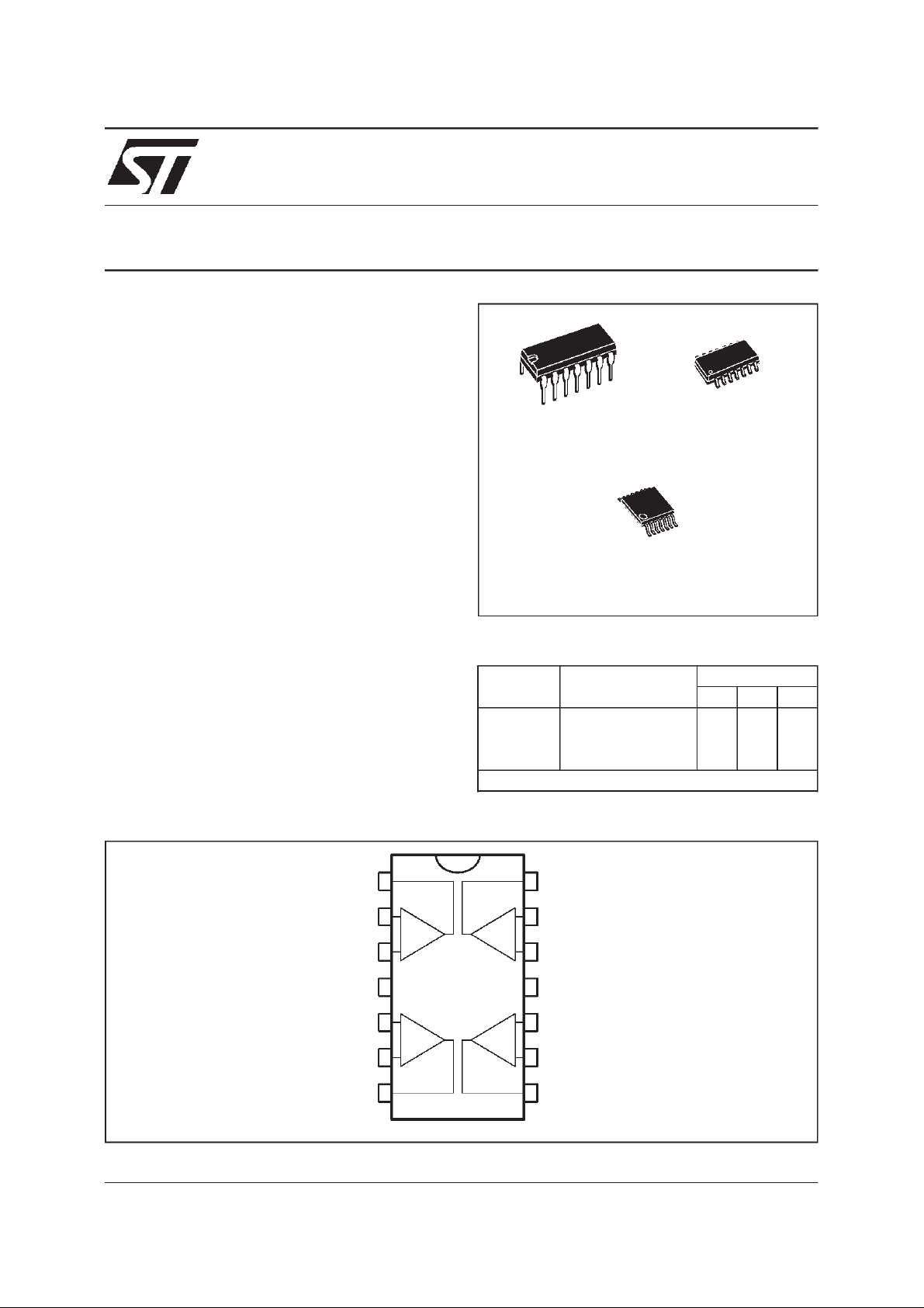
N
DIP14
(PlasticPackage)
(Thin Shrink Small Outline Package)
(PlasticMicropackage)
P
TSSOP14
D
SO14
DESC RIP TI ON
These circuits consist of four independent, high
gain,internally frequencycompensatedoperational
amplifiers.Theyoperatefromasinglepowersupply
over awide rangeof voltages.Operationfromsplit
powersupplies is also possible and the low power
supply current drain is independentof the magnitude of the power supplyvoltage.
PI N CONNECT I O NS ( top view)
Output 1
Inverting Input 1
Non-inverting Input 1
V
Non-inverting Input 2
Inverting Input 2
Output 2
CC
1
2
3
+
4
5
6
7
-
+
+
-
ORDER CODES
Part
Number
LM124 -55
LM224 -40
LM324 0
Example : LM224N
Output 4
14
Inverting Input 4
13
-
+
+
-
Non-inverting Input 4
12
V
11
Non-inverting Input 3
10
Inverting Input 3
9
Output 3
8
Temperature
Range
o
C, +125oC •••
o
C, +105oC •••
o
C, +70oC •••
-
CC
Package
NDP
June 1999
1/14
Page 2
LM124 - LM224 - LM324
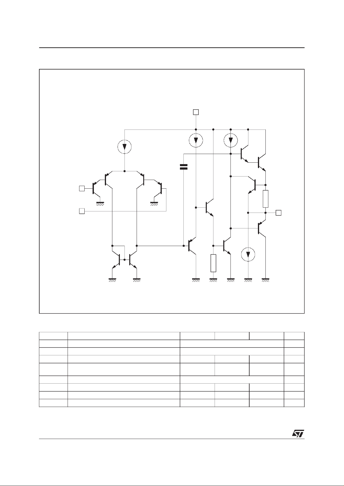
SCHE MATIC DI AG RAM (1/4 L M124)
V
CC
Inverting
input
Non-inverting
input
6µA
Q2
Q3
Q8 Q9
4µA
100µA
Q5
C
C
Q4Q1
Q7
Q6
R
SC
Q11
Output
Q13
Q10
Q12
50µA
GND
ABSOLUTE MAXIMUM RATINGS
Symbol Parameter LM124 LM224 LM324 Unit
V
V
V
P
- Output Short-circuit Duration - (note 1) Infinite
I
in
T
oper
T
stg
2/14
Supply Voltage ±16 or 32 V
cc
Input Voltage -0.3 to +32 V
i
Differential Input Voltage - (*) +32 +32 +32 V
id
Power Dissipation N Suffix
tot
D Suffix
500
-
500
400
Input Current – (note 6) 50 50 50 mA
Operating Free Air Temperature Range -55 to +125 -40 to +105 0 to +70
Storage Temperature Range -65 to +150 -65 to +150 -65 to +150
500
400
mW
mW
o
C
o
C
Page 3
ELECTRICAL CHARACTERISTICS
V
CC
+
= +5V, V
–
= Ground, VO= 1.4V, T
CC
= +25oC (unless otherwise specified)
amb
LM124 - LM224 - LM324
Symbol Parameter
V
io
I
io
I
ib
A
vd
SVR Supply Voltage Rejection Ratio (R
I
CC
V
icm
Input Offset Voltage (note 3)
=+25oC
T
T
amb
min.
≤ T
amb
≤ T
max
.
LM324
LM324
Input Offset Current
=+25oC
T
amb
≤ T
≤ T
T
min.
amb
max
.
Input Bias Current (note 2)
=+25oC
T
amb
≤ T
≤ T
≤ T
≤ T
max
max
max
.
.
.
T
min.
amb
Large Signal Voltage Gain
+
= +15V, RL=2kΩ,VO= 1.4V to 11.4V)
(V
CC
=+25oC
T
amb
≤ T
T
min.
amb
+
= 5V to 30V)
(V
CC
=+25oC
T
amb
≤ T
T
min.
amb
Supply Current, all Amp, no load
=+25oCV
T
T
amb
min.
≤ T
amb
≤ T
.VCC= +5V
max
CC
V
CC
V
CC
Input Common Mode Voltage Range
= +30V) - (note 4)
(V
CC
=+25oC
T
amb
≤ T
T
min.
amb
≤ T
max.
CMR Common-mode Rejection Ratio (R
=+25oC
T
amb
≤ T
≤ T
amb
max
= +15V, Vo= +2V 20 40 70
= +15V, Vo=+2V
= +15V, Vo= +0.2V
I
source
I
sink
T
min.
Output Current Source (Vid= +1V)
V
CC
Output Sink Current (Vid= -1V)
V
CC
V
CC
≤ 10kΩ)
S
= +5V
= +30V
= +30V
≤ 10kΩ)
S
LM124 - LM224 - LM324
Min. Typ. Max.
25
7
7
9
230
100
20 150
300
50
100
25
65
110
65
70
0.7
1.5
0.8
1.5
0
0
80
1.2
3
1.2
3
VCC-1.5
V
CC
60
10
12
20
50
Unit
mV
nA
nA
V/mV
dB
mA
V
-2
dB
mA
mA
µA
3/14
Page 4
LM124 - LM224 - LM324
ELECTRICAL CHARACTERISTICS (continued)
Symbol Parameter
V
OH
V
OL
High Level Output Voltage
= +30V)
(V
CC
= +25oCR
T
amb
. ≤ T
T
min
= +25oCR
T
amb
. ≤ T
T
min
= +5V, RL=2kΩ)
(V
CC
= +25oC
T
amb
. ≤ T
T
min
amb
amb
amb
≤ T
≤ T
≤ T
max
max
max
.
.
.
=2kΩ
L
= 10kΩ
L
Low Level Output Voltage (RL= 10kΩ)
= +25oC
T
amb
. ≤ T
T
min
amb
≤ T
max
.
SR Slew Rate
= 15V, VI= 0.5 to 3V, RL=2kΩ,CL= 100pF,
V
CC
unity gain) 0.4
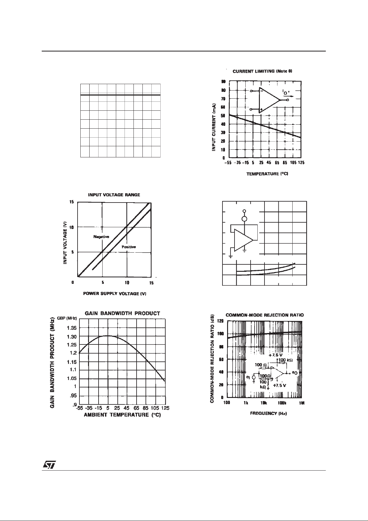
GBP Gain Bandwidth Product
= 30V, f = 100kHz, Vin= 10mV
V
CC
=2kΩ,CL= 100pF 1.3
R
L
THD Total Harmonic Distortion
f = 1kHz, A
CL= 100pF, VCC= 30V 0.015
e
n
DV
DI
IO
1/VO2 Channel Separation (note 5)
V
O
Notes : 1. Short-circuits from the output to VCCcan cause excessive heati ng if VCC> 15V. The maximum output current
Equivalent Input Noise Voltage
f = 1kHz, R
Input Offset Voltage Drift 7 30 µV/oC
io
Input Offset Current Drift 10 200 pA/oC
1kHz ≤ f ≤ 20kHz 120
is approximately 40mA i ndependent of the m agnitude of V
neous short-circuit on all amplifiers.
2. The dir ection of the input current is out of the IC . This current is essentially constant, independent of the state
of the output so no loading change exists on the i nput l ines.
= 1.4V, Rs=0Ω, 5V < V
3. V
o
4. The input common-mode voltage of either input signal voltage should not be allowed to go negative by more
than 0.3V. The upper end of the common-mode voltage range i s V
to + 32V wi thout damage.
5. Due t o the proximity of external components insure that coupling i s not originating via stray capacitance between these ext ernal parts. This typically can be detected as this t ype of capacitance increases at higher frequen ces.
6. This input current only exists when the voltage at any of t he i nput leads is driven negative. It is due to the
collector-base junction of the input PN P transistor becoming forward biased and thereby acting as input diodes clamps. I n addition to this diode action, there is also NPN parasitic act ion on the IC chip. t his t ransistor
act ion c a n cause t he ou t put voltag es of the Op- amps to go to the V
overdrive) for the time duration than an input i s dr iven negative.
This i s not destructive and normal output wi ll set up again f or input voltage higher than -0.3V.
= 20dB, RL=2kΩ,VO=2V
V
= 100Ω,VCC= 30V 40
s
+
<30V,0<Vic<V
CC
pp
CC
+
-1.5V
CC
LM124 - LM224 - LM324
Min. Typ. Max.
Unit
V
26
27
26
27
28
27
3.5
3
mV
520
20
V/µs
MHz
%
nV
√Hz
dB
. Des tr ucti v e diss ipation can r esult from sim ulta-
+
- 1.5V, but either or both inputs can go
CC
voltage l evel (or to ground for a large
CC
4/14
Page 5
IB (nA)
INPUT BIAS CURRENT
versus AMBIENT TEMPERATURE
24
21
18
15
12
9
6
3
0
-55-35-15 5 25 45 65 85 105 125
AMBIENT TEMPERATURE
(
C)
LM124 - LM224 - LM324
SUPPLY CURRENT
4
V
CC
I
D
mA
3
-
2
1
SUPPLY CURRENT (mA)
+
T
=0 Cto+125 C
amb
T
=-55 C
amb
0102030
POSITIVE SUPPLY VOLTAGE (V)
5/14
Page 6

LM124 - LM224 - LM324
6/14
Page 7

LM124 - LM224 - LM324
TYP ICAL S ING L E - S UP PLY APPLIC ATI O NS
AC COUPLED INVERTING AMPLIFIER
R
f
Ω
100k
R1
C
I
10kΩ
1/4
LM124
R
B
e
~
I
R2
Ω
100k
V
CC
C1
10
µF
100k
6.2kΩ
R3
Ω
R
f
A=-
V
R1
(asshown A = -10)
V
C
o
0
e
o
R
L
Ω
10k
2V
PP
AC COUPLED NON-INVERTING AMPLIFIER
C1
0.1µF
R1
100k
C
I
e
~
I
1M
C2
10µF
R3
R2
1M
Ω
Ω
1/4
LM124
R
B
6.2k
Ω
Ω
R4
100k
Ω
V
CC
R5
100k
Ω
R2
A=1+
V
R1
(as s hown A = 11)
V
C
o
0
e
o
R
L
10k
Ω
2V
PP
7/14
Page 8

LM124 - LM224 - LM324
TYP ICAL S ING L E - S UP PLY APPLIC ATI O NS
NON-INVERTING DC GAIN
R2
A
=1+
V
10k
Ω
e
O
1/4
LM124
+5V
R1
(As shown = 101)
A
V
DC SUMMING AMPLIFIER
100kΩ
e
1
100kΩ
100kΩ
e
2
1/4
LM124
e
O
R1
10kΩ
R2
1MΩ
(V)
e
O
0
e
(mV)
I
HIGH INPUT Z ADJUSTABLE GAIN DC
INSTRUMENTATION AMPLIFIER
R1
100k
Ω
R3
100k
1/4
e
1
R2
2k
Ω
if R1=R5and R3=R4=R6=R
eo=[1+
e
2
As shown e
LM124
Gain adjust
100k
1/4
2R
1
LM124
] (e2− e1)
R
2
= 101 (e2-e1).
o
R5
Ω
R6
100k
Ω
7
Ω
1/4
LM124
R7
100k
100k
Ω
R4
100kΩ
e
3
100kΩ
Ω
100k
e
4
eo=e1+e2-e3-e
where (e1+e2)≥ (e3+e4)
to keep e
≥ 0V
o
4
LOW DRIFT PEAK DETECTOR
I
B
1/4
I
LM124
Ω
e
O
* Polycarbonate or polyethylene
1/4
LM124
e
I
Z
I
1
F
µ
2I
R
Ω
1M
B
0.001µF
I
B
3R
3MΩ
I
B
Z
LM124
C
2I
B
*
2N 929
B
o
1/4
Inputcurrent
compensation
e
o
8/14
Page 9

LM124 - LM224 - LM324
USING SYMMETRICAL AMPLIFIERS TO REDUCE INPUT CURRENT (GENERALCONCEPT)
e
I
1.5M
1/4
e
I
2N 929
I
B
LM124
I
I
B
o
0.001µF
I
B
I
B
3MΩ
1/4
LM124
Aux. amplifier for input
I
B
current compensation
Ω
9/14
Page 10

LM124 - LM224 - LM324
TYP ICAL S ING L E - S UP PLY APPLIC ATI O NS
ACTIVER BANDPASS FILTER
R1
Ω
100k
C1
330pF
e
1
FO= 1kHz
10k
1/4
LM124
R4
10MΩ
C2
1/4
LM124
330pF
R6
470kΩ
R8
100kΩ
R3
Ω
1/4
LM124
C3
10µF
R5
470kΩ
R7
100k
e
O
Ω
V
CC
HIGH INPUT Z, DC DIFFERENTIAL AMPLIFIER
R
R
1
4
=
For
R
R
2
3
(CMRR depends on this resistor ratio match)
R4
100k
1/4
LM124
Ω
V
o
+V1
+V2
R1
100k
Ω
R
eo(1+
4
)(e
R
3
As shown e
R2
100k
1/4
LM124
− e1)
2
=(e2-e1)
o
Ω
R3
Ω
100k
Q=50
A
= 100 (40dB)
V
VOLTAGEGAIN AND PHASE vs FREQUENCY
10/14
Page 11

LM124 - LM224 - LM324
.LARGEVOLTAGE GAIN : 100dB
.VERY LOW SUPPLY CURRENT/AMPLI :
375µA
.LOW INPUT BIAS CURRENT : 20nA
.LOW INPUT OFFSETVOLTAGE: 2mV
Applies to : LM124-LM224-LM324
** StandardLinearIcs Macromodels, 1993.
** CONNECTIONS:
* 1 INVERTINGINPUT
* 2 NON-INVERTING INPUT
* 3 OUTPUT
* 4 POSITIVEPOWERSUPPLY
* 5 NEGATIVE POWER SUPPLY
.SUBCKTLM124 1 3 24 5 (analog)
**********************************************************
.MODEL MDTH D IS=1E-8 KF=3.104131E-15
CJO=10F
* INPUTSTAGE
CIP 2 5 1.000000E-12
CIN 1 5 1.000000E-12
EIP 10 5 2 5 1
EIN 16 5 1 5 1
RIP 10 11 2.600000E+01
RIN 15 16 2.600000E+01
RIS 11 15 2.003862E+02
DIP 11 12 MDTH 400E-12
DIN 15 14 MDTH400E-12
VOFP12 13 DC 0
VOFN13 14 DC0
IPOL 135 1.000000E-05
CPS 11 15 3.783376E-09
DINN 17 13 MDTH400E-12
VIN 17 5 0.000000e+00
.LOWINPUTOFFSETCURRENT : 2nA
.WIDEPOWERSUPPLY RANGE:
SINGLESUPPLY :+3V to +30V
DUALSUPPLIES: ±1.5V to ±15V
DINR15 18MDTH 400E-12
VIP 4 18 2.000000E+00
FCP4 5VOFP 3.400000E+01
FCN 5 4 VOFN 3.400000E+01
FIBP2 5 VOFN 2.000000E-03
FIBN 5 1 VOFP 2.000000E-03
* AMPLIFYINGSTAGE
FIP5 19 VOFP3.600000E+02
FIN5 19VOFN 3.600000E+02
RG119 5 3.652997E+06
RG219 4 3.652997E+06
CC19 5 6.000000E-09
DOPM19 22 MDTH400E-12
DONM21 19 MDTH400E-12
HOPM22 28 VOUT7.500000E+03
VIPM28 4 1.500000E+02
HONM21 27 VOUT7.500000E+03
VINM5 27 1.500000E+02
EOUT26 23 19 5 1
VOUT23 5 0
ROUT26 3 20
COUT3 5 1.000000E-12
DOP 1925 MDTH400E-12
VOP4 25 2.242230E+00
DON24 19 MDTH 400E-12
VON24 5 7.922301E-01
.ENDS
ELECTRICAL CHARACTERISTICS
+
V
= +5V, V
CC
Symbol Conditions Value Unit
V
io
A
vd
I
CC
V
icm
V
OH
V
OL
I
OS
GBP R
SR R
-
= 0V, T
CC
RL=2kΩ 100 V/mV
No load, per operator 350 µA
RL=2kΩ(V
RL = 10kΩ 5mV
VO= +2V, VCC= +15V +40 mA
=2k
L
=2k
L
=25oC (unless otherwise specified)
amb
0mV
+
= 15V) +13.5 V
CC
Ω,
CL= 100pF 1.3 MHz
Ω,
CL= 100pF 0.4 V/µs
-15 to +13.5 V
11/14
Page 12

LM124 - LM224 - LM324
PACKAG E MECHANICAL DATA
14 PI NS - PLAS TI C DIP
Dimensions
Min. Typ. Max. Min. Typ. Max.
Millimeters Inches
a1 0.51 0.020
B 1.39 1.65 0.055 0.065
b 0.5 0.020
b1 0.25 0.010
D 20 0.787
E 8.5 0.335
e 2.54 0.100
e3 15.24 0.600
F 7.1 0.280
i 5.1 0.201
L 3.3 0.130
Z 1.27 2.54 0.050 0.100
PM-DIP14.EPS
DIP14.TBL
12/14
Page 13

PACKAG E MECHANICAL DATA
14 P INS - PLASTIC MICROPACKAGE (SO)
LM124 - LM224 - LM324
Dimensions
Min. Typ. Max. Min. Typ. Max.
Millimeters Inches
A 1.75 0.069
a1 0.1 0.2 0.004 0.008
a2 1.6 0.063
b 0.35 0.46 0.014 0.018
b1 0.19 0.25 0.007 0.010
C 0.5 0.020
c1 45
o
(typ.)
D 8.55 8.75 0.336 0.334
E 5.8 6.2 0.228 0.244
e 1.27 0.050
e3 7.62 0.300
F 3.8 4.0 0.150 0.157
G 4.6 5.3 0.181 0.208
L 0.5 1.27 0.020 0.050
M 0.68 0.027
S8
o
(max.)
PM-SO14.EPS
SO14.TBL
13/14
Page 14

LM124 - LM224 - LM324
PACKAGE MECHANICAL DATA
14 PINS - THIN SHRI NK S MAL L OUT L INE PACKAGE
Dim.
Min. Typ. Max. Min. Typ. Max.
Millimeters Inches
A 1.20 0.05
A1 0.05 0.15 0.01 0.006
A2 0.80 1.00 1.05 0.031 0.039 0.041
b 0.19 0.30 0.007 0.15
c 0.09 0.20 0.003 0.012
D 4.90 5.00 5.10 0.192 0.196 0.20
E 6.40 0.252
E1 4.30 4.40 4.50 0.169 0.173 0.177
e 0.65 0.025
k0
o
o
8
o
0
o
8
l 0.50 0.60 0.75 0.09 0.0236 0.030
Information furnished is believed to be accurate and reliable. However, STMicroelectronics assumes no responsibility for the
consequences of use of such information nor for any infringement of patents or other rights of third parties which may result
from its use. No license is granted by implication or otherwise under any patent or patent rights of STMicroelectronics. Specifications mentioned in this publication are subject to change without notice. This publication supersedes and replaces all information previously supplied. STMicroelectronics products are not authorized for use as critical components in life support
devices or systems without express written approval of STMicroelectronics.
Australia - Brazil - Canada - China - France - Germany - Italy - Japan - Korea - Malaysia - Malta - Mexico - Morocco
The Netherlands - Singapore - Spain - Sweden - Switzerland - Taiwan - Thailand - United Kingdom - U.S.A.
The ST logo is a trademark of STMicroelectronics
1999 STMicroelectronics – Printed in Italy – All Rights Reserved
STMicroelectronics GROUP OF COMPANIES
http://www.st.com
14/14
 Loading...