

Page 1
LM2202
230 MHz Video Amplifier System
General Description
The LM2202 is a very high frequency video amplifier system
intended for use in high resolution monochrome or RGB
color monitor applications. In addition to the wideband video
amplifier theLM2202contains a gated differential input black
level clamp comparator for brightness control, a DC controlled attenuator for contrast control and a DC controlled
sub contrast attenuator for drive control. The DC control for
the contrast attenuator is pinned out separately to provide a
more accurate control system for RGB color monitor applications. All DC controls offer a high input impedance and operate over a 0V to 4V range for easy interface to bus controlled
alignment systems. The LM2202 operates from a nominal
12V supply but can be operated with supply voltages down
to 8V for applications that require reduced IC package power
dissipation characteristics.
Features
n Wideband video amplifier
(f
−3dB
=
230 MHz at V
O
=
4V
PP
)
n t
r,tf
=
1.5 ns at V
O
=
4V
PP
n Externally gated comparator for brightness control
n 0V to 4V high input impedance DC contrast control
(
>
40 dB range)
n 0V to 4V high input impedance DC drive control
(
±
3 dB range)
n Easy to parallel three LM2202s for optimum color
tracking in RGB systems
n Output stage clamps to 0.65V and provides up to 9V
output voltage swing
n Output stage directly drives most hybrid or discrete CRT
amplifier stages
n Replacement for the LM1202
Applications
n High resolution CRT monitors
n Video switches
n Video AGC amplifier
n Wideband amplifier with gain and DC offset control
Block and Connection Diagram
DS012591-1
Order Number LM2202N or LM2202M
See NS Package Number N20A or M20B
April 1999
LM2202 230 MHz Video Amplifier System
© 1999 National Semiconductor Corporation DS012591 www.national.com
Page 2
Absolute Maximum Ratings (Note 1)
If Military/Aerospace specified devices are required,
please contact the National Semiconductor Sales Office/
Distributors for availability and specifications.
Supply Voltage V
CC
Pins 4, 7, 16 to
Ground Pins 5, 13, 15 13.5V
Voltage at Any Input Pin (V
IN
)V
CC
≥ VIN≥ GND
Video Output Current (I
17
)28mA
Package Power Dissipation at
T
A
=
25˚C 1.56W
(Above 25˚C Derate Based θ
JA
and TJ)
Package Thermal Resistance (θ
JA
)
N20A 68˚C/W
M20B 90˚C/W
Junction Temperature (T
J
) 150˚C
Storage Temperature Range (T
stg
) −65˚C to +150˚C
Lead Temperature
N Package (Soldering, 10 sec.) 265˚C
ESD Susceptibility
Human Body Model: 100 pF
Discharged through a 1.5k
Resistor 1.5 kV
Operating Ratings (Note 2)
Temperature Range −20˚C to +80˚C
Supply Voltage (V
CC
)8V≤V
CC
≤ 13.2V
DC Electrical Characteristics
See Test Circuit (
Figure 1
), T
A
=
25˚C, V4=V7=V16=12V, S1 Open, V19=4V, V8=4V, V9=4V, V14=0V unless other-
wise noted.
Symbol Parameter Conditions
Typical
(Note 3)
Limit (Note
4)
Units
I
S
4, 7, 16 Total Supply Current R
LOAD
=
∞
(Note 5) 48 60 mA (max)
V
6
Video Input Bias Voltage 2.4 2 V (min)
V
14L
Clamp Gate Low Input Voltage Clamp Comparator On 0.8 V (max)
V
14H
Clamp Gate High Input Voltage Clamp Comparator Off 2 V (min)
I
14L
Clamp Gate Low Input Current V
14
=
0V −0.5 µA
I
14H
Clamp Gate High Input Current V
14
=
12V 0.005 µA
I
12+
Clamp Cap Charge Current V
12
=
0V 800 500 µA (min)
I
12−
Clamp Cap Discharge Current V
12
=
5V −800 −500 µA (min)
V
17L
Video Output Low Voltage V
12
=
0V 0.2 0.65 V (max)
V
17H
Video Output High Voltage V
12
=
6V 10 9 V (min)
V
OS
Comparator Input Offset Voltage V18−V
19
15
±
50 mV (max)
AC Electrical Characteristics
See Test Circuit (
Figure 1
), T
A
=
25˚C, V4=V7=V16=12V, S1 Closed, V19=4V, V8=4V, V9=4V, V14=0V unless oth-
erwise noted.
Symbol Parameter Conditions
Typical
(Note 3)
Limit (Note
4)
Units
R
IN
Video Amplifier Input Resistance f
IN
=
12 kHz 20 kΩ
A
V
max Video Amplifier Gain V
8
=
4V, V
9
=
4V 20 16 V/V (min)
∆A
V
2V Attenuation at 2V Ref: AVmax, V
8
=
2V −6 dB
∆A
V
0.5V Attentuation at 0.5V Ref: AVmax, V
8
=
0.5V −38 −23 dB (min)
∆ Drive ∆ Gain Range V
9
=
0V to 4V 6 5 dB (min)
THD Video Amplifier Distortion V
O
=
4V
PP,fIN
=
12 kHz 0.5 1
%
(max)
f
−3 dB
Video Amplifier Bandwidth (Note 6) V
O
=
4V
PP
230 MHz
t
r
Output Rise Time (Note 6) V
O
=
4V
PP
1.5 2 ns (max)
t
f
Output Fall Time (Note 6) V
O
=
4V
PP
1.5 2 ns (max)
Note 1: Absolute Maximum Ratings indicate limits beyond which damage to the device may occur.
Note 2: Operating Ratings indicate conditions for which the device is functional but do not guarantee specific performance limits. For guaranteed specifications and
test conditions see the Electrical Characteristics. The guaranteed specifications apply only for the test conditions listed. Some performance characteristics may degrade when the device is not operated under the listed test conditions.
Note 3: Typical specifications are specified at +25˚C and represent the most likely parametric norm.
Note 4: Tested limits are guaranteed to National’s AOQL (Average Outgoing Quality Level).
Note 5: The supply current specified is the quiescent current for V
CC1,VCC2
and V
CC3
with R
Load
=
∞
, see
Figure 1’s
test circuit. The total supply current also de-
pends on the output load, R
Load
. The increase in device power dissipation due to R
Load
must be taken into account when operating the device at the maximum am-
bient temperature.
Note 6: When measuring video amplifier bandwidth or pulse rise and fall times, a double sided full ground plane printed circuit board is recommended. The measured
rise and fall times are effective rise and fall times, taking into account the rise and fall times of the generator and the oscilloscope.
www.national.com 2
Page 3
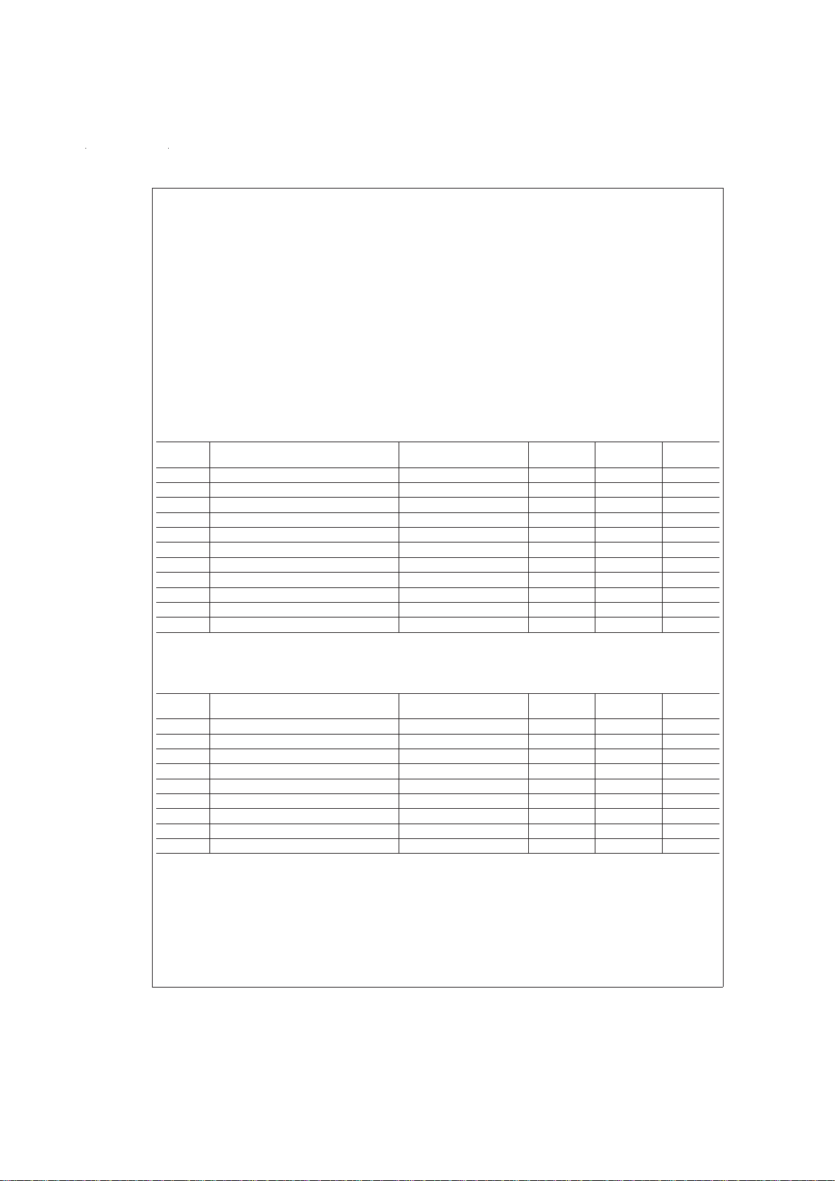
Test Circuit
DS012591-2
FIGURE 1. LM2202 Test Circuit
www.national.com3
Page 4
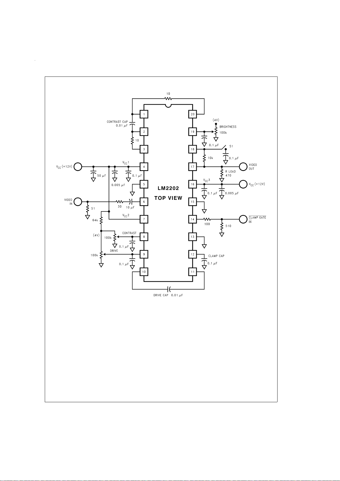
Typical Performance Characteristics (V
CC
=
12V, T
A
=
25˚C unless otherwise specified)
Circuit Description
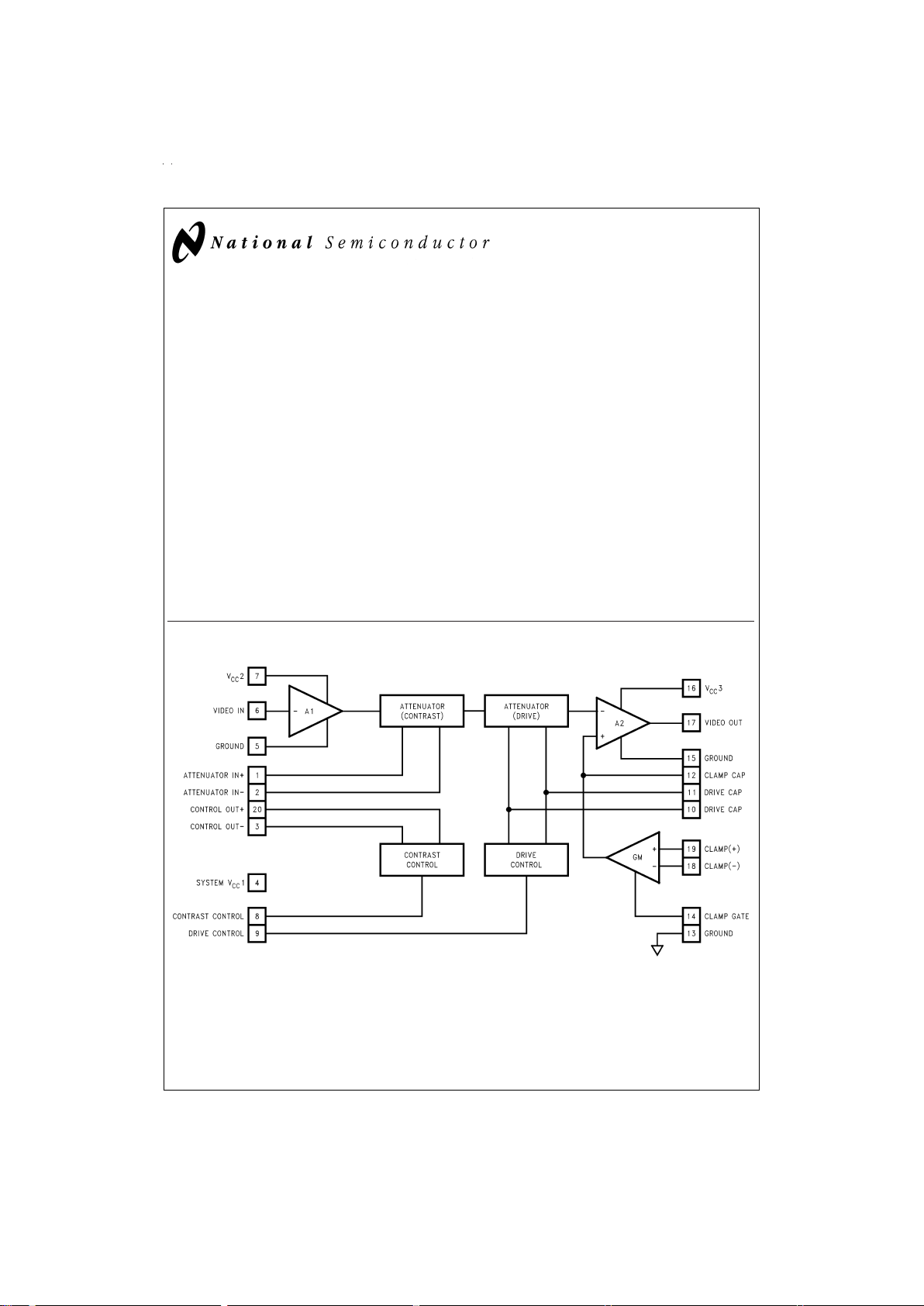
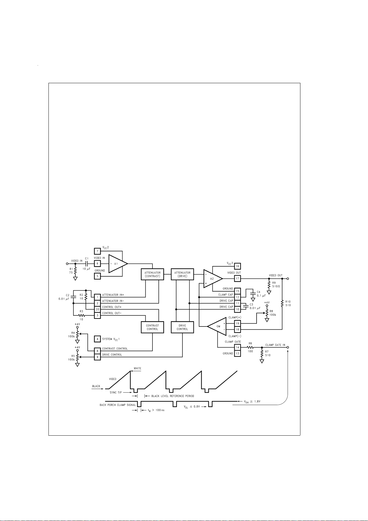
Figure 2
shows a block diagram of the LM2202 video amplifier along with contrast and brightness (black level) control.
Contrast control is a DC-operated attenuator which varies
the AC gain of the amplifier. Signal attenuation (contrast) is
achieved by varying the base drive to a differential pair and
thereby unbalancing the current through the differential pair.
As shown in
Figure 2
, pin 20 provides a 5.3V bias voltage for
the positive input of the attenuator (pin 1). Pin 3 provides a
control voltage for the negative input (pin 2) of the attenuator.
The voltage at pin 3 varies as the voltage at the contrast control input (pin 8) varies thus providing signal attenuation. The
gain is maximum (0 dB attenuation) if the voltage at pin 8 is
4V and is minimum (maximum attenuation) if the voltage at
pin 8 is 0V. The 0V to 4V DC-operated drive control at pin 9
Quiescent Supply Current
vs Supply Voltage
DS012591-3
Attenuation vs Drive Voltage
DS012591-4
Contrast vs Frequency
DS012591-5
Drive vs Frequency
DS012591-6
Attenuation vs
Contrast Voltage
DS012591-7
www.national.com 4
Page 5
Circuit Description (Continued)
providesa6dBgain adjustment range. This feature is necessary for RGB applications where independent gain adjustment of each channel is required.
The brightness or black level clamping requires a “sample
and hold” circuit which holds the DC bias of the video amplifier constant during the black level reference portion of the
video waveform. Black level clamping, often referred to as
DC restoration, is accomplished by applying a back porch
clamp signal to the clamp gate input pin (pin 14). The clamp
comparator is enabled when the clamp signal goes low during the black level reference period (see
Figure 2
). When the
clamp comparator is enabled, the clamp capacitor connected to pin 12 is either charged or discharged until the voltage at the minus input of the comparator matches the voltage set at the plus input of the comparator. During the video
portion of the signal, the clamp comparator is disabled and
the clamp capacitor holds the proper DC bias. In a DC
coupled cathode drive application, picture brightness function can be achieved by varying the voltage at the comparator’s plus input. Note that the back porch clamp pulse width
(t
W
in
Figure 2
) must be greater than 100 ns for proper op-
eration.
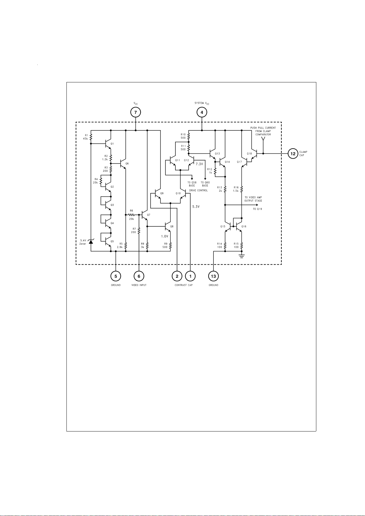
VIDEO AMPLIFIER SECTION (Input Stage)
A simplified schematic of LM2202’s video amplifier input
stage is shown in
Figure 3
. The 5.4V zener diode, Q1, Q6
and R2 bias the base of Q7 at 2.6V. The AC coupled video
signal applied to pin 6 is referenced to the 2.6V bias voltage.
Transistor Q7 buffers the video signal, V
IN
, and Q8 converts
the voltage to current. The AC collector current through Q8 is
I
C8
=
V
IN
/R9. Under maximum gain condition, transistors Q9
and Q11 are off and all of I
C8
flows through the load resistors
R10 and R11. The maximum signal gain at the base of Q13
is, A
V1
=
−(R10 + R11)/R9=−2. Signal attenuation is
achieved by varying the base drive to the differential pairs
Q9, Q10 and Q11, Q12 thereby unbalancing the collector
currents through the transistor pairs. Base of Q10 is biased
at 5.3V by externally connecting pin 1 to pin 20 through a
100Ω resistor. Pin 2 is connected to pin 3 through a 100Ω resistor.Adjustingthe contrast voltage at pin 8 produces a control voltage at pin 3 which drives the base of Q9. By varying
the voltage at the base of Q9, Q8’s collector current (I
C8
)is
diverted away from the load resistors R10 and R11, thereby
providing signal attenuation. Maximum attenuation is
achieved when all of I
C8
flows through Q9 and no current
flows through the load resistors.
The differential pair Q11 and Q12 provide drive control.
Q12’s base is internally biased at 7.3V.Adjusting the voltage
at the drive control input (pin 9) produces a control voltage at
the base of Q11. With Q9 off and Q12 off, all of I
C8
flows
through R10, thus providing a gain of A
V1
=
−(R10/R9) x V
IN
=
−1. Drive control thus provides a 6 dB attenuation range.
DS012591-8
FIGURE 2. Block Diagram of the LM2202 Video Amplifier
with Contrast and Brightness (Black Level) Control
www.national.com5
Page 6
Circuit Description (Continued)
VIDEO AMPLIFIER SECTION (Output Stage)
A simplified schematic of LM2202’s video amplifier output
stage is shown in
Figure 4
. The output stage is the second
gain stage. Ideally the gain of the second gain stage would
be A
V2
=
−R21/R18=−16. Because of the output stage’s
low open loop gain, the gain is approximately A
V2
=
−10.
Thus the maximum gain of the video amplifier is A
V
=
A
V1
x
A
V2
=
20. Transistors Q23 and Q24 provide a push-pull drive
to the load. The output voltage can swing from 0.2V to 10V.
CONTRAST CONTROL SECTION
A simplified schematic of LM2202’s contrast control section
is shown in
Figure 5
. A 0V to 4V DC voltage is applied at the
contrast input (pin 8). Transistors Q29, Q30 and Q34 buffer
and level shift the contrast voltage to the base of Q36. The
voltage at the emitter of Q36 equals the contrast voltage
(V
cont
) and the current through Q36’s collector is given by
I
C36
=
V
cont
/R28.
Transistor Q36’s collector current is used to unbalance the
current through the differential pair comprised of Q38 and
Q40. Q40’s base is internally biased at 5.3V and made avail-
able at pin 20. Pin 20 is externally connected to pin 1 through
a 100Ω resistor (see
Figure 2
and
Figure 3
). The base of
Q38 (pin 3) is externally connected to pin 2 through a 100Ω
resistor (see
Figure 2
and
Figure 3
). With V
cont
=
2V,the differential pair (Q38, Q40) is balanced and the voltage at pins
1 and 2 is 5.3V. Under this condition, Q8’s collector current is
equally split between Q9 and Q10 (see
Figure 3
) and the
amplifier’s gain is half the maximum gain. If contrast voltage
at pin 8 is greater than 2V then Q36’s collector current increases, thus pulling Q38’s collector node lower and consequently moving Q38’s base below 5.3V.With pin 2 at a lower
voltage than pin 1, current through Q10 (see
Figure 3
) in-
creases and the amplifier’s gain increases. With V
cont
=
4V,
the amplifier’s gain is maximum.
If the contrast voltage at pin 8 is less than 2V then Q36’s col-
lector current decreases and Q38’s base is pulled above
5.3V.With pin 2 voltage greater than pin 1 voltage, less current flows through Q10 (see
Figure 3
), consequently the am-
plifier’s gain decreases. With V
cont
=
0V,the amplifier’s gain
is minimum (i.e., maximum attenuation).
DS012591-9
FIGURE 3. Simplified Schematic of the LM2202 Video Amplifier Input Stage
www.national.com 6
Page 7

Circuit Description (Continued)
DS012591-10
FIGURE 4. Simplified Schematic of LM2202 Video Amplifier Output Stage
www.national.com7
Page 8

Circuit Description (Continued)
DS012591-11
FIGURE 5. Simplified Schematic of LM2202 Contrast Control
www.national.com 8
Page 9

Circuit Description (Continued)
DRIVE CONTROL SECTION
A simplified schematic of the LM2202’s drive control section
is shown in
Figure 6
. A 0V to 4V DC voltage is applied at the
drive control input (pin 9). Transistors Q49, Q50 and Q54
buffer and level shift the contrast voltage to the base of Q56.
The voltage at the emitter of Q56 equals the drive voltage,
V
drive
and the current through Q56’s collector is given by
I
C56
=
V
drive
/R43.
Transistor Q56’s collector current is used to unbalance the
current through the differential pair comprised of Q58 and
Q60. Q60’s base is internally biased at 7.3V and connected
to the base of Q12 (see
Figure 3
). Q58’s base is internally
connected to the base of Q11 (see
Figure 3
). With V
cont
=
2V, the differential pair (Q58, Q60) is balanced and the voltage at the bases of Q11 and Q12 is 7.3V. Under this condition, Q10’s collector current is equally split between Q11 and
Q12 (see
Figure 3
). If the drive voltage at pin 9 is greater
than 2V then Q56’s collector current increases, thus pulling
Q58’s collector node lower and consequently moving Q58’s
base below 7.3V. With base of Q11 below 7.3V, current
through Q12 (see
Figure 3
) increases and the amplifier’s
gain increases. With V
drive
=
4V,the amplifier’s gain is maxi-
mum under maximum contrast condition (i.e., V
cont
=
4V).
If the drive voltage at pin 8 is less than 2V then Q56’s collector current decreases and Q58’s base is pulled above 7.3V.
With base of Q11 greater than 7.3V, less current flows
through Q12 (see
Figure 3
), consequently the amplifier’s
gain decreases. With V
drive
=
0V,the amplifier’s gain is 6 dB
less than the maximum gain.
CLAMP GATE AND CLAMP COMPARATOR SECTION
Figure 7
and
Figure 8
show simplified schematics of the
clamp gate and clamp comparator circuits. The clamp gate
circuit (
Figure 7
) consists of a PNP input buffer transistor
(Q82), a PNP emitter coupled pair (Q85 and Q86) referenced on one side to 2.1V and an output switch transistor
Q89. When the clamp gate input at pin 14 is high (
>
1.5V)
the Q89 switch is on and shunts the 200 µAcurrent from current source Q90 to ground. When pin 14 is low (
<
1.3V) the
Q89 switch is off and the 200 µA current is mirrored by the
current mirror comprised of Q91 and Q75 (see
Figure 8
).
Consequently the clamp comparator comprised of the differential pair Q74 and Q77 is enabled. The input of the clamp
comparator is similar to the clamp gate except that an NPN
emitter coupled pair is used to control the current that will
charge or discharge the clamp capacitor externally connected from pin 12 to ground. PNP transistors are used at
the inputs because they offer a number of advantages over
NPNs. PNPs will operate with base voltages at or near
ground and will usually have a greater emitter base breakdown voltage (BVebo). Because the differential input voltage
to the clamp comparator during the video scan period could
be greater than the BVebo of NPN transistors, a resistor
(R63) with a value one half that of R60 or R68 is connected
between the bases of Q71 and Q79. The clamp comparator’s common mode range is from ground to approximately
9V and the maximum differential input voltage is V
CC
.
www.national.com9
Page 10

Circuit Description (Continued)
DS012591-12
FIGURE 6. Simplified Schematic of the LM2202 Drive Control
www.national.com 10
Page 11

Circuit Description (Continued)
DS012591-13
FIGURE 7. Simplified Schematic of the LM2202 Clamp Gate Circuit
www.national.com11
Page 12

Circuit Description (Continued)
Applications
SINGLE VIDEO CHANNEL
A typical application for a single video channel is shown in
Figure 9
. The video signal is AC coupled to pin 6. The
LM2202 internally biases the video signal to 2.6 V
DC
. Contrast control is achieved by applying a 0V to 4V DC voltage
at pin 8. The amplifier’s gain is minimum (i.e., maximum signal attenuation) if pin 8 is at 0V and is maximum if pin 8 is at
4V.With pin 9 (drive control) at 0V, the amplifier has a maximum gain of 10.
For DC restoration, a clamp signal must be applied to the
clamp gate input (pin 14). The clamp signal should be logic
low (less than 0.8V) only during the back porch (black level
reference period) interval (see
Figure 2
). The clamp gate input is TTL compatible. Brightness control is provided by applying a 0V to 4V DC voltage at pin 19. For example, if pin 19
is biased at 1V then the video signal’s black level will be
clamped at 1V. A 510Ω load resistor is connected from the
video output pin (pin 17) to ground. This resistor biases the
output stage of the amplifier. For power dissipation considerations, the load resistor should not be much less than 510Ω.
RGB VIDEO PREAMPLIFIER
Figure 10
shows an RGB video preamplifier circuit using
three LM2202s. Note that pins 1 and 2 of IC1 are connected
to pins 1 and 2 of IC2 and IC3 respectively.This allows IC1
to provide a master contrast control and optimum contrast
tracking. Adjusting the contrast voltage at pin 8 of IC1 will
vary the gain of all three video channels. Drive control input
(pin 9) of each LM2202 allows individual gain adjustment for
achieving white balance.
The black level of each video channel can be individually adjusted to the desired voltage by adjusting the voltage at pin
19. In a DC-coupled cathode drive application, adjusting the
voltage at pin 19 of each IC will provide cutoff adjustment. In
an AC-coupled cathode drive application, the video signal is
AC coupled and DC restored at the cathode. In such an application, the video signal’s black level may be clamped to
the desired level by simply biasing pin 19 to the black level
voltage by using a voltage divider at pin 19.
DS012591-14
FIGURE 8. Simplified Schematic of the LM2202 Clamp Comparator Circuit
www.national.com 12
Page 13

Applications (Continued)
DS012591-15
FIGURE 9. Typical LM2202 Application (Single Video Channel)
www.national.com13
Page 14

Applications (Continued)
DS012591-16
FIGURE 10. Typical RGB Application with Contrast, Drive and Black Level (Cutoff) Control
www.national.com 14
Page 15

Power Down Characteristics
The LM2202 includes a built-in power down spot killer to prevent a flash on the screen upon power down. The LM2202’s
output voltage decreases as the device is being powered
down, thus preventing a flash on the screen. In some preamplifiers, the video output signal may go high as the device is
being powered down. This may cause a whiter-than-white
level at the output of the CRT driver, thus causing a flash on
the screen.
PC Board Layout Considerations
For optimum performance and stable operation, a
double-sided printed circuit board with adequate ground
plane and power supply decoupling as close to the V
CC
pins
as possible is recommended. For suggestions on optimum
PC board layout, please see the reference section below.
Reference
Ott, Henry W,
Noise Reduction Techniques in Electronic
Systems
, John Wiley & Sons, New York, 1976.
www.national.com15
Page 16

Physical Dimensions inches (millimeters) unless otherwise noted
Order Number LM2202M
NS Package Number M20B
Order Number LM2202N
NS Package Number N20A
www.national.com 16
Page 17

Notes
LIFE SUPPORT POLICY
NATIONAL’S PRODUCTS ARE NOT AUTHORIZED FOR USE AS CRITICAL COMPONENTS IN LIFE SUPPORT
DEVICES OR SYSTEMS WITHOUT THE EXPRESS WRITTEN APPROVAL OF THE PRESIDENT AND GENERAL
COUNSEL OF NATIONAL SEMICONDUCTOR CORPORATION. As used herein:
1. Life support devices or systems are devices or
systems which, (a) are intended for surgical implant
into the body, or (b) support or sustain life, and
whose failure to perform when properly used in
accordance with instructions for use provided in the
labeling, can be reasonably expected to result in a
significant injury to the user.
2. A critical component is any component of a life
support device or system whose failure to perform
can be reasonably expected to cause the failure of
the life support device or system, or to affect its
safety or effectiveness.
National Semiconductor
Corporation
Americas
Tel: 1-800-272-9959
Fax: 1-800-737-7018
Email: support@nsc.com
National Semiconductor
Europe
Fax: +49 (0) 1 80-530 85 86
Email: europe.support@nsc.com
Deutsch Tel: +49 (0) 1 80-530 85 85
English Tel: +49 (0) 1 80-532 78 32
Français Tel: +49 (0) 1 80-532 93 58
Italiano Tel: +49 (0) 1 80-534 16 80
National Semiconductor
Asia Pacific Customer
Response Group
Tel: 65-2544466
Fax: 65-2504466
Email: sea.support@nsc.com
National Semiconductor
Japan Ltd.
Tel: 81-3-5639-7560
Fax: 81-3-5639-7507
www.national.com
LM2202 230 MHz Video Amplifier System
National does not assume any responsibility for use of any circuitry described, no circuit patent licenses are implied and National reserves the right at any time without notice to change said circuitry and specifications.
 Loading...