

Page 1
查询LM217M供应商
1.2 TO 37V ADJUSTABLE VOLTAGE REGULATOR
■ OUTPUTVOLTAGERANGE : 1.2 TO37V
■ OUTPUTCURRENT IN EXCESSOF 500 mA
■ LINEREGULATION TYP.0.01%
■ LOADREGULATIONTYP. 0.1%
■ THERMALOVERLOADPROTECTION
■ SHORTCIRCUIT PROTECTION
■ OUTPUTTRANSISTORSAFEAREA
COMPENSATION
■ FLOATINGOPERATIONFOR HIGH
VOLTAGEAPPLICATIONS
DESCRIPTION
The LM217M/LM317M are monolithic integrated
circuits in TO-220,DPAK, SOT-82 and SOT-194
packages intended for use as positive adjustable
voltageregulators.
They are designedto supply until 500 mAof load
current with an output voltage adjustable over a
1.2 to 37V range.
The nominal output voltage is selectedby means
of only a resistive divider, making the device
exceptionally easy to use and eliminating the
stockingof many fixed regulators.
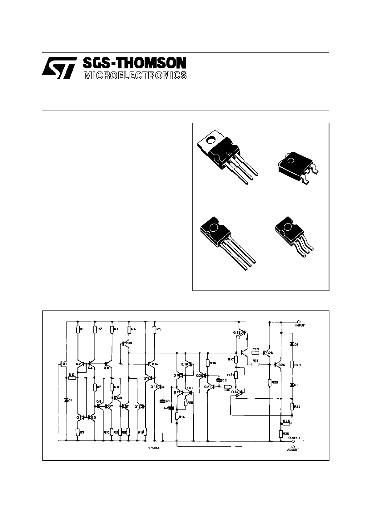
LM217M
LM317M
MEDIUM CURRENT
TO-220
SOT-82 SOT-194
DPAK
TO-252
SCHEMATICDIAGRAM
September 1997
1/11
Page 2
LM217M/LM317M
ABSOLUTE MAXIMUM RATINGS
Symbol Parameter Value Unit
V
T
(*) Re-Boot is not guaranteed for Tj≥ 85oC
THERMAL DATA
Symbol Parameter SOT-82
R
thj-case
R
thj-amb
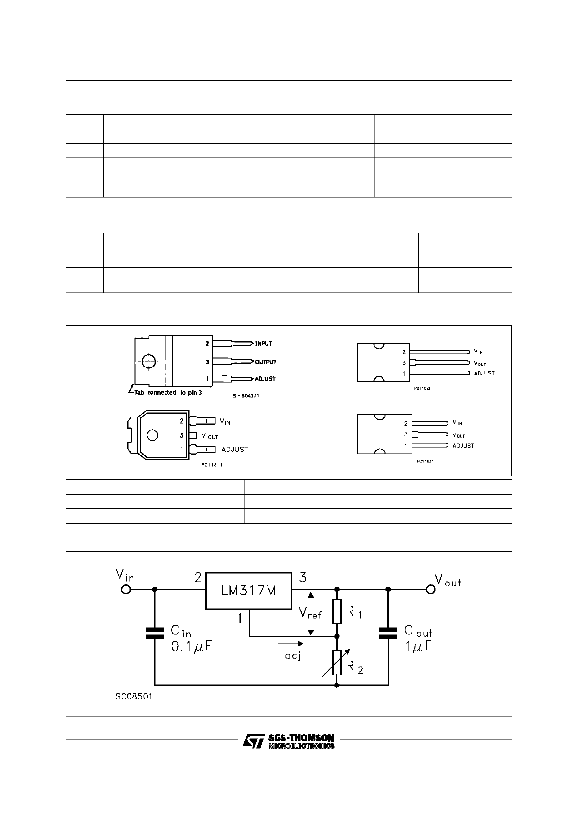
PINCONNECTION AND ORDERING NUMBERS
Input-Output Differential Voltage 40 V
i-Vo
P
Power Dissipation Internally Limited
d
Operating Junction Temperature Range (*) forLM217M
opr
forLM317M
T
StorageTemperature Range -55 to 150
stg
-40 to 125
0to125
TO-220 Unit
SOT-194
DPAK
ThermalResistance Junction-case Max
ThermalResistance Junction-ambient Max
8
100
TO-220 SOT-82
50
3
o
C/W
o
C/W
o
C
o
C
o
C
DPAK SOT-194
Type TO-220 DPAK SOT-82 SOT-194
LM217M LM217MT LM217 M DT LM217MX LM217 M S
LM317M LM317MT LM317 M DT LM317MX LM317 M S
TEST CIRCUIT
2/11
Page 3
LM217M/LM317M
ELECTRICALCHARACTERISTICS FOR LM217M (Refer to the test circuits, -40 ≤ Tj≤ 125oC
V
(*) CADJ is connected between Adjust pinand Ground.
= 5 V, Io= 100 mA, Pd≤ 7.5W, unlessotherwisespecified)
i-Vo
Symbol Parameter Test Conditions Min. Typ. Max. Unit
LineRegulation Vi-Vo= 3 to40 V Tj=25oC 0.01 0.02 %/V
∆V
o
0.02 0.05 %/V
LoadRegulation Vo≤ 5V
∆V
o
I
Adjustment Pin Current 50 100 µA
ADJ
∆I
V
I
o(min)
I
o(max)
Adjustment Pin Current Vi-Vo= 3 to40 V
ADJ
Reference Voltage Vi-Vo= 3 to40 V
REF
∆
V
OutputVoltage Temperature
o
Stability
V
o
Minimum LoadCurrent Vi-Vo=40V 3.5 5 mA
Maximum OutputCurrent Vi-Vo≤15V
OutputNoise Voltage
e
N
(percentance of V
)
O
SVR Supply Voltage Rejection (*) T
=10mA to 500 mA
I
o
≥ 5V
V
o
=10mA to 500 mA
I
o
=10mA to 500 mA
I
o
=10mA to 500 mA
I
o
=40V, Pd<P
V
i-Vo
B = 10Hzto 10KHz
Tj=25oC
=25oC
j
f = 120Hz
T
T
dMAX,Tj
C
=25oC515mV
j
20 50 mV
=25oC 0.1 0.3 % /V
j
0.3 1 %/V
0.2 5 µ A
1.2 1.25 1.3 V
0.7 %
500 1000
=25oC
200
0.003 %
C
=0 65 dB
ADJ
=10µF66 80 dB
ADJ
o
o
mA
ELECTRICALCHARACTERISTICS FOR LM317M (Refer to the test circuits, 0 ≤ Tj≤ 125oC
V
= 5 V, Io= 100 mA, Pd≤ 7.5W, unlessotherwisespecified)
i-Vo
Symbol Parameter Test Conditions Min. Typ. Max. Unit
LineRegulation Vi-Vo= 3 to40 V Tj=25oC 0.01 0.04 %/V
∆V
o
0.02 0.07 %/V
LoadRegulation Vo≤ 5V
∆V
o
I
Adjustment Pin Current 50 100 µA
ADJ
∆I
V
I
o(min)
I
o(max)
Adjustment Pin Current Vi-Vo= 3 to40 V
ADJ
ReferenceVoltage Vi-Vo= 3 to40 V
REF
∆
V
OutputVoltage Temperature
o
Stability
V
o
Minimum Load Current Vi-Vo=40V 3.5 10 mA
Maximum OutputCurrent Vi-Vo≤15V
OutputNoise Voltage
e
N
(percentance of V
)
O
SVR Supply Voltage Rejection (*) T
=10mA to 500 mA
I
o
≥ 5V
V
o
=10mA to 500 mA
I
o
=10mA to 500 mA
I
o
=10mA to 500 mA
I
o
=40V, Pd<P
V
i-Vo
B = 10Hzto 10KHz
Tj=25oC
=25oC
j
f = 120Hz
T
T
dMAX,Tj
C
=25oC525mV
j
20 70 mV
=25oC 0.1 0.5 % /V
j
0.3 1. 5 %/ V
0.2 5 µ A
1.2 1.25 1.3 V
0.7 %
500 1000
=25oC
200
0.003 %
C
=0 65 dB
ADJ
=10µF66 80 dB
ADJ
o
o
mA
(*) CADJ is connected between Adjust pinand Ground.
3/11
Page 4
LM217M/LM317M
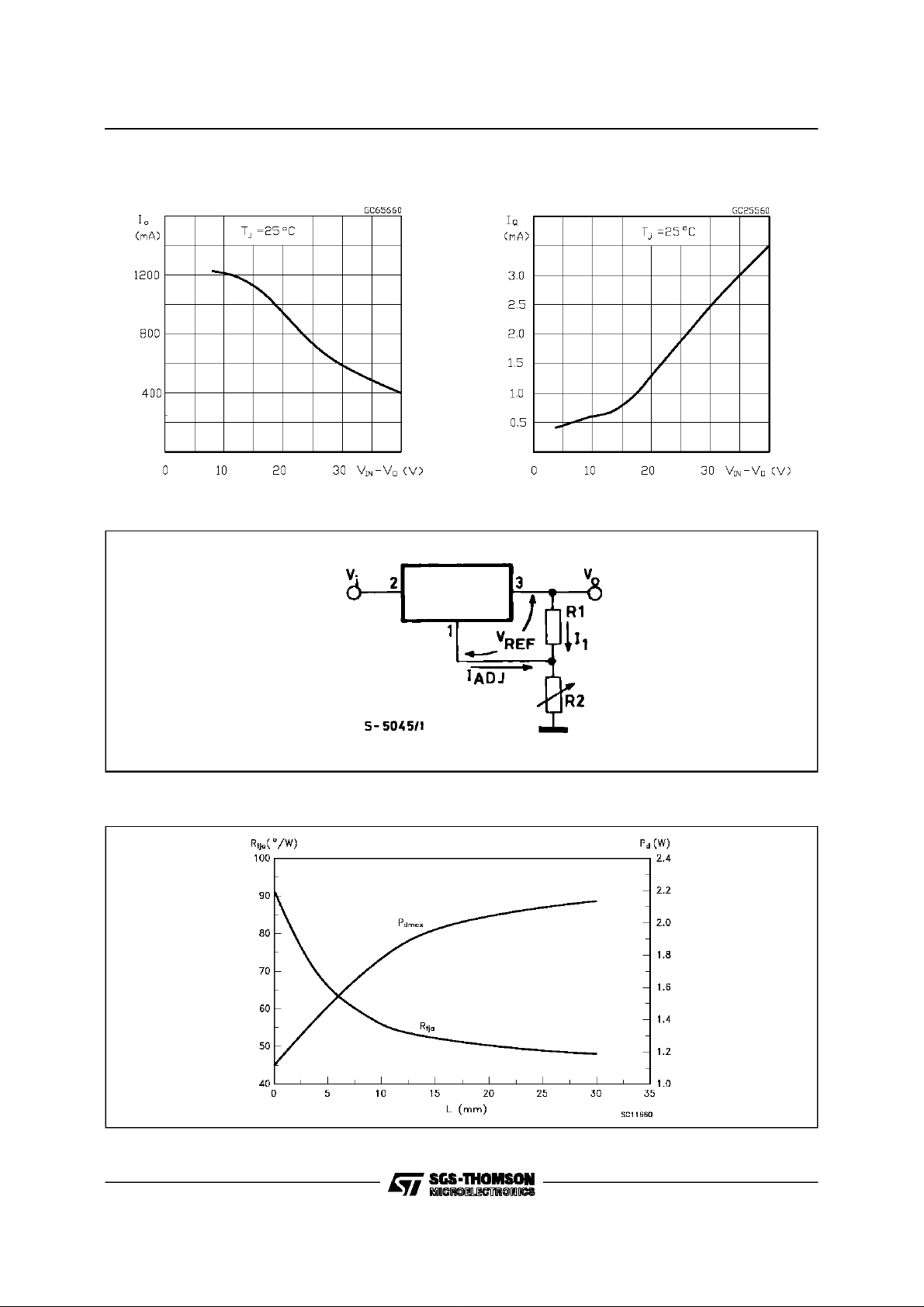
Figure1 : Current Limit Figure2 : MinimumOperatingCurrent
Figure3 : Basic AdjustableRegulator.
LM317M
Figure4 : ThermalResistance& MaximumPower Dissipationvs P.C.B. Copper Lenght for DPAK
Pdmax calculatedfor Ta=50oC
4/11
Page 5

LM217M/LM317M
APPLICATIONINFORMATION
The LM317M provides an internal reference
voltage of 1.25V between the output and
adjustments terminals. This is used to set a
constant current flow across an external resistor
divider(see fig. 3), giving an output voltageV
R
V
O=VREF
(1+
R
2
) +I
1
ADJR2
of:
O
The device was designed to minimize the term
(100µA max) and to maintain it very constant
I
ADJ
with line and load changes. Usually, the error
term IADJ⋅R2 can be neglected. To obtain the
previous requirement, all the regulator quiescent
current is returned to the output terminal,
imposinga minimum load current condition. If the
load is insufficient,the output voltagewill rise.
Since the LM317M is a floating regulator and
”sees” only the input-to-outputdifferential voltage,
supplies of very high voltage with respect to
ground can be regulatedas long as themaximum
input-to-output differential is not exceeded.
Furthermore, programmable regulator are easily
obtainable and, by connecting a fixed resistor
between the adjustment and output, the device
canbe usedas a precisioncurrent regulator.
In order to optimise the load regulation, the
current set resistor R1 (see fig. 3) should be tied
as close as possible to the regulator, while the
ground terminal of R2 should be near the ground
of the load to provide remote ground sensing.
EXTERNALCAPACITORS(Fig.5)
Normally no capacitors are needed unless the
device is situated far from the input filter
capacitors; in which case an input bypass is
needed.
A 0.1µF disc or 1µF tantalium input bypass
capacitor (C
) is recommended to reduce the
I
sensitivityto input line impedance.
The adjustment terminal may be bypassed to
ground to improve ripple rejection. This capacitor
) prevents ripple from being amplified as the
(C
adj
output voltage is increased. A 10µF capacitor
should improve ripple rejection about 80dB at
120Hzan a 10V application.
Although the LM317M is stable with no output
capacitance like any feedback circuit, certain
values of external capacitance can cause
excessive ringing. An output capacitance (C
O
)in
the form of a 1µF tantalium or 25µF aluminium
electrolytic capacitor on the output swamps this
effect andinsuresstability.
PROTECTIONDIODES (Fig.5)
When external capacitors are used with any IC
regulator it is sometimes necessary to add
protection diodes to prevent the capacitors from
discharging through low current points into the
regulator.
Figure 5 show the LM317M with the
recommended protection diodes for output
voltages in excess of 25V or high capacitance
values (C
prevents C
>25µF, C2>10µF). Diode D1
3
from discharging through the IC
3
during an input short-circuit. The combination of
diodes D1 and D2 prevents C
from discarging
2
through the regulator during an input or output
short-circuit.
START-UPBLOCK
It’s not guaranteed the Re-Boot of the device
when the junctiontemperatureis over 85
o
C.
5/11
Page 6

LM217M/LM317M
Figure5 : VoltageRegulatorwith ProtectionDiodes.
LM317M
Figure6 : Slow Turn-on 15V Regulator. Figure 7 : Current Regulator.
LM317M
LM317M
V
ref
I
=
o
+
R
1
I
ADJ
≈
1.25
R
V
1
Figure8 : 5V Electronic Shut-downRegulator. Figure9 : DigitallySelected Outputs.
LM317M
LM317M
(R2 sets maximum Vo)
6/11
Page 7

TO-220 MECHANICALDATA
LM217M/LM317M
DIM.
MIN. TYP. MAX. MIN. TYP. MAX.
A 4.8 0.189
C 1.37 0.054
D 2.4 2.8 0.094 0.110
D1 1.2 1.35 0.047 0.053
E 0.35 0.55 0.014 0.022
F 0.61 0.94 0.024 0.037
F2 1.15 1.4 0.045 0.055
G 4.95 5.08 5.21 0.195 0.200 0.205
H2 10.4 0.409
H3 10.05 10.4 0.396 0.409
L2 16.2 0.638
L3 26.3 26.7 27.1 1.035 1.051 1.067
L5 2.6 3 0.102 0.118
L6 15.1 15.8 0.594 0.622
L7 6 6.6 0.236 0.260
Dia. 3.65 3.85 0.144 0.152
mm inch
P011D
7/11
Page 8

LM217M/LM317M
TO-252 (DPAK) MECHANICAL DATA
DIM.
mm inch
MIN. TYP. MAX. MIN. TYP. MAX.
A 2.2 2.4 0.086 0.094
A1 0.9 1.1 0.035 0.043
A2 0.03 0.23 0.001 0.009
B 0.64 0.9 0.025 0.035
B2 5.2 5.4 0.204 0.212
C 0.45 0.6 0.017 0.023
C2 0.48 0.6 0.019 0.023
D 6 6.2 0.236 0.244
E 6.4 6.6 0.252 0.260
G 4.4 4.6 0.173 0.181
H 9.35 10.1 0.368 0.397
L2 0.8 0.031
L4 0.6 1 0.023 0.039
8/11
H
A
E
C2
L2
B2
==
==
DETAIL”A”
D
2
13
L4
A1
C
A2
DETAIL”A”
B
G
==
0068772-B
Page 9

SOT-82 MECHANICAL DATA
LM217M/LM317M
DIM.
MIN. TYP. MAX. MIN. TYP. MAX.
A 7.4 7.8 0.291 0.307
B 10.5 11.3 0.413 0.445
b 0.7 0.9 0.028 0.035
b1 0.49 0.75 0.019 0.030
C 2.4 2.7 0.04 0.106
c1 1.2 0.047
D 15.7 0.618
e 2.2 0.087
e3 4.4 0.173
F 3.8 0.150
H 2.54 0.100
mm inch
C
c1
b
b1
A
F
BD
H
e
e3
P032A
9/11
Page 10

LM217M/LM317M
SOT-194 MECHANICAL DATA
DIM.
MIN. TYP. MAX. MIN. TYP. MAX.
A 7.4 7.8 0.291 0.307
B 10.5 11.3 0.413 0.445
b 0.7 0.9 0.028 0.035
b1 0.49 0.75 0.019 0.030
C 2.4 2.7 0.094 0.106
c1 1.2 0.047
c2 1.3 0.051
D 6 0.236
e 2.2 0.087
e3 4.4 0.173
F 3.8 0.150
H 2.54 0.100
P 45 (typ.)
S 4 0.157
S1 2 0.079
T 0.1 0.004
mm inch
C
A
F
B
C1
H
D
b1
T
e
SS1
P
b
c2
e3
P032B
10/11
Page 11

LM217M/LM317M
Information furnished is believed tobe accurateand reliable.However, SGS-THOMSONMicroelectronicsassumes no responsabilityfor the
consequences of use ofsuch informationnor for anyinfringement of patents or other rights of thirdparties whichmay results from its use. No
licenseis granted by implicationor otherwise underany patentorpatentrights ofSGS-THOMSON Microelectronics.Specifications mentioned
in this publication are subject tochange withoutnotice. This publication supersedesand replaces all informationpreviouslysupplied.
SGS-THOMSONMicroelectronicsproducts arenotauthorizedfor use ascriticalcomponents inlife support devices orsystemswithoutexpress
writtenapproval ofSGS-THOMSON Microelectonics.
1997 SGS-THOMSONMicroelectronics- Printedin Italy - AllRights Reserved
Australia- Brazil- Canada - China - France- Germany - Hong Kong- Italy -Japan - Korea- Malaysia - Malta - Morocco- The Netherlands -
Singapore- Spain - Sweden - Switzerland- Taiwan- Thailand- United Kingdom- U.S.A
SGS-THOMSONMicroelectronics GROUPOF COMPANIES
.
11/11
 Loading...