

Page 1
( ) Preliminary Specification
( ● ) Final Specification
LM215WF3
Liquid Crystal Display
Product Specification
SPECIFICATION
FOR
APPROVAL
21.5” Full HD TFT LCDTitle
BUYER
www.jxlcd.com
www.jxlcd.com
APPROVED BY
/
/
/
APPLE
K60MODEL
SIGNATURE
DATE
SUPPLIER LG Display Co., Ltd.
*MODEL LM215WF3
SUFFIX SDC2
*When you obtain standard approval,
please use the above model name without suffix
APPROVED BY
S. Y. Park / G.Manager
REVIEWED BY
D. Y. KIM / Manager [C]
D. Y. KIM/ Manager [M]
S. H. Cho / Manager [P]
PREPARED BY
Y. T. YOO / Engineer
SIGNATURE
DATE
Please return 1 copy for your confirmation with
your signature and comments.
Ver. 1.0 January. 13 . 2011
MNT Products Engineering Dept.
LG Display Co., Ltd
1 / 35
Page 2
LM215WF3
Liquid Crystal Display
Product Specification
Contents
No ITEM Page
COVER
CONTENTS
RECORD OF REVISIONS
1 GENERAL DESCRIPTION
2 ABSOLUTE MAXIMUM RATINGS
3 ELECTRICAL SPECIFICATIONS
3-1 ELECTRICAL CHARACTREISTICS
3-2 INTERFACE CONNECTIONS
3-3 SIGNAL TIMING SPECIFICATIONS
3-4 SIGNAL TIMING WAVEFORMS
3-5 COLOR INPUT DATA REFERNECE
3-6 POWER SEQUENCE
4 OPTICAL SFECIFICATIONS
5 MECHANICAL CHARACTERISTICS
6 RELIABLITY
www.jxlcd.com
www.jxlcd.com
1
2
4
5
6
7
7
9
12
13
14
15
18
24
27
7 INTERNATIONAL STANDARDS
7-1 SAFETY
7-2 EMC
7-3 ENVIRONMENT
8 PACKING
8-1 DESIGNATION OF LOT MARK
8-2 PACKING FORM
9 PRECAUTIONS 30
9-1 MOUNTING PRECAUTIONS 30
9-2 OPERATING PRECAUTIONS 30
9-3 ELECTROSTATIC DISCHARGE CONTROL 31
9-4 PRECAUTIONS FOR STRONG LIGHT EXPOSURE 31
9-5 STORAGE 31
9-6 HANDLING PRECAUTIONS FOR PROTECTION FILM 31
Ver. 1.0 January. 13 . 2011
28
28
28
28
29
29
29
2 / 35
Page 3
LM215WF3
Liquid Crystal Display
Product Specification
Contents
No ITEM Page
10 EDID DATA 32
10-1 EDID DATA 32
10-2 EDID READ/WRITE PROTOCOL 35
www.jxlcd.com
www.jxlcd.com
Ver. 1.0 January. 13 . 2011
3 / 35
Page 4
Product Specification
RECORD OF REVISIONS
LM215WF3
Liquid Crystal Display
Revision
No
0.0 Sep.15 . 2010 - First Draft (Preliminary)
1.0 Jan.13 . 2011 32~35 Update EDID
Revision Date Page Description
www.jxlcd.com
www.jxlcd.com
Ver. 1.0 January. 13 . 2011
4 / 35
Page 5
LM215WF3
Liquid Crystal Display
Product Specification
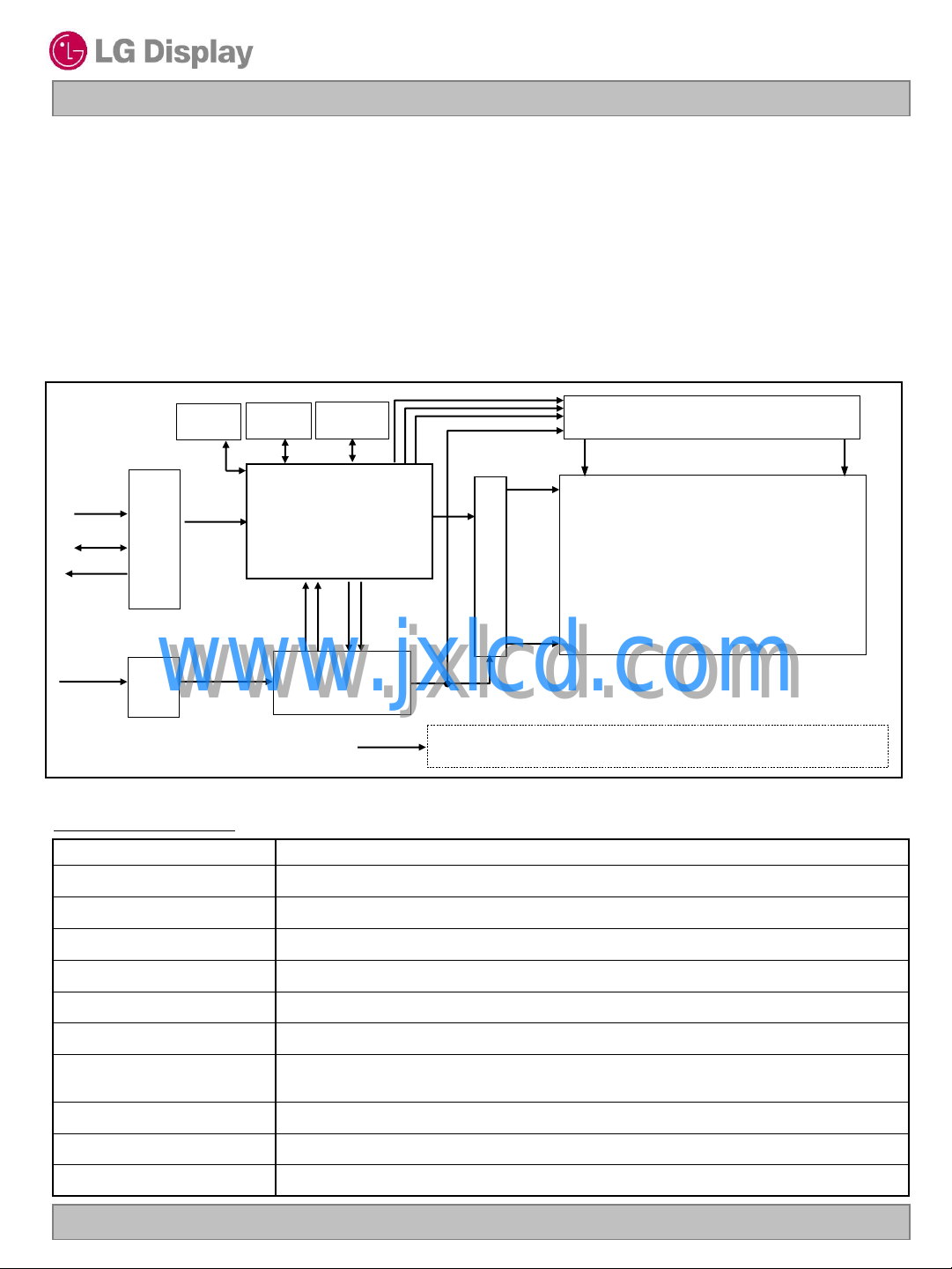
1. General Description
LM215WF3 is a Color Active Matrix Liquid Crystal Display with Light Emitting Diode ( White LED) backlight
system without LED driver. The matrix employs a-Si Thin Film Transistor as the active element.
It is a transmissive type display operating in the normally black mode. It has a 21.5inch diagonally
measured active display area with Full HD resolution (1920 vertical by 1080 horizontal pixel array)
Each pixel is divided into Red, Green and Blue sub-pixels or dots which are arranged in vertical stripes.
Gray scale or the brightness of the sub-pixel color is determined with a 8bit gray scale signal for each dot,
th u s, pr ese nt in g a p a le tt e of mo r e t ha n 16M co lor s. .
It has been designed to apply the 8bit 4Lane Display port interface.
It is in te nd ed to s up po rt di spl ay s wh er e h i g h b ri gh t n e s s , s u pe r w id e vi ew in g a ng le,
high color saturation, and high color are important.
RGB
Flash
Memory
SPI
Logic Power
3.3V / 1.2V
EEPROM
I2C
Timing
Controller
Power
Enable
(Video On)
Source Driver Circuit
S1 S1920
G1
Gate Driver Circuit
TFT - LCD Panel
(1920 × RGB × 1080 pixels)
G1080
Main Link
4 Lane
AUX CH
HPD
EEPROM
(LUT)
I2C
CN1
(30pin)
LCD Power
12 V
CN2
www.jxlcd.com
www.jxlcd.com
(6pin)
Power Circuit
Block
VLED 2ch
[ Figure 1 ] Block diagram
B/L System (White LED)
General Features
Active Screen Size 21.46 inches(545.22mm) diagonal
Outline Dimension 495.6(H) x 305.25(V) x 14.8(D) mm(Typ.)
Pixel Pitch 0.2475mm x 0.2475mm
Pixel Format 1920 horiz. By 1080 vert. Pixels RGB stripes arrangement
Color Depth 8-bit, 16,777,216 colors
Luminance, White 365 cd/m
Viewing Angle(CR>10) View Angle Free (R/L 178(Typ.), U/D 178(Typ.))
Power Consumption
Weight 2100g (typ.)
Display Operating Mode Transmissive mode, normally black
Surface Treatment Hard coating(2H), Glare (Low Reflection treatment of the front polarizer)
Total 46.7 Watt (Max.)
(7.5 Watt @VLCD, Max 39.2 Watt_ Duty 100% of DC 350 mA_ w/o driver)
2
( 5point Avg.)
Ver. 1.0 January. 13 . 2011
5 / 35
Page 6
LM215WF3
Liquid Crystal Display
Product Specification
2. Absolute Maximum Ratings
The following are maximum values which, if exceeded, may cause faulty operation or damage to the unit.
Table 1. ABSOLUTE MAXIMUM RATINGS
Parameter Symbol
Power Input Voltage
Operating Temperature
Storage Temperature
Operating Ambient Humidity
Storage Humidity
Note.
1. Temperature and relative humidity range are shown in the figure below.
Wet bulb temperature should be 39 °C Max, and no condensation of water.
2. Storage condition is guaranteed under packing condition.
www.jxlcd.com
www.jxlcd.com
Wet Bulb
Temperature [C]
10
0
VLCD -0.3 14 Vdc at 25 2°C
TOP 0 50
TST -20 60
HOP 10 90 %RH
HST 10 90 %RH
50
40
30
20
Values
Min Max
90%
60
60%
40%
Humidity [(%)RH]
10%
Units Notes
°C
°C
1
Storage
Operation
10 20 30 40 50 60 70 800-20
Dry Bulb Temperature [C]
[ Figure 2 ] Temperature and relative humidity
Ver. 1.0 January. 13 . 2011
6 / 35
Page 7

LM215WF3
Liquid Crystal Display
Product Specification
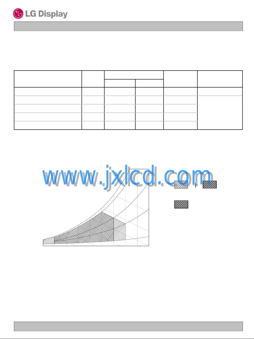
3. Electrical Specifications
3-1. Electrical Characteristics
It requires two power inputs. One is employed to power the LCD electronics and to drive the TFT array and
liquid crystal. The second input power for the WLED.
Table 2-1. ELECTRICAL CHARACTERISTICS
Parameter Symbol
MODULE :
Power Supply Input Voltage VLCD 11.4 12.0 12.6 Vdc
Permissive Power Input Ripple VRF - - 400 mV
Power Supply Input Current ILCD
Power Consumption
Rush current IRUSH - - 3.0 A 3
Note.
1. The specified current and power consumption are under the V
2. The current is specified at the maximum current pattern.
3. The duration of rush current is about 2ms and rising time of power Input is 1ms(min.)
www.jxlcd.com
www.jxlcd.com
whereas mosaic pattern(8 x 6) is displayed and fVis the frame frequency.
White : 255Gray
Black : 0Gray
PLCD 4.64 5.57 Watt 1
PLCD 6.24 7.50 Watt 2
Min Typ Max
310 387 464 mA 1
416 520 624 mA 2
Values
=12.0V, 25 2°C,fV=60Hz condition
LCD
Maximum current pattern
Unit Notes
Mosaic Pattern(8 x 6)
Ver. 1.0 January. 13 . 2011
White Pattern
7 / 35
Page 8
Product Specification
Table 2-2. LED Bar ELECTRICAL CHARACTERISTICS
LM215WF3
Liquid Crystal Display
Items Symbol
LED String Voltage V
LED String Power P
BL Power P
LED Life Time LED_LT 30K - Hrs
LED Junction Temperature Tj 150
LED driver design guide
: The design of the LED driver must have specifications for the LED in LCD Assembly.
The performance of the LED in LCM, for example life time or brightness, is extremely influenced by
the characteristics of the LED driver.
So all the parameters of an LED driver should be carefully designed and output current should be
Constant current control.
Please control feedback current of each string individually to compensate the current variation
among the strings of LEDs.
When you design or order the LED driver, please make sure unwanted lighting caused by
the mismatch of the LED and the LED driver (no lighting, flicker, etc) never occurs.
When you confirm it, the LCD module should be operated in the same condition as installed in
your instrument.
www.jxlcd.com
www.jxlcd.com
S
S
BL
Min Typ Max
49.6 52.8 56.0 Vrms
17.36 18.48 19.60 W
- 36.96 39.2 W
Spec
Unit Remark Notes
1,2,3,
7
1,2,3,
4,6,7
1,2,4,
6,7
5,7,8
℃
Ta=25℃, at Duty 100%
of DC 350mA
Ta=25℃, at Duty 100%
of DC 350mA
Ta=25℃, at Duty 100%
of DC 350mA
Tj≤90℃, at Duty 100%
of DC 350mA
- 7,8
1. Specified values are for a single LED bar.
2. The specified current is input LED chip 100% duty current.
3. The specified voltage is input LED string and Bar voltage at typical 350mA 100% duty current.
4. The specified power consumption is input LED bar power consumption at typical 350mA 100% duty current.
5. The LED life time is determined as the time at which brightness of the LED is 70% compared to that of initial
value at the typical LED current on condition of continuous operating at below junction temperature 90°C.
6. The LED power consumption shown above does not include loss of external driver.
The used LED BL current is the LED typical current.
String Power Consumption is calculated with PS= VSx 350mA
BL Power Consumption is calculated with PBL= VSx 350mA x 2(string no.)
7. LED operating DC Forward Current and Junction Temperature must not exceed LED Max Ratings.
8. The LED life time and the maximum rating of LED junction temperature are evaluated at LED package level,
not at liquid crystal module level.
Ver. 1.0 January. 13 . 2011
8 / 35
Page 9
LM215WF3
Liquid Crystal Display
Product Specification
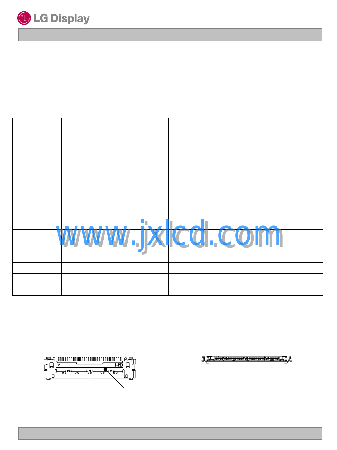
3-2. Interface Connections
3-2-1. LCD Module
- LCD Connector(CN1) : 20525-030E-01 (I-PEX) or Equivalent
Table 3. MODULE CONNECTOR(CN1) PIN CONFIGURATION
No Symbol Description No Symbol Description
1
2
3
4
5
6
7
8
GND
DDC_SDA
DDC_SCL
GND
I2C_SDA
I2C_SCL
GND
SPDIF
High Speed Ground 16
DDC Data 17
DDC Clock 18 Lane1P
High Speed Ground 19 Lane1N
DDC Data 20
DDC Clock 21 Lane2P
High Speed Ground 22 Lane2N
Audio output from DP RX
23
Lane0N
GND
GND
GND
Component Signal for Main Link 0
High Speed Ground
True Signal for Main Link 1
Component Signal for Main Link 1
High Speed Ground
True Signal for Main Link 2
Component Signal for Main Link 2
High Speed Ground
OPTION-1
9
10
11
12
13
14
15
Note: 1. All GND(ground) pins should be connected together and to Vss which should also be connected to
HPD
GND
AUX_CHN Component Signal for Auxiliary Channel
AUX_CHP True Signal for Auxiliary Channel
GND
Lane0P
the LCD’s metal frame.
Logic (N.C)
Hot Plug Detect Signal
www.jxlcd.com
www.jxlcd.com
High Speed Ground 26
High Speed Ground 29 VSYNC
True Signal for Main Link 0 30
1
20525-030E-01 (I-PEX)
30
24 Lane3P True Signal for Main Link 3
25 Lane3N
GND
27 VIDEO_ON
28 OPTION-2
GND
Component Signal for Main Link 3
High Speed Ground
Video status from DP RX
Logic (N.C)
Vertical Frame Sync.
High Speed Ground
#1
Rear view of LCM
#30
[ Figure 3 ] User Connector diagram
Ver. 1.0 January. 13 . 2011
9 / 35
Page 10
Product Specification
3-2-2. User Connector
- LCD Connector(CN2) : 53780-8606 (Manufactured by Molex) or Equivalent
Table 4. LCM POWER CONNECTOR(CN2) PIN CONFIGURATION
Pin Symbol Description NOTES
LM215WF3
Liquid Crystal Display
1 GND
2 GND
3 GND
4 VLCD 12V for LCM main power
5
6
Note : 1) NC : No Connection
#1 #6
www.jxlcd.com
www.jxlcd.com
VLCD 12V for LCM main power
VLCD 12V for LCM main power
53780-8606
[ Figure 3-1 ] User Connector diagram
GROUND
GROUND
GROUND
#1 #6
Rear view of LCM
- LCD Connector(CN6) : 53780-8604 (Manufactured by Molex) or Equivalent
Table 4-1. Thermal sensor CONNECTOR(CN6) PIN CONFIGURATION
Pin Symbol Description NOTES
1 DXP Positive connection to remote temperature sensor.
2 DXN Negative connection to remote temperature sensor.
3 GND Ground
4 VSYNCM VSYNCM for synchronized LED Driver
Ver. 1.0 January. 13 . 2011
10 / 35
Page 11

Product Specification
3-2-3. Backlight Interface
Driver connector: H401K-D06N-12B (Manufactured by E&T)
Mating Connector: 4530K-F06N-01R (Manufactured by E&T)
Table 5. LED DRIVER CONNECTOR PIN CONFIGURATION
Pin Symbol Description NOTES
LM215WF3
Liquid Crystal Display
1
2
3
4
5
6
www.jxlcd.com
www.jxlcd.com
LED1-
LED2+
NC
LED1+
LED2-
NC
LED channel 1 cathode – Left bar
LED channel 2 Anode – Left bar
NC
LED channel 1 Anode – Right bar
LED channel 2 cathode – Right bar
NC
NC/ 2- / 1+/ NC/ 2+ /1
6
1
To right side
[ Figure 4 ] LED Driver Connector Pin
Ver. 1.0 January. 13 . 2011
To left side
11 / 35
Page 12

LM215WF3
Liquid Crystal Display
Product Specification
3-3. Signal Timing Specifications
All of the interface signal timing should be satisfied with the following specifications for it‟s proper operation.
Table 6. TIMING TABLE
ITEM Symbol Min Typ Max Unit Note
DCLK
Horizontal
Vertical
Note: Hsync period and Hsync width-active should be even number times of tCLK. If the value
is odd number times of tCLK, display control signal can be asynchronous. In order to operate
this LCM a Hsync, Vsync, and DE(data enable) signals should be used.
1. The performance of the electro-optical characteristics may be influenced by variance of the
vertical refresh rates.
2. Vsync and Hsync should be keep the above specification.
3. Hsync Period, Hsync Width, and Horizontal Back Porch should by any times of character
number(8).
4. The polarity of Hsync, Vsync is not restricted.
Period tCLK - 7.22 - ns
Frequency - - 138.5 - MHz
total tHP - 2080 - tCLK
Frequency fH - 66.59 -
Blanking - 160 - tCLK
valid tWH - 1920 - tCLK/2
total tVP - 1111 - tHP
Frequency fV - 60 - Hz
Blanking - 31 - tHP
valid tWV - 1080 - tHP
www.jxlcd.com
www.jxlcd.com
KHz
Ver. 1.0 January. 13 . 2011
12 / 35
Page 13

3-4. Signal Timing Waveforms
1. DCLK , DE, DATA waveforms
t
CLK
Dclk
t
SD
Invalid
Data
DE(Data Enable)
t
SI
Product Specification
t
HD
Valid
LM215WF3
Liquid Crystal Display
Invalid
t
HI
2. Horizontal waveform
www.jxlcd.com
www.jxlcd.com
DE(Data Enable)
3. Vertical waveform
DE(Data Enable)
tHP
tHV
tVV
tHP
t
DE
VP
DE
Ver. 1.0 January. 13 . 2011
13 / 35
Page 14

LM215WF3
Liquid Crystal Display
Product Specification
3-5. Color Input Data Reference
The Brightness of each primary color(red,green,blue) is based on the 8-bit gray scale data input for the color;
the higher the binary input, the brighter the color. The table below provides a reference for color versus data
input.
Table 7. COLOR DATA REFERENCE
Input Color Data
Basic
Color
RED
Color
Black 0 0 0 0 0 0 0 0 0 0 0 0 0 0 0 0 0 0 0 0 0 0 0 0
Red (255) 1 1 1 1 1 1 1 1 0 0 0 0 0 0 0 0 0 0 0 0 0 0 0 0
Green (255) 0 0 0 0 0 0 0 0 1 1 1 1 1 1 1 1 0 0 0 0 0 0 0 0
Blue (255) 0 0 0 0 0 0 0 0 0 0 0 0 0 0 0 0 1 1 1 1 1 1 1 1
Cyan 0 0 0 0 0 0 0 0 1 1 1 1 1 1 1 1 1 1 1 1 1 1 1 1
Magenta 1 1 1 1 1 1 1 1 0 0 0 0 0 0 0 0 1 1 1 1 1 1 1 1
Yellow 1 1 1 1 1 1 1 1 1 1 1 1 1 1 1 1 0 0 0 0 0 0 0 0
White 1 1 1 1 1 1 1 1 1 1 1 1 1 1 1 1 1 1 1 1 1 1 1 1
www.jxlcd.com
RED (000) Dark 0 0 0 0 0 0 0 0 0 0 0 0 0 0 0 0 0 0 0 0 0 0 0 0
www.jxlcd.com
RED (001) 0 0 0 0 0 0 0 1 0 0 0 0 0 0 0 0 0 0 0 0 0 0 0 0
... ... ... ...
RED (254) 1 1 1 1 1 1 1 0 0 0 0 0 0 0 0 0 0 0 0 0 0 0 0 0
RED (255) 1 1 1 1 1 1 1 1 0 0 0 0 0 0 0 0 0 0 0 0 0 0 0 0
GREEN (000) Dark 0 0 0 0 0 0 0 0 0 0 0 0 0 0 0 0 0 0 0 0 0 0 0 0
MSB LSB
R7 R6 R5 R4 R3 R2 R1 R0 G7 G 6 G5 G4 G3 G 2 G1 G0 B7 B 6 B 5 B 4 B 3 B2 B 1 B 0
RED
MSB LSB
GREEN
BLUE
MSB LSB
GREEN (001) 0 0 0 0 0 0 0 0 0 0 0 0 0 0 0 1 0 0 0 0 0 0 0 0
GREEN
GREEN (254) 0 0 0 0 0 0 0 0 1 1 1 1 1 1 1 0 0 0 0 0 0 0 0 0
GREEN (255) 0 0 0 0 0 0 0 0 1 1 1 1 1 1 1 1 0 0 0 0 0 0 0 0
BLUE (000) Dark 0 0 0 0 0 0 0 0 0 0 0 0 0 0 0 0 0 0 0 0 0 0 0 0
BLUE (001) 0 0 0 0 0 0 0 0 0 0 0 0 0 0 0 0 0 0 0 0 0 0 0 1
BLUE
BLUE (254) 0 0 0 0 0 0 0 0 0 0 0 0 0 0 0 0 1 1 1 1 1 1 1 0
BLUE (255) 0 0 0 0 0 0 0 0 0 0 0 0 0 0 0 0 1 1 1 1 1 1 1 1
Ver. 1.0 January. 13 . 2011
... ... ... ...
... ... ... ...
14 / 35
Page 15

3-6. Power Sequence
3-6-1. Power Sequence
LM215WF3
Liquid Crystal Display
Product Specification
www.jxlcd.com
www.jxlcd.com
200
Notes : [1] HPD is asserted high by Sink at power-up
[2] SYMBOL_LOCK indicated by contents of Sink DPCD registers 00202h to 00205h
[3] VIDEO_ON asserted high by Sink when video to panel is valid
[6] BL_EN is an active-high MLB enable signal for panel BLU
Notes : 1. Please avoid floating state of interface signal at invalid period.
2. When the interface signal is invalid, be sure to pull down the power supply for LCD V
3. LED power must be turn on after power supply for LCD and interface signal are valid.
LCD
to 0V.
Ver. 1.0 January. 13 . 2011
15 / 35
Page 16

Product Specification
LM215WF3
Liquid Crystal Display
www.jxlcd.com
www.jxlcd.com
Notes : [2] SYMBOL_LOCK indicated by contents of Sink DPCD registers 00202h to 00205h
[4] Power-state set by Source in Sink DPCD register 00600h
[5] VIDEO_ON asserted low by Sink because of :
1) loss of SYMBOL_LOCK or
2) DP Sink is powered down
[7] BL_EN must be asserted low by system as rapidly as possible when video is invalid
to avoid visible artifacts
[8] T14 defines minimum off-time for 12V power
[9] min. times of 0 indicate precedence ordering of events, e.g. where actual timing is TBD
Ver. 1.0 January. 13 . 2011
16 / 35
Page 17

3-6-2. State Machine
LM215WF3
Liquid Crystal Display
Product Specification
OFF MODE
NEGATIVE
DC STATE
(OR CABLE
UNPLUG)
www.jxlcd.com
www.jxlcd.com
SOURCE
WRITES
02
SLEEP MODE
DP AUX
CHANNEL
NEGATIVE
LINE
DPCD
0x600
VALUE
POSITIVE
DC STATE
SOURCE
WRITES
01
ON MODE
Ver. 1.0 January. 13 . 2011
17 / 35
Page 18

LM215WF3
Liquid Crystal Display
Product Specification
4. Optical Specifications
Optical characteristics are determined after the unit has been „ON‟ for approximately 70 minutes
in a dark environment at 25±2°C. The values specified are at an approximate distance 50cm from the LCD
surface at a viewing angle of and equal to 0 ° and aperture 1 degree.
FIG. 8 presents additional information concerning the measurement equipment and method.
Pritchard 880 or
equivalent
Optical Stage(x,y)
LCD Module
50cm
[ Figure 5 ] Optical characteristic measurement equipment and method
Table 8. OPTICAL CHARACTERISTICS
Parameter Symbol
Contrast Ratio CR 700 1000 - 1
Surface Luminance, white L
Luminance Variation
Response Time
Color Coordinates
[CIE1931]
Color Shift
Viewing Angle (CR>10)
General
Effective
Gray Scale 2.2 8
www.jxlcd.com
www.jxlcd.com
Horizontal
Vertical
Horizontal
Vertical
Rise Time Tr
Decay Time Tr
RED Rx
GREEN Gx 0.301
BLUE Bx 0.147
WHITE Wx 0.313
Horizontal
Vertical
WH
WHITE
R
D
Ry 0.332
Gy 0.618
By 0.048
Wy 0.329
CST_H
CST_V
H
V
GMA_H
GMA_V
(Ta=25 °C, V
Min Typ Max
290 365 - cd/m
- 6.5 12 ms 4.1
- 7.5 12 ms 4.1
Typ
-0.03
- 178 -
- 178 -
170 178 -
170 178 -
=12.0V, fV=60Hz Dclk=138.5MHz)
LCD
Values
30 % 3
0.653
Typ
+0.03
178 -
178 -
Units Notes
Degree 5
Degree 6
Degree 7
2
2
Ver. 1.0 January. 13 . 2011
18 / 35
Page 19

Product Specification
3122
4
'
yx
x
u
3122
9
'
yx
y
v
2
21
2
21
)''()''('' vvuuvu
pixels black all with Luminance Surface
pixels white all with Luminance Surface
RatioContrast
(%)100
)L .... ,L ,(L Average
)L .. ,L,Minimum(L- )L .. ,L,Maximum(L
on5on2on1
on13on2on1on13on2on1
WHITE
Notes 1. Contrast Ratio(CR) is defined mathematically as :
It is measured at center point(Location P1)
2. Surface luminance(LWH)is luminance value at 5 points average across the LCD surface 50cm from
the surface with all pixels displaying white. For more information see FIG 9.
L
= = Average[ Lon1,Lon2,Lon3,Lon4,Lon5]
WH
3. The variation in surface luminance , WHITE is defined as :
Where L1 to L13 are the luminance with all pixels displaying white at 13 locations.
For more information see FIG 9.
4. Response time is the time required for the display to transition from black to white (Rise Time,
TrR) and from white to black (Decay Time, TrD). For additional information see FIG 10
LM215WF3
Liquid Crystal Display
5. Color shift is the angle at which the color difference is lower than 0.04.
For more information see FIG 11.
- Color difference (Δu‟v‟)
www.jxlcd.com
www.jxlcd.com
u‟1, v‟1 : u‟v‟ value at viewing angle direction
u‟2, v‟2 : u‟v‟ value at front (θ=0)
- Pattern size : 25% Box size
- Viewing angle direction of color shift : Horizontal, Vertical
6. Viewing angle is the angle at which the contrast ratio is greater than 10. The angles are
determined for the horizontal or x axis and the vertical or y axis with respect to the z axis which
is normal to the LCD surface. For more information see FIG 12.
7. Effective viewing angle is the angle at which the gamma shift of gray scale is lower than 0.3.
For more information see FIG 13 and FIG 14.
8. Gray scale specification
Gamma Value is approximately 2.2. For more information see Table 10.
Ver. 1.0 January. 13 . 2011
19 / 35
Page 20

Product Specification
Measuring point for surface luminance & measuring point for luminance variation.
H
A
H/16
LM215WF3
Liquid Crystal Display
6 7
B
V
V/10
A : H/4 mm
B : V/4 mm
@ H,V : Active Area
[ FIG 6 ] Measure Point for Luminance
www.jxlcd.com
The response time is defined as the following figure and shall be measured by switching the input signal for
“black” and “white”.
www.jxlcd.com
100
90
9
11 12
2
1
4
TrR
3
5
Active Area
8
10
13
TrD
Optical
Response
10
0
black
[ FIG 7 ] Response Time
Ver. 1.0 January. 13 . 2011
white
black
20 / 35
Page 21

Product Specification
Color shift is defined as the following test pattern and color.
[ FIG 8 ] Test Pattern
LM215WF3
Liquid Crystal Display
25% Box size
Average RGB values in Bruce RGB for Macbeth Chart
Dark skin Light skin Blue sky Foliage Blue flower Bluish green
R 98 206 85 77 129 114
G 56 142 112 102 118 199
www.jxlcd.com
B 45 123 161 46 185 178
R 219 56 211 76 160 230
G 104 69 67 39 193 162
B 24 174 87 86 58 29
R 26 72 197 241 207 35
G 32 148 27 212 62 126
B 145 65 37 36 151 172
R 240 206 155 110 63 22
G 240 206 155 110 63 22
B 240 206 155 110 63 22
www.jxlcd.com
Orange Purplish blue Moderate red Purple Yellow green Orange yellow
Blue Green Red Yellow Magenta cyan
White Neutral 8 Neutral 6.5 Neutral 5 Neutral 3.5 black
Ver. 1.0 January. 13 . 2011
21 / 35
Page 22

Dimension of viewing angle range.
Normal
Y
E
= 0, Right
= 180, Left
= 270, Down
= 90, Up
b
r
LaVL
)log()log()log( aVrLL
b
LM215WF3
Liquid Crystal Display
Product Specification
[ FIG 9 ] Viewing angle
www.jxlcd.com
www.jxlcd.com
[ FIG 10 ] Sample Luminance vs. gray scale
(using a 256 bit gray scale)
Here the Parameter α and γ relate the signal level V to the luminance L.
The GAMMA we calculate from the log-log representation (FIG. 11)
[ FIG 11 ] Sample Log-log plot of
luminance vs. gray scale
Ver. 1.0 January. 13 . 2011
22 / 35
Page 23

Table 9. Gray Scale Specification
Gray Level Relative Luminance [%] (Typ.)
0 0.10
31 1.08
63 4.71
95 11.5
127 21.7
159 35.5
191 53.1
223 74.5
255 100
LM215WF3
Liquid Crystal Display
Product Specification
www.jxlcd.com
www.jxlcd.com
Ver. 1.0 January. 13 . 2011
23 / 35
Page 24

LM215WF3
Liquid Crystal Display
Product Specification
5. Mechanical Characteristics
The contents provide general mechanical characteristics. In addition the figures in the next page are detailed
mechanical drawing of the LCD.
Horizontal 495.6mm
Outline Dimension
Bezel Area
Active Display Area
Weight 2100g (Typ.)
Surface Treatment
Notes : Please refer to a mechanic drawing in terms of tolerance at the next page.
www.jxlcd.com
www.jxlcd.com
Vertical 305.25mm
Depth 14.8mm
Horizontal 479.84mm
Vertical 272.32mm
Horizontal 475.2mm
Vertical 267.3mm
Hard coating(2H)
Glare, Low Reflection treatment of the front polarizer
Ver. 1.0 January. 13 . 2011
24 / 35
Page 25

<FRONT VIEW>
LM215WF3
Liquid Crystal Display
Product Specification
www.jxlcd.com
www.jxlcd.com
Ver. 1.0 January. 13 . 2011
25 / 35
Page 26

<REAR VIEW>
LM215WF3
Liquid Crystal Display
Product Specification
www.jxlcd.com
www.jxlcd.com
Ver. 1.0 January. 13 . 2011
26 / 35
Page 27

Product Specification
6. Reliability
Environment test condition
No Test Item Condition
LM215WF3
Liquid Crystal Display
1 High temperature storage test
2 Low temperature storage test
3 High temperature operation test
4 Low temperature operation test
5
6
7 Humidity condition Operation
8
Vibration test
(non-operating)
Shock test
(non-operating)
www.jxlcd.com
www.jxlcd.com
Altitude
storage / shipment 0 - 40,000 feet(12,192m)
Ta= 60°C 240h
Ta= -20°C 240h
Ta= 50°C 50%RH 240h
Ta= 0°C 240h
Wave form : random
Vibration level : 1.0G RMS
Bandwidth : 10-300Hz
Duration : X,Y,Z, 20 min
One time each direction
Shock level : 120G
Waveform : half sine wave, 2ms
Direction : ±X, ±Y, ±Z
One time each direction
Ta= 40 °C ,90%RH
Ver. 1.0 January. 13 . 2011
27 / 35
Page 28

LM215WF3
Liquid Crystal Display
Product Specification
7. International Standards
7-1. Safety
a) UL 60950-1, Second Edition, Underwriters Laboratories Inc.
Information Technology Equipment - Safety - Part 1 : General Requirements.
b) CAN/CSA C22.2 No.60950-1-07, Second Edition, Canadian Standards Association.
Information Technology Equipment - Safety - Part 1 : General Requirements.
c) EN 60950-1:2006 + A11:2009, European Committee for Electrotechnical Standardization (CENELEC).
Information Technology Equipment - Safety -Part 1 : General Requirements.
d) IEC 60950-1:2005, Second Edition,The International Electrotechnical Commission (IEC).
Information Technology Equipment - Safety - Part 1 : General Requirements.
(Including report of IEC60825-1:2001 clause 8 and clause 9)
Notes
1. Laser (LED Backlight) Information
Class 1M LED Product
IEC60825-1 : 2001
Embedded LED Power (Class1M)
Power : 5.6602 mW (Max.)
Wavelength : 453 (nm)
Width : 1.0 x 1.0 (mm)
2. Caution
: LED inside.
www.jxlcd.com
www.jxlcd.com
Class 1M laser (LEDs) radiation when open.
Do not open while operating.
7-2. EMC
a) ANSI C63.4 “American National Standard for Methods of Measurement of Radio-Noise
Emissions from Low-Voltage Electrical and Electronic Equipment in the Range of 9 kHz to 40 GHz.”
American National Standards Institute (ANSI), 2003.
b) CISPR 22 “Information technology equipment – Radio disturbance characteristics – Limit and
methods of measurement." International Special Committee on Radio Interference
(CISPR), 2005.
c) CISPR 13 “Sound and television broadcast receivers and associated equipment – Radio disturbance
characteristics – Limits and method of measurement." International Special Committee on Radio
Interference (CISPR), 2006.
7-3. Environment
a) RoHS, Directive 2002/95/EC of the European Parliament and of the council of 27 January 2003
Ver. 1.0 January. 13 . 2011
28 / 35
Page 29

Product Specification
8. Packing
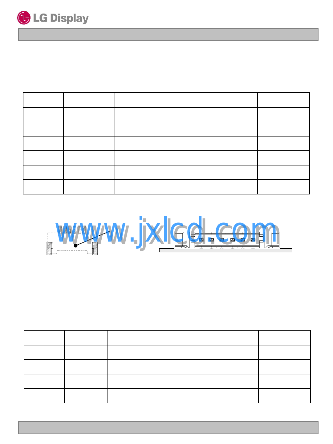
8-1. Designation of Lot Mark
a) Lot Mark
A B C D E F G H I J K L M
A,B,C : SIZE(INCH) D : YEAR
E : MONTH F ~ M : SERIAL NO.
Note
1. YEAR
LM215WF3
Liquid Crystal Display
Year
Mark
2. MONTH
Month
Mark
b) Location of Lot Mark
www.jxlcd.com
Serial No. is printed on the label. The label is attached to the backside of the LCD module.
This is subject to change without prior notice.
www.jxlcd.com
8-2. Packing Form
a) Package quantity in one box : 7pcs
b) Box Size : 360 * 310 * 562 (mm)
2006720078200892009
6
Jun7Jul8Aug9Sep
6
321
200452005
4
Apr5May
4
200320022001
2010
0
Oct
A
Nov
B
DecMarFebJan
C321
Ver. 1.0 January. 13 . 2011
29 / 35
Page 30

LM215WF3
Liquid Crystal Display
Product Specification
9. PRECAUTIONS
Please pay attention to the followings when you use this TFT LCD module.
9-1. MOUNTING PRECAUTIONS
(1) You must mount a module using holes arranged in four corners or four sides.
(2) You should consider the mounting structure so that uneven force (ex. Twisted stress) is not applied to the
module. And the case on which a module is mounted should have sufficient strength so that external
force is not transmitted directly to the module.
(3) Please attach the surface transparent protective plate to the surface in order to protect the polarizer.
Transparent protective plate should have sufficient strength in order to the resist external force.
(4) You should adopt radiation structure to satisfy the temperature specification.
(5) Acetic acid type and chlorine type materials for the cover case are not desirable because the former
generates corrosive gas of attacking the polarizer at high temperature and the latter causes circuit break
by electro-chemical reaction.
(6) Do not touch, push or rub the exposed polarizers with glass, tweezers or anything harder than HB
pencil lead. And please do not rub with dust clothes with chemical treatment.
Do not touch the surface of polarizer for bare hand or greasy cloth.(Some cosmetics are detrimental
to the polarizer.)
(7) When the surface becomes dusty, please wipe gently with absorbent cotton or other soft materials like
chamois soaks with petroleum benzene. Normal-hexane is recommended for cleaning the adhesives
used to attach front / rear polarizers. Do not use acetone, toluene and alcohol because they cause
chemical damage to the polarizer.
(8) Wipe off saliva or water drops as soon as possible. Their long time contact with polarizer causes
deformations and color fading.
(9) Do not open the case because inside circuits do not have sufficient strength.
www.jxlcd.com
www.jxlcd.com
9-2. OPERATING PRECAUTIONS
(1) The spike noise causes the mis-operation of circuits. It should be lower than following voltage :
V=±200mV(Over and under shoot voltage)
(2) Response time depends on the temperature.(In lower temperature, it becomes longer.)
(3) Brightness depends on the temperature. (In higher temperature, it becomes lower.)
And in lower temperature, response time(required time that brightness is stable after turned on) becomes
longer.
(4) Be careful for condensation at sudden temperature change. Condensation makes damage to polarizer or
electrical contacted parts. And after fading condensation, smear or spot will occur.
(5) When fixed patterns are displayed for a long time, remnant image is likely to occur.
(6) Module has high frequency circuits. Sufficient suppression to the electromagnetic interference shall be
done by system manufacturers. Grounding and shielding methods may be important to minimized the
interference.
(7) Please do not give any mechanical and/or acoustical impact to LCM. Otherwise, LCM can‟t be operated
its full characteristics perfectly.
(8) A screw which is fastened up the steels should be a machine screw.
(if not, it causes metallic foreign material and deal LCM a fatal blow)
(9) Please do not set LCD on its edge.
Ver. 1.0 January. 13 . 2011
30 / 35
Page 31

LM215WF3
Liquid Crystal Display
Product Specification
9-3. ELECTROSTATIC DISCHARGE CONTROL
Since a module is composed of electronic circuits, it is not strong to electrostatic discharge. Make certain that
treatment persons are connected to ground through wrist band etc. And don‟t touch interface pin directly.
9-4. PRECAUTIONS FOR STRONG LIGHT EXPOSURE
Strong light exposure causes degradation of polarizer and color filter.
9-5. STORAGE
When storing modules as spares for a long time, the following precautions are necessary.
(1) Store them in a dark place. Do not expose the module to sunlight or fluorescent light. Keep the temperature
between 5°C and 35°C at normal humidity.
(2) The polarizer surface should not come in contact with any other object.
It is recommended that they be stored in the container in which they were shipped.
9-6. HANDLING PRECAUTIONS FOR PROTECTION FILM
(1) The protection film is attached to the bezel with a small masking tape.
When the protection film is peeled off, static electricity is generated between the film and polarizer.
This should be peeled off slowly and carefully by people who are electrically grounded and with well ionblown equipment or in such a condition, etc.
(2) When the module with protection film attached is stored for a long time, sometimes there remains a very
small amount of glue still on the bezel after the protection film is peeled off.
(3) You can remove the glue easily. When the glue remains on the bezel surface or its vestige is recognized,
please wipe them off with absorbent cotton waste or other soft material like chamois soaked with normalhexane.
www.jxlcd.com
www.jxlcd.com
Ver. 1.0 January. 13 . 2011
31 / 35
Page 32

Product Specification
10. EDID DATA FOR LM215WF3-SDC2
10-1. EDID Data
LM215WF3-SDC2 EDID DATA (1920X1080 @ 60Hz )
LM215WF3
Liquid Crystal Display
www.jxlcd.com
www.jxlcd.com
Ver. 1.0 January. 13 . 2011
32 / 35
Page 33

Product Specification
LM215WF3
Liquid Crystal Display
www.jxlcd.com
www.jxlcd.com
Ver. 1.0 January. 13 . 2011
33 / 35
Page 34

Product Specification
LM215WF3
Liquid Crystal Display
www.jxlcd.com
www.jxlcd.com
Ver. 1.0 January. 13 . 2011
34 / 35
Page 35

Product Specification
LM215WF3
Liquid Crystal Display
www.jxlcd.com
www.jxlcd.com
10-2. EDID DATA READ/WRITE PROTOCOL
10-2-1. READ Operation
<Start><Slave Address, RW=0><Byte Address><Start><Slave Address, RW=1><Data><Stop>
10-2-2. WRITE Operation
<Start><Slave Address, RW=0><Byte Address><Data><Stop>
- Device Address (Slave Address)
Type Device (Slave) Address Hex
IS24C02B
- Byte Address
Decimal 0 ~ 255
Hex 0x00 ~ 0xFF
1 0 1 0 0 0 0
Byte Address
RW
0xA0 + RW
Ver. 1.0 January. 13 . 2011
35 / 35
 Loading...