

Page 1
Order this document by LM311/D
The ability to operate from a single power supply of 5.0 V to 30 V or ±15 V
split supplies, as commonly used with operational amplifiers, makes the
LM211/LM311 a truly versatile comparator. Moreover, the inputs of the
device can be isolated from system ground while the output can drive loads
referenced either to ground, the VCC or the VEE supply . This flexibility makes
it possible to drive DTL, RTL, TTL, or MOS logic. The output can also switch
voltages to 50 V at currents to 50 mA. Thus the LM21 1/LM31 1 can be used to
drive relays, lamps or solenoids.
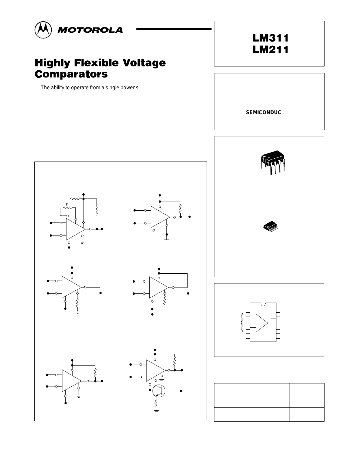
T ypical Comparator Design Configurations
Split Power Supply with Offset Balance
V
EE
V
8
1
V
8
6
CC
CC
CC
R
L
8
7
Output
1
7
Output
R
L
R
L
7
1
Output
Inputs
Load Referred to Negative Supply
Inputs
Inputs
3.0 k
5.0 k
5
2
+
Inputs
3
–
4
V
Ground–Referred Load
2
+
Inputs
3
–
4
V
EE
Input polarity is reversed when
Gnd pin is used as an output.
Load Referred to Positive Supply Strobe Capability
2
+
Inputs
3
–
4
V
EE
Single Supply
V
CC
2
3
V
2
3
Input polarity is reversed when
Gnd pin is used as an output.
V
2
3
4
V
EE
EE
CC
+
–
8
+
–
4
V
CC
8
+
–
1
4
V
EE
8
1
6
1.0 k
1
R
L
7
7
7
R
L
R
L
Output
Output
Output
TTL Strobe
HIGH PERFORMANCE
VOLTAGE COMPARATORS
SEMICONDUCTOR
TECHNICAL DATA
8
1
N SUFFIX
PLASTIC PACKAGE
CASE 626
8
1
D SUFFIX
PLASTIC PACKAGE
CASE 751
(SO–8)
PIN CONNECTIONS
V
8
CC
7
Output
6
Balance/Strobe
5
Balance
Inputs
Device
LM211D
LM311D
LM311N
Gnd
1
2
+
3
–
4
V
EE
(Top View)
ORDERING INFORMATION
Operating
Temperature Range
TA = 25° to +85°C
TA = 0° to +70°C
Package
SO–8
SO–8
Plastic DIP
MOTOROLA ANALOG IC DEVICE DATA
Motorola, Inc. 1996 Rev 5
1
Page 2
LM311 LM211
MAXIMUM RATINGS (T
= +25°C, unless otherwise noted.)
A
Rating Symbol LM211 LM311 Unit
Total Supply Voltage VCC +VEE 36 36 Vdc
Output to Negative Supply Voltage VO –V
Ground to Negative Supply Voltage V
EE
Input Differential Voltage V
Input Voltage (Note 2) V
EE
ID
in
50 40 Vdc
30 30 Vdc
±30 ±30 Vdc
±15 ±15 Vdc
Voltage at Strobe Pin – VCC to VCC–5 VCC to VCC–5 Vdc
Power Dissipation and Thermal Characteristics
Plastic DIP P
Derate Above TA = +25°C 1/θ
Operating Ambient Temperature Range T
Operating Junction Temperature T
Storage Temperature Range T
ELECTRICAL CHARACTERISTICS (V
= +15 V, VEE = –15 V, TA = 25°C, unless otherwise noted [Note 1].)
CC
D
JA
A
J(max)
stg
–25 to +85 0 to +70 °C
+150 +150 °C
–65 to +150 –65 to +150 °C
625 mW
5.0 mW/°C
LM211 LM311
Characteristic Symbol
Input Offset Voltage (Note 3) V
IO
Min Typ Max Min Typ Max
RS ≤ 50 kΩ, TA = +25°C – 0.7 3.0 – 2.0 7.5
RS ≤ 50 kΩ, T
Input Offset Current (Note 3) TA = +25°C I
T
≤ TA ≤ T
low
Input Bias Current TA = +25°C I
T
≤ TA ≤ T
low
Voltage Gain A
≤ TA ≤ T
low
* – – 20 – – 70
high
* – – 150 – – 300
high
* – – 4.0 – – 10
high
IO
IB
V
– 1.7 10 – 1.7 50 nA
– 45 100 – 45 250 nA
40 200 – 40 200 – V/mV
Response Time (Note 4) – 200 – – 200 – ns
Saturation Voltage V
OL
VID ≤ –5.0 mV, IO = 50 mA, TA = 25°C – 0.75 1.5 – – –
VID ≤–10 mV , IO = 50 mA, TA = 25°C – – – – 0.75 1.5
VCC ≥ 4.5 V, VEE = 0, T
VID 6≤6.0 mV , I
VID 6≤10 mV , I
sink
sink
Strobe ”On” Current (Note 5) I
≤ TA ≤ T
low
≤ 8.0 mA
≤ 8.0 mA
high
*
– 0.23 0.4 – – –
– – – – 0.23 0.4
S
– 3.0 – – 3.0 – mA
Output Leakage Current
VID ≥ 5.0 mV, VO= 35 V, TA = 25°C, I
VID
≥ 10 mV , VO
VID
≥ 5.0 mV , VO
Input Voltage Range (T
= 35 V, TA = 25°C, I
= 35 V, T
low
≤ TA ≤ T
low
≤ TA ≤ T
high
Positive Supply Current I
Negative Supply Current I
* T
= –25°C for LM211 T
low
= 0°C for LM311 = +70°C for LM311
NOTES: 1. Of fset voltage, of fset current and bias current specifications apply for a supply voltage range from a single 5.0 V supply up to ±15V supplies.
2.This rating applies for ±15 V supplies. The positive input voltage limit is 30 V above the negative supply. The negative input voltage limit is equal to the
negative supply voltage or 30 V below the positive supply , whichever is less.
3.The offset voltages and offset currents given are the maximum values required to drive the output within a volt of either supply with a 1.0 mA load. Thus,
these parameters define an error band and take into account the ”worst case” effects of voltage gain and input impedance.
4.The response time specified is for a 100 mV input step with 5.0 mV overdrive.
5.Do not short the strobe pin to ground; it should be current driven at 3.0 mA to 5.0 mA.
= 3.0 mA – 0.2 10 – – – nA
strobe
= 3.0 mA – – – – 0.2 50 nA
strobe
* – 0.1 0.5 – – – µA
high
*) V
high
ICR
CC
EE
= +85°C for LM211
–14.5 –14.7 to
13.8
+13.0 –14.5 –14.7 to
13.8
– +2.4 +6.0 – +2.4 +7.5 mA
– –1.3 –5.0 – –1.3 –5.0 mA
+13.0 V
Unit
mV
V
2
MOTOROLA ANALOG IC DEVICE DATA
Page 3
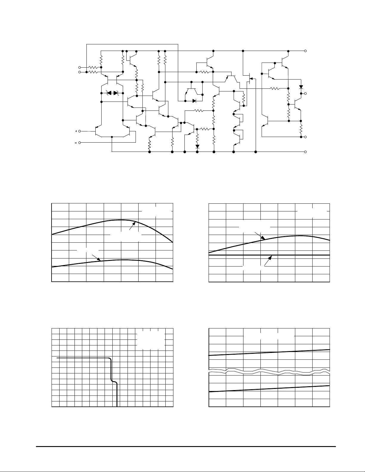
Balance
Balance/Strobe
Inputs
LM311 LM211
Figure 1. Circuit Schematic
8
V
7
Output
1
Gnd
4
V
CC
EE
1.3 k
3005
300
6
2
3
1.3 k
3.7 k
100
3.7 k
730
340
800800
3.0 k
5.0 k
200
600
250
1.3 k
1.3 k
300
900
800
5.4 k
Figure 2. Input Bias Current
versus T emperature
140
120
100
80
, INPUT BIAS CURRENT (nA)
IB
40
I
0
–55 –25 0 25 50 75 100 125
Normal
TA, TEMPERATURE (°C) TA, TEMPERATURE (°C)
Pins 5 & 6 Tied
to V
VCC = +15 V
VEE = –15 V
CC
Figure 4. Input Bias Current versus
Differential Input Voltage
140
120
100
80
VCC = +15 V
VEE = –15 V
°
TA = +25
Figure 3. Input Offset Current
versus T emperature
5.0
VCC = +15 V
4.0
3.0
2.0
1.0
, INPUT OFFSET CURRENT (nA)COMMON MODE LIMITS (V)
IO
I
0
–55 –25 0 25 50 75 100 125
Pins 5 & 6 Tied
to V
CC
Normal
VEE = –15 V
Figure 5. Common Mode Limits
versus T emperature
V
CC
C
–0.5
–1.0
–1.5
Referred to Supply Voltages
60
40
, INPUT BIAS CURRENT (nA)
IB
I
20
0
–16 –12 –8.0 –4.0 0 4.0 8.0 12 16
DIFFERENTIAL INPUT VOLTAGE (V)
MOTOROLA ANALOG IC DEVICE DATA
0.4
0.2
V
EE
–55 –25 0 25 50 75 100 125
TA, TEMPERATURE (°C)
3
Page 4

LM311 LM211
5.0
4.0
20 mV
3.0
, OUTPUT VOL TAGE (V)
O
2.0
V
1.0
0
100
50
0
INPUT VOLTAGE (mV)
,
V
0 0.1 0.2 0.3 0.4 0.5 0.6
in
15
10
20 mV 5.0 mV
5.0
0
, OUTPUT VOL TAGE (V)
–5.0
O
V
–10
–15
0
–50
–100
INPUT VOLTAGE (mV)
,
V
0 1.0 2.0
in
Figure 6. Response Time for
Various Input Overdrives
5.0 mV
V
*
in
)
2.0 mV
VCC = +15 V
VEE = –15 V
TA = +25
t
, RESPONSE TIME (µs) t
TLH
Figure 8. Response Time for
Various Input Overdrives
V
2.0 mV
µ
t
, RESPONSE TIME (
TLH
s) t
+5.0 V
500
Ω
V
O
°
C
V
CC
in
*
)
2.0 k
V
EE
VCC = +15 V
VEE = –15 V
°
C
TA = +25
Figure 7. Response Time for
Various Input Overdrives
+5.0 V
Ω
500
V
O
, OUTPUT VOL TAGE (V)
V
5.0
4.0
3.0
2.0
1.0
20 mV
O
5.0 mV
2.0 mV
V
in
*
)
0
0
–50
VCC = +15 V
VEE = –15 V
°
TA = +25
C
–100
INPUT VOLTAGE (mV)
,
in
V
0 0.1 0.2 0.3 0.4 0.5 0.6
, RESPONSE TIME (µs)
THL
Figure 9. Response Time for
Various Input Overdrives
V
15
10
5.0
0
V
O
, OUTPUT VOL TAGE (V)
V
O
–5.0
–10
–15
20 mV
5.0 mV
2.0 mV
100
50
0
INPUT VOLTAGE (mV)
,
in
V
0 1.0 2.0
, RESPONSE TIME (µs)
THL
CC
V
in
*
)
V
EE
VCC = +15 V
VEE = –15 V
°
C
TA = +25
2.0 k
V
O
Figure 10. Output Short Circuit Current
Characteristics and Power Dissipation
150
125
100
Power Dissipation
75
50
25
OUTPUT SHORT CIRCUIT CURRENT (mA)
0
0 5.0 10 15
VO, OUTPUT VOLTAGE (V) IO, OUTPUT CURRENT (mA)
TA = +25°C
Short Circuit Current
4
0.90
0.75
0.60
0.45
0.30
0.15
0
, SATURATION VOLTAGE (V)
, POWER DISSIPATION (W)
D
OL
P
V
Figure 11. Output Saturation Voltage
versus Output Current
0.90
0.75
0.60
TA = –55°C
0.45
0.30
TA = +25°C
0.15
TA = +125°C
0
0 8.0 16 24 32 40 48 56
MOTOROLA ANALOG IC DEVICE DATA
Page 5

LM311 LM211
Figure 12. Output Leakage Current
versus T emperature
100
VCC = +15 V
10
1.0
0.1
OUTPUT LEAKAGE CURRENT (mA)
0.01
VEE = –15 V
Output VO = +50 V (LM11/211 only)
25 45 65 85 105 125
TA, TEMPERATURE (°C)
Figure 14. Power Supply Current
3.0
2.6
Postive Supply – Output Low
2.2
3.6
3.0
2.4
1.8
1.2
0.6
POWER SUPPLY CURRENT (mA)
0
0 5.0 10 15 20 25 30
versus T emperature
Figure 13. Power Supply Current
versus Supply V oltage
TA = +25°C
Positive Supply – Output Low
Positive and Negative Power Supply – Output H igh
VCC–VEE, POWER SUPPLY VOLTAGE (V)
VCC = +15 V
VEE = –15 V
1.8
SUPPLY CURRENT (mA)
1.4
1.0
–55 –25 0 25 50 75 100 125
Figure 15. Improved Method of Adding
Hysteresis Without Applying Positive
Feedback to the Inputs
33 k
8
+
LM311
–
6
5.0 k
C1
0.002
µ
F
5
7
1
Input
0.1
R1
µ
F
2
C2
R2
34
Positive and Negative Supply – Output High
TA, TEMPERATURE (
°
C)
APPLICATIONS INFORMATION
Figure 16. Conventional T echnique
+15 V
823.0 k
0.1
4.7 k
100
Input
R1
Output
100
R2
for Adding Hysteresis
8
+
LM311
–
6
5.0 k
C1
C2
µ
F
3
24
3.0 k
1
5
7
+15 V
4.7 k
Output
0.1 µF
–15 V
MOTOROLA ANALOG IC DEVICE DATA
1.0 M
–15 V
0.1 µF
510 k
5
Page 6

LM311 LM211
TECHNIQUES FOR AVOIDING OSCILLATIONS IN COMPARATOR APPLICATIONS
When a high speed comparator such as the LM21 1 is used
with high speed input signals and low source impedances,
the output response will normally be fast and stable,
providing the power supplies have been bypassed (with 0.1 µF
disc capacitors), and that the output signal is routed well
away from the inputs (Pins 2 and 3) and also away from Pins
5 and 6.
However, when the input signal is a voltage ramp or a slow
sine wave, or if the signal source impedance is high (1.0 kΩ
to 100 kΩ), the comparator may burst into oscillation near the
crossing–point. This is due to the high gain and wide
bandwidth of comparators like the LM211 series. To avoid
oscillation or instability in such a usage, several precautions
are recommended, as shown in Figure 15.
The trim pins (Pins 5 and 6) act as unwanted auxiliary
inputs. If these pins are not connected to a trim–pot, they
should be shorted together. If they are connected to a
trim–pot, a 0.01 µF capacitor (C1) between Pins 5 and 6 will
minimize the susceptibility to AC coupling. A smaller
capacitor is used if Pin 5 is used for positive feedback as in
Figure 15. For the fastest response time, tie both balance
pins to VCC.
Certain sources will produce a cleaner comparator output
waveform if a 100 pF to 1000 pF capacitor (C2) is connected
directly across the input pins. When the signal source is
applied through a resistive network, R1, it is usually
advantageous to choose R2 of the same value, both for DC
and for dynamic (AC) considerations. Carbon, tin–oxide, and
metal–film resistors have all been used with good results in
comparator input circuitry, but inductive wirewound resistors
should be avoided.
When comparator circuits use input resistors (e.g.,
summing resistors), their value and placement are
particularly important. In all cases the body of the resistor
should be close to the device or socket. In other words, there
should be a very short lead length or printed–circuit foil run
between comparator and resistor to radiate or pick up
signals. The same applies to capacitors, pots, etc. For
example, if R1 = 10 kΩ, as little as 5 inches of lead between
the resistors and the input pins can result in oscillations that
are very hard to dampen. Twisting these input leads tightly is
the best alternative to placing resistors close to the
comparator.
Since feedback to almost any pin of a comparator can
result in oscillation, the printed–circuit layout should be
engineered thoughtfully. Preferably there should be a
groundplane under the LM211 circuitry (e.g., one side of a
double layer printed circuit board). Ground, positive supply or
negative supply foil should extend between the output and
the inputs to act as a guard. The foil connections for the
inputs should be as small and compact as possible, and
should be essentially surrounded by ground foil on all sides to
guard against capacitive coupling from any fast high–level
signals (such as the output). If Pins 5 and 6 are not used, they
should be shorted together. If they are connected to a
trim–pot, the trim–pot should be located no more than a few
inches away from the LM21 1, and a 0.01 µF capacitor should
be installed across Pins 5 and 6. If this capacitor cannot be
used, a shielding printed–circuit foil may be advisable
between Pins 6 and 7. The power supply bypass capacitors
should be located within a couple inches of the LM21 1.
A standard procedure is to add hysteresis to a comparator
to prevent oscillation, and to avoid excessive noise on the
output. In the circuit of Figure 16, the feedback resistor of
510 kΩ from the output to the positive input will cause about
3.0 mV of hysteresis. However, if R2 is larger than 100 Ω,
such as 50 kΩ, it would not be practical to simply increase the
value of the positive feedback resistor proportionally above
510 kΩ to maintain the same amount of hysteresis.
When both inputs of the LM211 are connected to active
signals, or if a high–impedance signal is driving the positive
input of the LM211 so that positive feedback would be
disruptive, the circuit of Figure 15 is ideal. The positive
feedback is applied to Pin 5 (one of the offset adjustment
pins). This will be sufficient to cause 1.0 mV to 2.0 mV
hysteresis and sharp transitions with input triangle waves
from a few Hz to hundreds of kHz. The positive–feedback
signal across the 82 Ω resistor swings 240 mV below the
positive supply. This signal is centered around the nominal
voltage at Pin 5, so this feedback does not add to the offset
voltage of the comparator. As much as 8.0 mV of offset
voltage can be trimmed out, using the 5.0 kΩ pot and 3.0 kΩ
resistor as shown.
6
Figure 17. Zero–Crossing Detector
Driving CMOS Logic
VCC = +15 V
Balance
Adjust
Balance
Input
Inputs
3.0 k
5.0 k
+
LM311
V
EE
VEE = –15 V
V
Gnd
CC
10 k
Output
to CMOS Logic
Figure 18. Relay Driver with Strobe Capability
2N2222
or Equiv
V
CC2
*D1
*Zener Diode D1
protects the comparator
from inductive kickback
and voltage transients
on the V
CC2
supply line.
Inputs
V
EE
V
EE
Gnd
+
LM311
V
CC1
V
CC
Output
Balance/Strobe
Q1
1.0 k
TTL
Strobe
MOTOROLA ANALOG IC DEVICE DATA
Page 7

NOTE 2
–T–
SEATING
PLANE
H
OUTLINE DIMENSIONS
58
–B–
14
F
–A–
C
N
D
G
0.13 (0.005) B
K
M
T
LM311 LM211
N SUFFIX
PLASTIC PACKAGE
CASE 626–05
ISSUE K
L
J
M
M
A
M
NOTES:
1. DIMENSION L TO CENTER OF LEAD WHEN
FORMED PARALLEL.
2. PACKAGE CONTOUR OPTIONAL (ROUND OR
SQUARE CORNERS).
3. DIMENSIONING AND TOLERANCING PER ANSI
Y14.5M, 1982.
DIM MIN MAX MIN MAX
A 9.40 10.16 0.370 0.400
B 6.10 6.60 0.240 0.260
C 3.94 4.45 0.155 0.175
D 0.38 0.51 0.015 0.020
F 1.02 1.78 0.040 0.070
G 2.54 BSC 0.100 BSC
H 0.76 1.27 0.030 0.050
J 0.20 0.30 0.008 0.012
K 2.92 3.43 0.115 0.135
L 7.62 BSC 0.300 BSC
M ––– 10 ––– 10
N 0.76 1.01 0.030 0.040
INCHESMILLIMETERS
__
A
C
E
B
A1
D SUFFIX
PLASTIC PACKAGE
CASE 751–05
(SO–8)
ISSUE R
D
58
0.25MB
1
H
4
e
M
h
X 45
_
q
C
A
SEATING
PLANE
0.10
L
B
SS
A0.25MCB
NOTES:
1. DIMENSIONING AND TOLERANCING PER ASME
Y14.5M, 1994.
2. DIMENSIONS ARE IN MILLIMETERS.
3. DIMENSION D AND E DO NOT INCLUDE MOLD
PROTRUSION.
4. MAXIMUM MOLD PROTRUSION 0.15 PER SIDE.
5. DIMENSION B DOES NOT INCLUDE MOLD
PROTRUSION. ALLOWABLE DAMBAR
PROTRUSION SHALL BE 0.127 TOTAL IN EXCESS
OF THE B DIMENSION AT MAXIMUM MATERIAL
CONDITION.
MILLIMETERS
DIM MIN MAX
A 1.35 1.75
A1 0.10 0.25
B 0.35 0.49
C 0.18 0.25
D 4.80 5.00
E
3.80 4.00
1.27 BSCe
H 5.80 6.20
h
0.25 0.50
L 0.40 1.25
0 7
q
__
MOTOROLA ANALOG IC DEVICE DATA
7
Page 8

LM311 LM211
Motorola reserves the right to make changes without further notice to any products herein. Motorola makes no warranty , representation or guarantee regarding
the suitability of its products for any particular purpose, nor does Motorola assume any liability arising out of the application or use of any product or circuit, and
specifically disclaims any and all liability, including without limitation consequential or incidental damages. “T ypical” parameters which may be provided in Motorola
data sheets and/or specifications can and do vary in different applications and actual performance may vary over time. All operating parameters, including “Typicals”
must be validated for each customer application by customer’s technical experts. Motorola does not convey any license under its patent rights nor the rights of
others. Motorola products are not designed, intended, or authorized for use as components in systems intended for surgical implant into the body, or other
applications intended to support or sustain life, or for any other application in which the failure of the Motorola product could create a situation where personal injury
or death may occur. Should Buyer purchase or use Motorola products for any such unintended or unauthorized application, Buyer shall indemnify and hold Motorola
and its officers, employees, subsidiaries, affiliates, and distributors harmless against all claims, costs, damages, and expenses, and reasonable attorney fees
arising out of, directly or indirectly, any claim of personal injury or death associated with such unintended or unauthorized use, even if such claim alleges that
Motorola was negligent regarding the design or manufacture of the part. Motorola and are registered trademarks of Motorola, Inc. Motorola, Inc. is an Equal
Opportunity/Affirmative Action Employer.
How to reach us:
USA/EUROPE/Locations Not Listed: Motorola Literature Distribution; JAPAN: Nippon Motorola Ltd.; Tatsumi–SPD–JLDC, 6F Seibu–Butsuryu–Center,
P.O. Box 20912; Phoenix, Arizona 85036. 1–800–441–2447 or 602–303–5454 3–14–2 Tatsumi Koto–Ku, Tokyo 135, Japan. 03–81–3521–8315
MFAX: RMF AX0@email.sps.mot.com – TOUCHT ONE 602–244–6609 ASIA/PACIFIC: Motorola Semiconductors H.K. Ltd.; 8B Tai Ping Industrial Park,
INTERNET: http://Design–NET.com 51 Ting Kok Road, Tai Po, N.T., Hong Kong. 852–26629298
8
◊
MOTOROLA ANALOG IC DEVICE DATA
LM311/D
*LM311/D*
 Loading...