

Page 1
LM20
2.4V, 10µA, SC70, micro SMD Temperature Sensor
General Description
The LM20 is a precision analog output CMOS
integrated-circuit temperature sensor that operates over a
−55˚C to +130˚C temperature range. The power supply operating range is +2.4 V to +5.5 V. The transfer function of
LM20 is predominately linear, yet has a slight predictable
parabolic curvature. The accuracy of the LM20 when specified to a parabolic transfer function is
temperature of +30˚C. The temperature error increases linearly and reaches a maximum of
range extremes. The temperature range is affected by the
power supply voltage. At a power supply voltage of 2.7 V to
5.5 V the temperature range extremes are +130˚C and
−55˚C. Decreasing the power supply voltage to 2.4 V
changes the negative extreme to −30˚C, while the positive
remains at +130˚C.
The LM20’s quiescent current is less than 10 µA. Therefore,
self-heating is less than 0.02˚C in stillair. Shutdown capability for the LM20 is intrinsic because its inherent low power
consumption allows it to be powered directly from the output
of many logic gates or does not necessitate shutdown at all.
±
1.5˚C at an ambient
±
2.5˚C at the temperature
Applications
n Cellular Phones
n Computers
n Power Supply Modules
n Battery Management
n FAX Machines
n Printers
n HVAC
n Disk Drives
n Appliances
Features
n Rated for full −55˚C to +130˚C range
n Available in an SC70 and a micro SMD package
n Predictable curvature error
n Suitable for remote applications
Key Specifications
n Accuracy at +30˚C
n Accuracy at +130˚C & −55˚C
n Power Supply Voltage Range +2.4V to +5.5V
n Current Drain 10 µA (max)
n Nonlinearity
n Output Impedance 160 Ω (max)
n Load Regulation
0µA
<
<
I
+16 µA −2.5 mV (max)
L
±
1.5 to±4 ˚C (max)
±
2.5 to±5 ˚C (max)
October 1999
±
0.4%(typ)
LM20 2.4V, 10µA, SC70, micro SMD Temperature Sensor
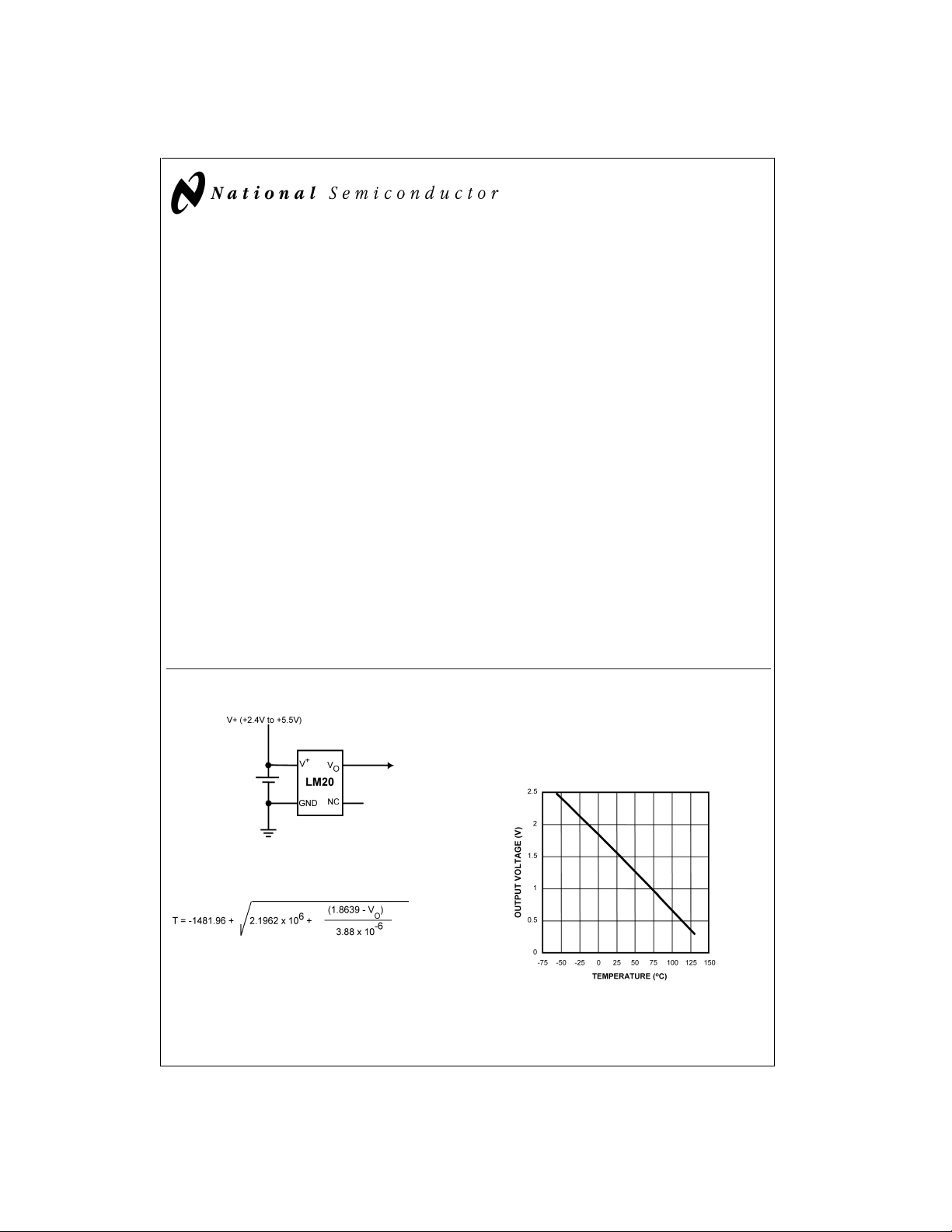
Typical Application
Output Voltage vs Temperature
DS100908-2
=
V
(−3.88x10
O
or
where:
T is temperature, and V
© 1999 National Semiconductor Corporation DS100908 www.national.com
−6xT2
) + (−1.15x10⁻²xT) + 1.8639
is the measured output voltage of the LM20.
O
Full-Range Celsius (Centigrade) Temperature Sensor (−55˚C to +130˚C)
Operating from a Single Li-Ion Battery Cell
DS100908-24
Page 2
Typical Application (Continued)
LM20
Temperature (T) Typical V
+130˚C +303 mV
+100˚C +675 mV
+80˚C +919 mV
+30˚C +1515 mV
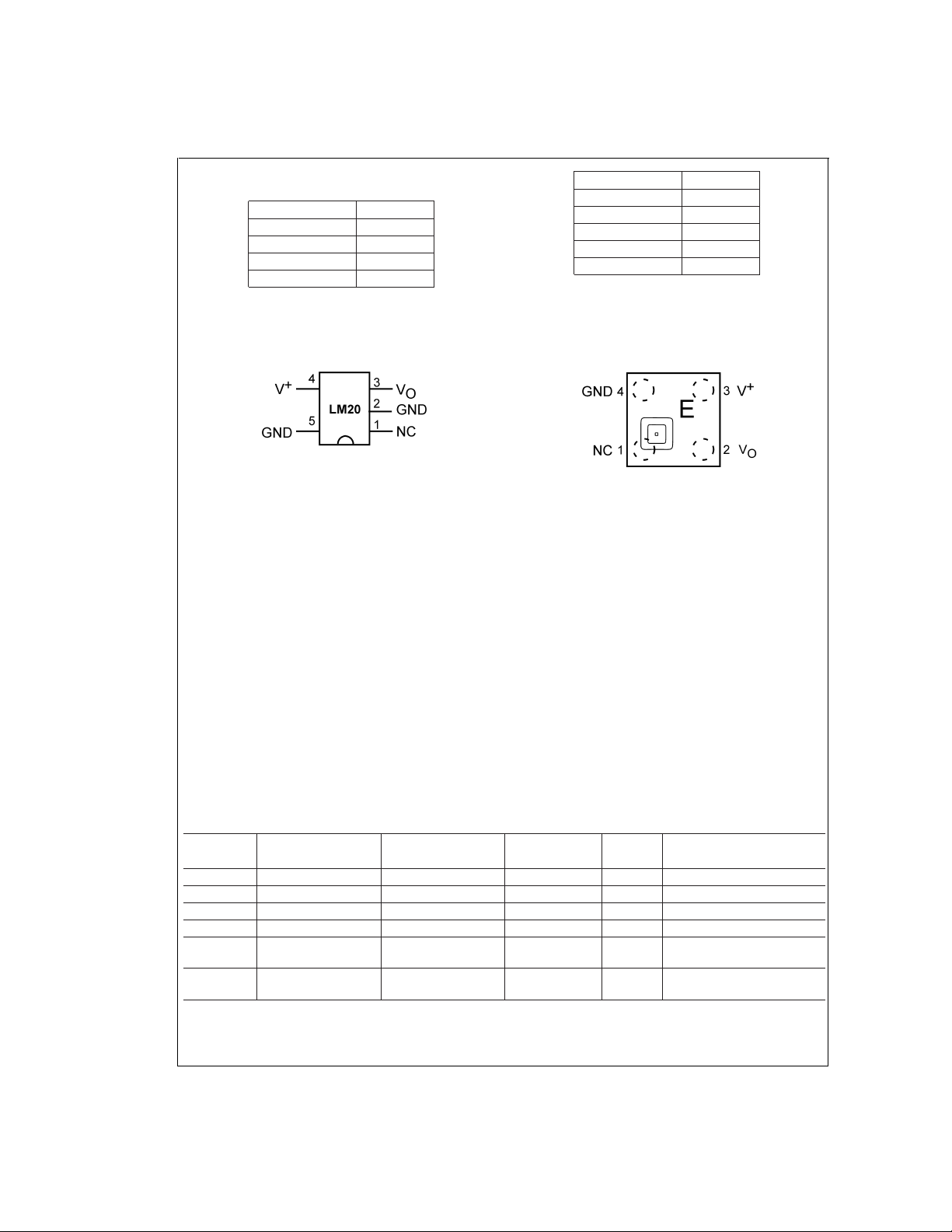
Connection Diagrams
Temperature (T) Typical V
O
+25˚C +1574 mV
O
0˚C +1863.9 mV
−30˚C +2205 mV
−40˚C +2318 mV
−55˚C +2485 mV
SC70-5
Note:
- GND (pin 2) may be grounded or left floating. For optimum thermal
conductivity to the pc board ground plane pin 2 should be grounded.
- NC (pin 1) should be left floating or grounded. Other signal traces
should not be connected to this pin.
DS100908-1
Top View
See NS Package Number MAA05A
micro SMD
Note:
- Pin numbers are referenced to the package marking text orientation.
- Reference JEDEC Registration MO-211, variation BA
- The actual physical placement of package marking will vary slightly
from part to part. The package marking will designate the date code and
will vary considerably. Package marking does not correlate to device type
in any way.
DS100908-32
Top View
See NS Package Number BPA04DDC
Ordering Information
Order Temperature Temperature NS Package Device
Number Accuracy Range Number Marking Transport Media
LM20BIM7
LM20BIM7X
LM20CIM7
LM20CIM7X
LM20SIBP
LM20SIBPX
www.national.com 2
±
2.5˚C −55˚C to +130˚C MAA05A T2B 1000 Units on Tape and Reel
±
2.5˚C −55˚C to +130˚C MAA05A T2B 3000 Units on Tape and Reel
±
5˚C −55˚C to +130˚C MAA05A T2C 1000 Units on Tape and Reel
±
5˚C −55˚C to +130˚C MAA05A T2C 3000 Units on Tape and Reel
±
3.5˚C −40˚C to +125˚C BPA04DDC Date
250 Units on Tape and Reel
Code
±
3.5˚C −40˚C to +125˚C BPA04DDC Date
3000 Units on Tape and Reel
Code
Page 3
Absolute Maximum Ratings (Note 1)
Supply Voltage +6.5V to −0.2V
Output Voltage (V
Output Current 10 mA
Input Current at any pin (Note 2) 5 mA
Storage Temperature −65˚C to +150˚C
Maximum Junction Temperature (T
JMAX
ESD Susceptibility (Note 3) :
Human Body Model 2500 V
Machine Model 250 V
Electrical Characteristics
Unless otherwise noted, these specifications apply for V
other limits T
=
=
T
25˚C; Unless otherwise noted.
A
J
Parameter Conditions Typical
+
+ 0.6 V) to
−0.6 V
) +150˚C
+
=
Lead Temperature
SC-70 Package (Note 4) :
Vapor Phase (60 seconds) +215˚C
Infrared (15 seconds) +220˚C
Operating Ratings(Note 1)
Specified Temperature Range: T
LM20B, LM20C with
LM20B, LM20C with
LM20S with
LM20S with
Supply Voltage Range (V
Thermal Resistance, θ
SC-70
micro SMD
. Boldface limits apply for T
+2.7 V
DC
(Note 6)
+
2.4 V ≤ V
2.7 V ≤ V
2.4 V ≤ V
2.7 V ≤ V
≤ 2.7 V −30˚C ≤ TA≤ +130˚C
+
≤ 5.5 V −55˚C ≤ TA≤ +130˚C
+
≤ 5.5 V −30˚C ≤ TA≤ +125˚C
+
≤ 5.5 V −40˚C ≤ TA≤ +125˚C
+
(Note 5)
JA
LM20B LM20C LM20S Units
Limits Limits Limits
≤ TA≤ T
MIN
) +2.4 V to +5.5 V
415˚C/W
TBD˚C/W
=
=
T
A
to T
T
J
MIN
MAX
(Limit)
(Note 7) (Note 7) (Note 7)
Temperature to Voltage Error
=
(−3.88x10
V
O
+ (−1.15x10
−6xT2
)
−2
xT) + 1.8639V
(Note 8)
= +25˚C to +30˚C
T
A
T
= +130˚C
A
T
= +125˚C
A
T
= +100˚C
A
T
= +85˚C
A
T
= +80˚C
A
T
= 0˚C
A
T
= −30˚C
A
T
= −40˚C
A
T
= −55˚C
A
±
1.5
±
2.5
±
2.5
±
2.2
±
2.1
±
2.0
±
1.9
±
2.2
±
2.3
±
2.5
±
4.0
±
5.0 ˚C (max)
±
5.0
±
4.7
±
4.6
±
4.5
±
4.4
±
4.7
±
4.8
±
5.0 ˚C (max)
±
2.5 ˚C (max)
±
3.5 ˚C (max)
±
3.2 ˚C (max)
±
3.1 ˚C (max)
±
3.0 ˚C (max)
±
2.9 ˚C (max)
±
3.3 ˚C (min)
±
3.5 ˚C (max)
Output Voltage at 0˚C +1.8639 V
Variance from Curve
Non-Linearity (Note 9) −20˚C ≤ T
Sensor Gain (Temperature
−30˚C ≤ T
Sensitivity or Average Slope)
≤ +80˚C
A
≤ +100˚C −11.77 −11.4
A
±
1.0 ˚C
±
0.4
−12.2
−11.0
−12.6
−11.0
−12.6
mV/˚C (min)
mV/˚C (max)
%
to equation:
=
−11.77 mV/˚CxT+1.860V
V
O
Output Impedance 0 µA ≤ I
11, 12)
Load Regulation(Note 10) 0 µA ≤ I
11, 12)
Line Regulation +2. 4 V ≤ V
+5.0 V ≤ V
Quiescent Current +2. 4 V ≤ V
+2.4V≤V
Change of Quiescent Current +2. 4 V ≤ V
≤ +16 µA(Notes
L
≤ +16 µA(Notes
L
+
≤ +5.0V +3.3 +3.7 +3.7 mV/V (max)
+
≤ +5.5 V +8.8 +8.9 +8.9 mV (max)
+
≤ +5.5V 4.5 7 7 7 µA (max)
+
≤+5.0V 4.5 10 10 10 µA (max)
+
≤ +5.5V +0.7 µA
160 160 160 Ω (max)
−2.5 −2.5 −2.5 mV (max)
Temperature Coefficient of −11 nA/˚C
Quiescent Current
Shutdown Current V
+
≤ +0.8 V 0.02 µA
LM20
MAX
; all
www.national.com3
Page 4

Electrical Characteristics (Continued)
LM20
Note 1: Absolute Maximum Ratings indicate limits beyond which damage to the device may occur. Operating Ratings indicate conditions for which the device is func-
tional, but do not guarantee specific performance limits. For guaranteed specifications and test conditions, see the Electrical Characteristics. The guaranteed specifications apply only for the test conditions listed. Some performance characteristics may degrade when the device is not operated under the listed test conditions.
Note 2: When the input voltage (V
Note 3: The human body model is a 100 pF capacitor discharged through a 1.5 kΩ resistor into each pin. The machine model is a 200 pF capacitor discharged di-
rectly into each pin.
Note 4: See AN-450 “Surface Mounting Methods and Their Effect on Product Reliability” or the section titled “Surface Mount” found in any post 1986 National Semi-
conductor Linear Data Book for other methods of soldering surface mount devices.
Note 5: The junction to ambient thermal resistance (θ
FOR fig NS1382*
Note 6: Typicals are at T
Note 7: Limits are guaranteed to National’s AOQL (Average Outgoing Quality Level).
Note 8: Accuracy is defined as the error between the measured and calculated output voltage at the specified conditions of voltage, current, and temperature (ex-
pressed in˚C).
Note 9: Non-Linearity is defined as the deviation of the calculated output-voltage-versus-temperature curve from the best-fit straight line, over the temperature range
specified.
Note 10: Regulation is measured at constant junction temperature, using pulse testing with a low duty cycle. Changes in output due to heating effects can be com-
puted by multiplying the internal dissipation by the thermal resistance.
Note 11: Negative currents are flowing into the LM20. Positive currents are flowing out of the LM20. Using this convention the LM20 can at most sink −1 µA and
source +16 µA.
Note 12: Load regulation or output impedance specifications apply over the supply voltage range of +2.4V to +5.5V.
Note 13: Line regulation is calculated by subtracting the output voltage at the highest supply input voltage from the output voltage at the lowest supply input voltage.
.
) at any pin exceeds power supplies (V
I
) is specified without a heat sink in still air using the printed circuit board layout shown in
JA
=
=
T
25˚C and represent most likely parametric norm.
J
A
<
I
GND or V
>
V+), the current at that pin should be limited to 5 mA.
I
Figure *NO TARGET
Typical Performance Characteristics
Temperature Error vs Temperature
DS100908-25
PCB Layouts Used for Thermal
Measurements
DS100908-29
a) Layout used for no heat sink measurements.
FIGURE 1. PCB Lyouts used for thermal measurements.
www.national.com 4
DS100908-30
b) Layout used for measurements with small heat hink.
Page 5

1.0 LM20 Transfer Function
The LM20’s transfer function can be described in different
ways with varying levels of precision.A simple linear transfer
function, with good accuracy near 25˚C, is
Over the full operating temperature range of −55˚C to
+130˚C, best accuracy can be obtained by using the parabolic transfer function
V
solving for T:
Alinear transfer function can be used over a limited temperature range by calculating a slope and offset that give best results over that range. A linear transfer function can be calculated from the parabolic transfer function of the LM20. The
slope of the linear transfer function can be calculated using
the following equation:
=
O
(−3.88x10
=
V
−11.69 mV/˚C x T + 1.8663 V
O
−6xT2
) + (−1.15x10⁻²xT) + 1.8639
m=−7.76 x 10
−6
x T − 0.0115,
where T is the middle of the temperature range of interest
and m is in V/˚C. For example for the temperature range of
T
min
=
−30 to T
max
=
+100˚C:
T=35˚C
and
m = −11.77 mV/˚C
The offset of the linear transfer function can be calculated
using the following equation:
b=(V
)+VOP(T)+mx(T
OP(Tmax
max
+T))/2,
where:
VOP(T
•
•
) is the calculated output voltage at T
max
the parabolic transfer function for V
O
VOP(T) is the calculated output voltage at T using the
parabolic transfer function for V
.
O
max
using
Using this procedure the best fit linear transfer function for
many popular temperature ranges was calculated in
2
.As shown in
Figure 2
the error that is introduced by the lin-
Figure
ear transfer function increases with wider temperature
ranges.
LM20
Temperature Range Linear Equation
(˚C) T
T
min
max
(˚C)
V
−55 +130 −11.79 mV/˚CxT+1.8528 V
−40 +110 −11.77 mV/˚CxT+1.8577 V
−30 +100 −11.77 mV/˚CxT+1.8605 V
-40 +85 −11.67 mV/˚CxT+1.8583 V
−10 +65 −11.71 mV/˚CxT+1.8641 V
+35 +45 −11.81 mV/˚CxT+1.8701 V
+20 +30 −11.69 mV/˚CxT+1.8663 V
FIGURE 2. First order equations optimized for different temperature ranges.
2.0 Mounting
The LM20 can be applied easily in the same way as other
integrated-circuit temperature sensors. It can be glued or cemented to a surface. The temperature that the LM20 is sensing will be within about +0.02˚C of the surface temperature to
which the LM20’s leads are attached to.
This presumes that the ambient air temperature is almost the
same as the surface temperature; if the air temperature were
much higher or lower than the surface temperature, the actual temperature measured would be at an intermediate temperature between the surface temperature and the air temperature.
To ensure good thermal conductivity the backside of the
LM20 die is directly attached to the pin 2 GND pin. The tempertures of the lands and traces to the other leads of the
LM20 will also affect the temperature that is being sensed.
Alternatively, the LM20 can be mounted inside a sealed-end
metal tube, and can then be dipped into a bath or screwed
into a threaded hole in a tank. As with any IC, the LM20 and
accompanying wiring and circuits must be kept insulated and
dry, to avoid leakage and corrosion. This is especially true if
the circuit may operate at cold temperatures where condensation can occur. Printed-circuit coatings and varnishes such
=
O
Equation from Parabolic Equation
(˚C)
±
1.41
±
0.93
±
0.70
±
0.65
±
0.23
±
0.004
±
0.004
as Humiseal and epoxy paints or dips are often used to ensure that moisture cannot corrode the LM20 or its connections.
The thermal resistance junction to ambient (θ
rameter used to calculate the rise of a device junction temperature due to its power dissipation. For the LM20 the
equation used to calculate the rise in the die temperature is
as follows:
Maximum Deviation of Linear
=
T
+ θJA[(V+IQ)+(V+−VO)IL]
T
J
A
is the quiescent current and ILis the load current on
where I
Q
the output. Since the LM20’s junction temperature is the actual temperature being measured care should be taken to
minimize the load current that the LM20 is required to drive.
The tables shown in
Figure 3
summarize the rise in die temperature of the LM20 without any loading, and the thermal
resistance for different conditions.
) is the pa-
JA
www.national.com5
Page 6

2.0 Mounting (Continued)
LM20
SC70-5 SC70-5
no heat sink small heat sink
θ
TJ−T
JA
A
(˚C/W) (˚C) (˚C/W) (˚C)
Still air 412 0.2 350 0.19
Moving
312 0.17 266 0.15
air
See
Figure 1
for PCB layout samples.
micro SMD micro SMD
no heat sink small heat fin
θ
TJ−T
JA
A
(˚C/W) (˚C) (˚C/W) (˚C)
Still air TBD TBD TBD TBD
Moving
TBD TBD TBD TBD
air
FIGURE 3. Temperature Rise of LM20 Due to
Self-Heating and Thermal Resistance (θ
R(Ω) C (µF)
200 1
470 0.1
680 0.01
1 k 0.001
3.0 Capacitive Loads
The LM20 handles capacitive loading well. Without any precautions, the LM20 can drive any capacitive load less than
300 pF as shown in
range the LM20 has a maximum output impedance of 160 Ω.
θ
TJ−T
JA
A
In an extremely noisy environment it may be necessary to
add some filtering to minimize noise pickup. It is recommended that 0.1 µF be added from V
power supply voltage, as shown in
ronment it may even be necessary to add a capacitor from
the output to ground with a series resistor as shown in
5
. A 1 µF output capacitor with the 160 Ω maximum output
impedance and a 200 Ω series resistor will form a 442 Hz
lowpass filter. Since the thermal time constant of the LM20 is
much slower, the overall response time of the LM20 will not
be significantly affected.
θ
TJ−T
JA
A
FIGURE 4. LM20 No Decoupling Required for
)
JA
Figure 4
. Over the specified temperature
+
to GND to bypass the
Figure 5
. In a noisy envi-
Capacitive Loads Less than 300 pF.
Figure
DS100908-15
DS100908-16
DS100908-33
FIGURE 5. LM20 with Filter for Noisy Environment and Capacitive Loading greater than 300 pF. Either placement of
resistor as shown above is just as effective.
4.0 LM20 micro SMD Light Sensitivity
Exposing the LM20 micro SMD package to bright sunlight
may cause the output reading of the LM20 to drop by 1.5V. In
a normal office environment of fluorescent lighting the output
voltage is minimally affected (less than a millivolt drop). In either case it is recommended that the LM20 micro SMD be
www.national.com 6
placed inside an enclosure of some type that minimizes its
light exposure. Most chassis provide more than ample protection. The LM20 does not sustain permanent damage from
light exposure. Removing the light source will cause LM20’s
output voltage to recover to the proper value.
Page 7

5.0 Applications Circuits
FIGURE 7. Conserving Power Dissipation with Shutdown
LM20
DS100908-18
FIGURE 6. Centigrade Thermostat
DS100908-19
DS100908-28
Most CMOS ADCs found in ASICs have a sampled data comparator input structure that is notorious for causing grief to analog
output devices such as the LM20 and many op amps. The cause of this grief is the requirement of instantaneous charge of the
input sampling capacitor in the ADC. This requirement is easily accommodated by the addition of a capacitor. Since not all ADCs
have identical input stages, the charge requirements will vary necessitating a different value of compensating capacitor.This ADC
is shown as an example only. If a digital output temperature is required please refer to devices such as the LM74.
FIGURE 8. Suggested Connection to a Sampling Analog to Digital Converter Input Stage
www.national.com7
Page 8

Physical Dimensions inches (millimeters) unless otherwise noted
LM20
5-Lead SC70 Molded Package
Order Number LM20BIM7 or LM20CIM7X
NS Package Number MAA05A
www.national.com 8
Page 9

Physical Dimensions inches (millimeters) unless otherwise noted (Continued)
4-Bump micro SMD Ball Grid Array Package
Order Number LM20SIBP or LM20SIBPX
The following dimensions apply to the BPA04DDC package
shown above: X1=X2=853µm
NS Package Number BPA04DDC
±
30µm, X3= 900µm±50µm
LM20 2.4V, 10µA, SC70, micro SMD Temperature Sensor
LIFE SUPPORT POLICY
NATIONAL’S PRODUCTS ARE NOT AUTHORIZED FOR USE AS CRITICAL COMPONENTS IN LIFE SUPPORT
DEVICES OR SYSTEMS WITHOUT THE EXPRESS WRITTEN APPROVAL OF THE PRESIDENT AND GENERAL
COUNSEL OF NATIONAL SEMICONDUCTOR CORPORATION. As used herein:
1. Life support devices or systems are devices or
systems which, (a) are intended for surgical implant
into the body, or (b) support or sustain life, and
whose failure to perform when properly used in
accordance with instructions for use provided in the
2. A critical component is any component of a life
support device or system whose failure to perform
can be reasonably expected to cause the failure of
the life support device or system, or to affect its
safety or effectiveness.
labeling, can be reasonably expected to result in a
significant injury to the user.
National Semiconductor
Corporation
Americas
Tel: 1-800-272-9959
Fax: 1-800-737-7018
Email: support@nsc.com
www.national.com
National does not assume any responsibility for use of any circuitry described, no circuit patent licenses are implied and National reserves the right at any time without notice to change said circuitry and specifications.
National Semiconductor
Europe
Fax: +49 (0) 1 80-530 85 86
Email: europe.support@nsc.com
Deutsch Tel: +49 (0) 1 80-530 85 85
English Tel: +49 (0) 1 80-532 78 32
Français Tel: +49 (0) 1 80-532 93 58
Italiano Tel: +49 (0) 1 80-534 16 80
National Semiconductor
Asia Pacific Customer
Response Group
Tel: 65-2544466
Fax: 65-2504466
Email: sea.support@nsc.com
National Semiconductor
Japan Ltd.
Tel: 81-3-5639-7560
Fax: 81-3-5639-7507
 Loading...