

Page 1
A general purpose operational amplifier that allows the user to choose the
compensation capacitor best suited to his needs. With proper compensation,
summing amplifier slew rates to 10 V/µs can be obtained.
• Low Input Offset Current: 20 nA Maximum Over Temperature Range
• External Frequency Compensation for Flexibility
• Class AB Output Provides Excellent Linearity
• Output Short Circuit Protection
• Guaranteed Drift Characteristics
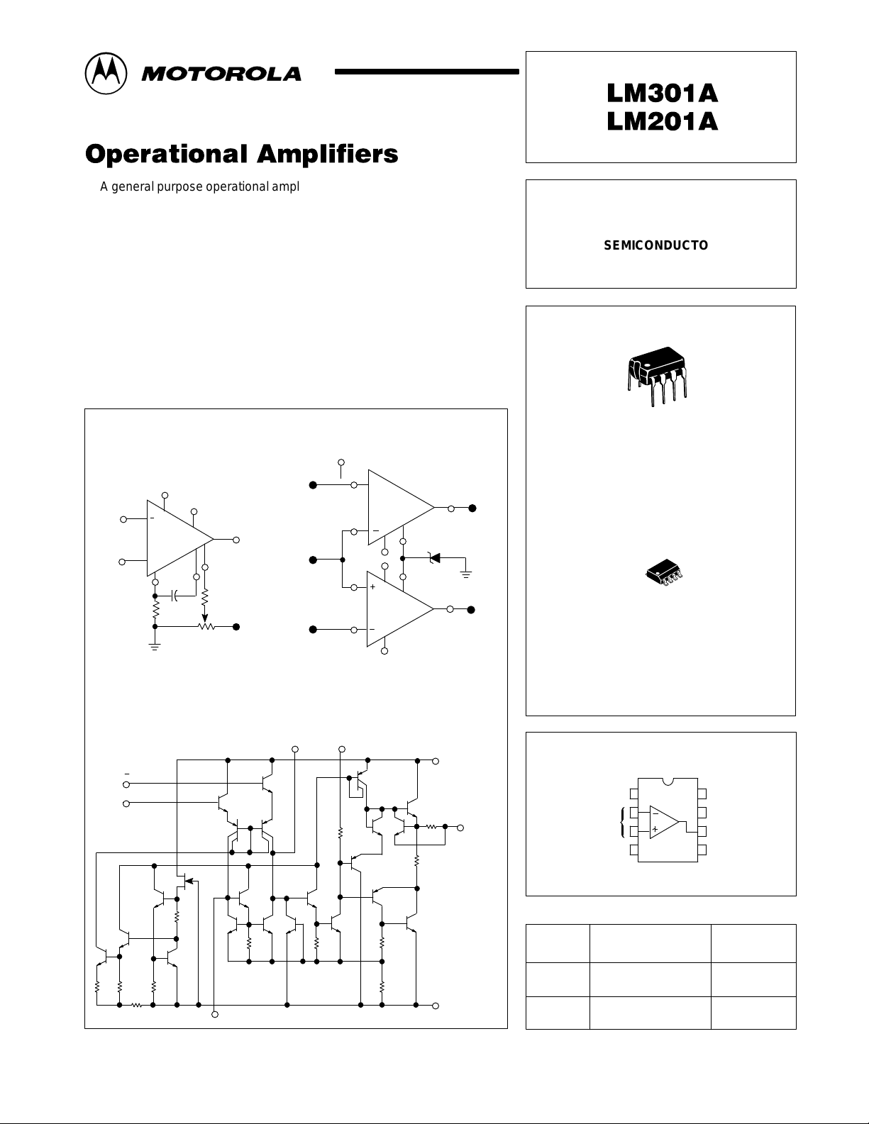
Figure 1. Standard
Compensation and
Offset Balancing Circuit
V
EE
Inverting
Input
Non–
Inverting
Input
Balance
10 M
Ω
+
Freq
Compen
30 pF
V
CC
Balance
5.1 M
20 k
Output
Ω
V
EE
Figure 2. Double–Ended
Limit Detector
V
V
UT
V
V
CC
+
VO = 4.8 V for
VLT
VO = –0.4 V
V
EE
VI < VLT or VI > V
MZ4622 or Equiv.
3.9 V
≤
VI ≤ V
UT
I
LT
V
EE
V
CC
(Pins Not Shown Are Not Connected)
VO
VO
UT
Order this document by LM301A/D
OPERATIONAL AMPLIFIERS
SEMICONDUCTOR
TECHNICAL DATA
8
1
N SUFFIX
PLASTIC PACKAGE
CASE 626
8
1
D SUFFIX
PLASTIC PACKAGE
CASE 751
(SO–8)
Figure 3. Representative Circuit Schematic
Balance Compensation
Inputs
+
450
40 k40 k
10 k20 k5 k
250
Balance
MOTOROLA ANALOG IC DEVICE DATA
500
80 k
1.0 k
50
25
V
CC
Output
PIN CONNECTIONS
1
Balance
2
Inputs
3
4
EE
(Top View)
8
Compensation
7
V
CC
6
Output
5
BalanceV
ORDERING INFORMATION
Operating
Device
LM301AD
LM301AN
V
EE
LM201AD
LM201AN
Motorola, Inc. 1996 Rev 5
Temperature Range
TA = 0° to +70°C
TA = –25° to +85°C
Package
SO–8
Plastic DIP
SO–8
Plastic DIP
1
Page 2
LM301A LM201A
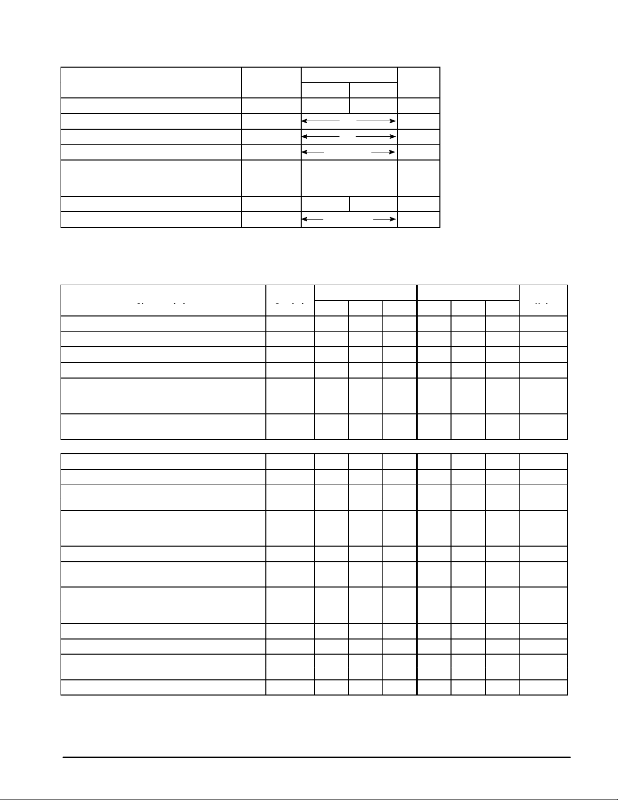
MAXIMUM RATINGS
Value
Rating Symbol LM201A LM301A Unit
Power Supply Voltage V
Input Differential Voltage V
Input Common Mode Range (Note 1) V
Output Short Circuit Duration t
Power Dissipation (Package Limitation) P
Plastic Dual–In–Line Package (LM201A/ 625 625 mW
Derate above TA = +25°C 301A) 5.0 5.0 mW/°C
Operating Ambient Temperature Range T
Storage Temperature Range T
NOTE: 1. For supply voltages less than ±15 V, the absolute maximum input voltage is equal to the supply voltage.
CC, VEE
ID
ICR
SC
D
A
stg
±22 ±18 Vdc
±30 V
±15 V
Continuous
–25 to +85 0 to +70 °C
–65 to +150 °C
ELECTRICAL CHARACTERISTICS (T
supply voltages from ±5.0 V to ±20 V for the LM201A, and from ±5.0 V to ±15 V for the LM301A.
Characteristic Symbol
Input Offset Voltage (RS ≤ 50 kΩ) V
Input Offset Current I
Input Bias Current I
Input Resistance r
Supply Current ICC,I
VCC/VEE = ±20 V – 1.8 3.0 – – –
VCC/VEE = ±15 V – – – – 1.8 3.0
Large Signal Voltage Gain A
(VCC/VEE = ±15 V, VO = ±10 V, RL > 2.0 kΩ)
The following specifications apply over the operating temperature range.
Input Offset Voltage (RS ≤ 50 kΩ) V
Input Offset Current I
Avg Temperature Coef ficient of Input Offset Voltage ∆VIO/∆T – 3.0 15 – 6.0 30 µV/°C
TA(min) ≤ TA ≤ TA (max)
Avg Temperature Coef ficient of Input Of fset Current ∆IIO/∆T nA/°C
+25°C ≤ TA ≤ TA (max) – 0.01 0.1 – 0.01 0.3
TA(min) ≤ TA ≤ 25°C – 0.02 0.2 – 0.02 0.6
Input Bias Current I
Large Signal Voltage Gain A
(VCC/VEE = ±15 V, VO = ±10V, RL > 2.0 kΩ)
Input Voltage Range V
VCC/VEE = ±20 V –15 – +15 – – –
VCC/VEE = ±15 V – – – –12 – +12
Common Mode Rejection (RS ≤ 50 kΩ) CMR 80 96 – 70 90 – dB
Supply Voltage Rejection (RS ≤ 50 kΩ) PSR 80 96 – 70 96 – dB
Output Voltage Swing V
(VCC/VEE = ±15 V, RL = ±10 kΩ, RL > 2.0 kΩ) ±10 ±13 – ±10 ±13 –
Supply Currents (TA = TA(max), VCC/VEE = ±20 V) ICC,I
= +25°C, unless otherwise noted.) Unless otherwise specified, these specifications apply for
A
LM201A LM301A
Unit
IO
IO
IB
i
V
IO
IO
IB
VOL
ICR
O
EE
EE
Min Typ Max Min Typ Max
– 0.7 2.0 – 2.0 7.5 mV
– 1.5 10 – 3.0 50 nA
– 30 75 – 70 250 nA
1.5 4.0 – 0.5 2.0 – MΩ
50 160 – 25 160 – V/mV
– – 3.0 – – 10 mV
– – 20 – – 70 nA
– – 100 – – 300 nA
25 – – 15 – – V/mV
±12 ±14 – ±12 ±14 – V
– 1.2 2.5 – – – mA
mA
V
2
MOTOROLA ANALOG IC DEVICE DATA
Page 3

LM301A LM201A
Figure 4. Minimum Input V oltage Range Figure 5. Minimum Output V oltage Swing
20
Applicable to the Specified
16
12
8.0
, INPUT VOLTAGE RANGE (V)
4.0
IR
V
Operating Temperature
Ranges
Positive
Negative
0
0 5.0 10 15 20
VCC, ( –VEE), SUPPLY VOLTAGE (V) VCC, ( –VEE), SUPPLY VOLTAGE (V)
Figure 6. Minimum V oltage Gain Figure 7. T ypical Supply Currents
100
Applicable to the Specified
94
Operating Temperature
Ranges
LM201A
only
20
±
16
12
8.0
4.0
, OUTPUT VOL TAGE RANGE ( V)
OR
V
2.5
2.0
Applicable to the Specified
Operating Temperature
Ranges
Minimum
RL = 10 k
Minimum
RL = 2.0 k
0
0 5.0 10 15 20
LM201A
only
88
82
, VOLTAGE GAIN (dB)
V
76
A
70
VCC, ( –VEE), SUPPLY VOLTAGE (V) VCC, ( –VEE), SUPPLY VOLTAGE (V)
Figure 8. Open Loop Frequency Response Figure 9. Large Signal Frequency Response
180
160
140
120
100
80
60
40
, VOLTAGE GAIN (dB)
V
A
20
0
–20
1.0 10 100 1.0 k 10 k 100 k 1.0 M 10 M
Single–Pole Compensation
C1 = 3.0 pF
C1 = 30 pF
Gain
f, FREQUENCY (Hz) f, FREQUENCY (Hz)
Phase
LM201A
only
315
270
225
180
135
90
45
0
1.5
LM201A
1.0
, SUPPLY CURRENTS (mA)II,
0.5
CC EE
0
0 5.0 10 15 200 5.0 10 15 20
±
15
10
5.0
, OUTPUT VOL TAGE RANGE ( V)
OR
V
0
1.0 k 10 k 100 k 1.0 M 10 M
TA = +25°C
Single–Pole Compensation
C1 = 3.0 pF
C1 = 30 pF
only
MOTOROLA ANALOG IC DEVICE DATA
3
Page 4

Figure 10. V oltage Follower Pulse Response Figure 11. Open Loop Frequency Response
10
8.0
V)
±
6.0
4.0
2.0
0
–2.0
VOLTAGE RANGE (
,
–4.0
OR
–6.0
, V
IR
V
–8.0
–10
0 102030405060708090
Figure 12. Large Signal Frequency Response Figure 13. Inverter Pulse Response
18
±
16
12
8.0
4.0
, OUTPUT VOL TAGE RANGE ( V)
OR
V
0
Single–Pole Compensation
Input
t, TIME (µs)
Feedforward
Compensation
f, FREQUENCY (Hz)
LM301A LM201A
Output
140
120
100
80
60
40
, VOLTAGE GAIN (dB)
20
V
A
0
–20
10 100 1.0 k 10 k 100 k 1.0 M 10 M 100 M
10
8.0
±
6.0
4.0
2.0
0
–2.0
–4.0
–6.0
, OUTPUT VOL TAGE RANGE ( V)
–8.0
OR
V
–10
0 1.0 2.0 3.0 4.0 5.0 6.0 7.0 8.0 9.01.0 M 10 M100 k
Feedforward
Compensation
Gain
f, FREQUENCY (Hz)
Feedforward
Compensation
Input
t, TIME (
µ
Phase
s)
Output
225
180
135
90
45
PHASE LAG (DEGREES)
0
0
Figure 14. Single–Pole Compensation Figure 15. Feedforward Compensation
C2
R2
2
3
150 pF
+
R2
7
1
V
CC
4
Balance
C2 =
fo = 3.0 MHz
6
V
EE
VO
1
π
foR2
2
V
7
CC
6
+
8
4
V
1
EE
Compensation
C1
C1
Cs = 30 pF
VO
Frequency
R1 C
s
≥
R1 +R2
V
R1
I
R3 C1
MOTOROLA ANALOG IC DEVICE DATA
–VI
+V
R1
R3
I
2
3
Balance
4
Page 5

NOTE 2
–T–
SEATING
PLANE
H
58
–B–
14
F
–A–
C
N
D
K
G
0.13 (0.005) B
M
T
LM301A LM201A
OUTLINE DIMENSIONS
N SUFFIX
PLASTIC PACKAGE
CASE 626–05
(LM201A and LM301A)
ISSUE K
L
J
M
M
A
M
NOTES:
1. DIMENSION L TO CENTER OF LEAD WHEN
FORMED PARALLEL.
2. PACKAGE CONTOUR OPTIONAL (ROUND OR
SQUARE CORNERS).
3. DIMENSIONING AND TOLERANCING PER ANSI
Y14.5M, 1982.
DIM MIN MAX MIN MAX
A 9.40 10.16 0.370 0.400
B 6.10 6.60 0.240 0.260
C 3.94 4.45 0.155 0.175
D 0.38 0.51 0.015 0.020
F 1.02 1.78 0.040 0.070
G 2.54 BSC 0.100 BSC
H 0.76 1.27 0.030 0.050
J 0.20 0.30 0.008 0.012
K 2.92 3.43 0.115 0.135
L 7.62 BSC 0.300 BSC
M ––– 10 ––– 10
N 0.76 1.01 0.030 0.040
INCHESMILLIMETERS
__
C
A
E
B
A1
D SUFFIX
PLASTIC PACKAGE
CASE 751–05
(SO–8)
ISSUE R
D
58
0.25MB
1
H
4
e
M
h
X 45
_
q
C
A
SEATING
PLANE
0.10
L
B
SS
A0.25MCB
NOTES:
1. DIMENSIONING AND TOLERANCING PER ASME
Y14.5M, 1994.
2. DIMENSIONS ARE IN MILLIMETERS.
3. DIMENSION D AND E DO NOT INCLUDE MOLD
PROTRUSION.
4. MAXIMUM MOLD PROTRUSION 0.15 PER SIDE.
5. DIMENSION B DOES NOT INCLUDE MOLD
PROTRUSION. ALLOWABLE DAMBAR
PROTRUSION SHALL BE 0.127 TOTAL IN EXCESS
OF THE B DIMENSION AT MAXIMUM MATERIAL
CONDITION.
MILLIMETERS
DIM MIN MAX
A 1.35 1.75
A1 0.10 0.25
B 0.35 0.49
C 0.18 0.25
D 4.80 5.00
E
3.80 4.00
1.27 BSCe
H 5.80 6.20
h
0.25 0.50
L 0.40 1.25
0 7
q
__
MOTOROLA ANALOG IC DEVICE DATA
5
Page 6

LM301A LM201A
Motorola reserves the right to make changes without further notice to any products herein. Motorola makes no warranty , representation or guarantee regarding
the suitability of its products for any particular purpose, nor does Motorola assume any liability arising out of the application or use of any product or circuit, and
specifically disclaims any and all liability, including without limitation consequential or incidental damages. “T ypical” parameters which may be provided in Motorola
data sheets and/or specifications can and do vary in different applications and actual performance may vary over time. All operating parameters, including “Typicals”
must be validated for each customer application by customer’s technical experts. Motorola does not convey any license under its patent rights nor the rights of
others. Motorola products are not designed, intended, or authorized for use as components in systems intended for surgical implant into the body, or other
applications intended to support or sustain life, or for any other application in which the failure of the Motorola product could create a situation where personal injury
or death may occur. Should Buyer purchase or use Motorola products for any such unintended or unauthorized application, Buyer shall indemnify and hold Motorola
and its officers, employees, subsidiaries, affiliates, and distributors harmless against all claims, costs, damages, and expenses, and reasonable attorney fees
arising out of, directly or indirectly, any claim of personal injury or death associated with such unintended or unauthorized use, even if such claim alleges that
Motorola was negligent regarding the design or manufacture of the part. Motorola and are registered trademarks of Motorola, Inc. Motorola, Inc. is an Equal
Opportunity/Affirmative Action Employer.
How to reach us:
USA/EUROPE/Locations Not Listed: Motorola Literature Distribution; JAP AN: Nippon Motorola Ltd.; Tatsumi–SPD–JLDC, 6F Seibu–Butsuryu–Center,
P.O. Box 20912; Phoenix, Arizona 85036. 1–800–441–2447 or 602–303–5454 3–14–2 Tatsumi Koto–Ku, Tokyo 135, Japan. 03–81–3521–8315
MFAX: RMF AX0@email.sps.mot.com – TOUCHT ONE 602–244–6609 ASIA/PACIFIC: Motorola Semiconductors H.K. Ltd.; 8B Tai Ping Industrial Park,
INTERNET: http://Design–NET.com 51 Ting Kok Road, Tai Po, N.T., Hong Kong. 852–26629298
6
◊
MOTOROLA ANALOG IC DEVICE DATA
LM301A/D
*LM301A/D*
 Loading...