

Page 1
LM2005 20 Watt Automotive Power Amplifier
LM2005 20 Watt Automotive Power Amplifier
April 1989
General Description
The LM2005 is a dual high power amplifier, designed to
deliver optimum performance and reliability for automotive
applications. High current capability (3.5A) enables the device to deliver 10W/channel into 2X (LM2005T-S), or 20W
bridged monaural (LM2005T-M) into 4X, with low distortion.
Features
Y
Wide supply range (8V –18V)
Y
Externally programmable gain
Y
With or without bootstrap
Y
Low distortion
Y
Low noise
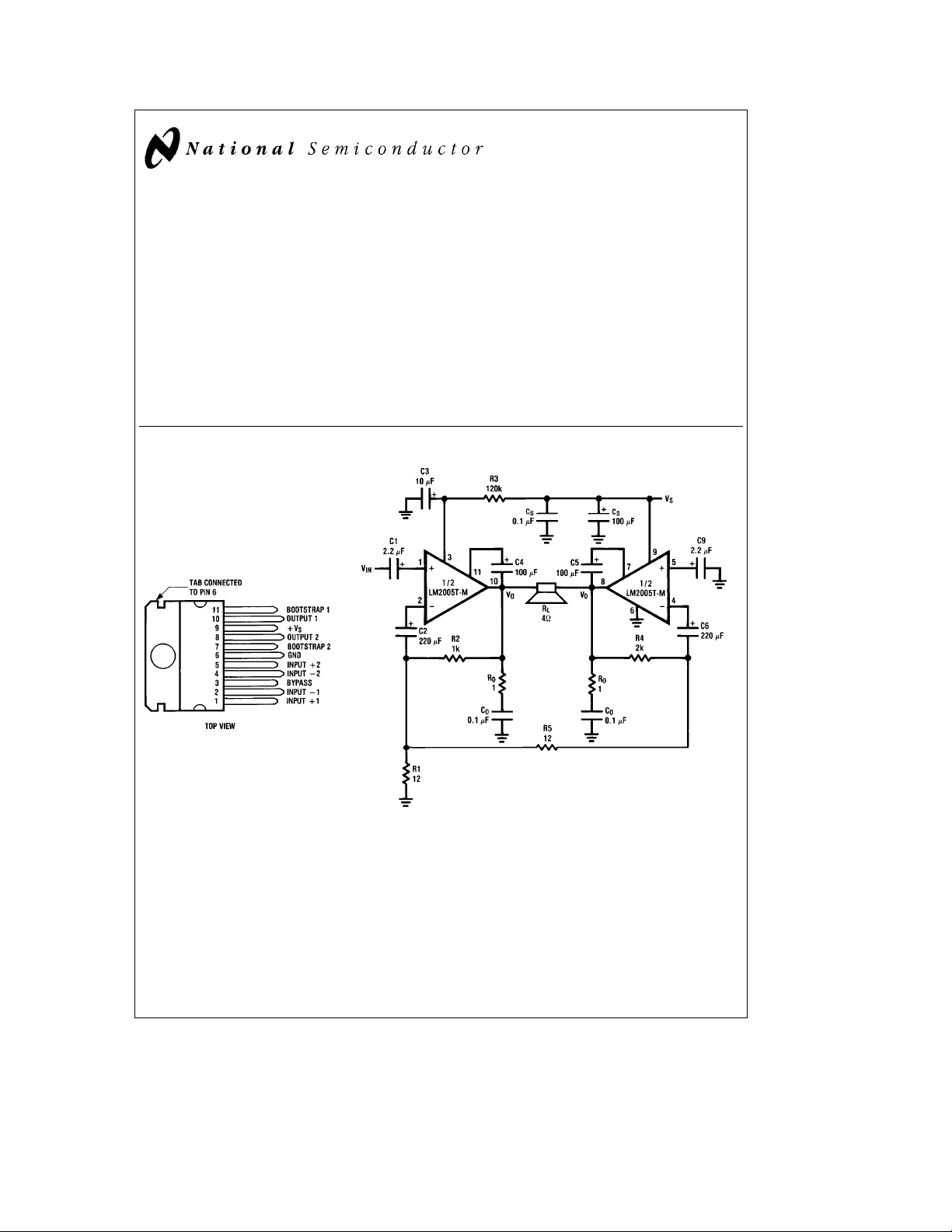
Connection Diagram
Plastic Package
Typical Application
Y
High peak current capability
Y
e
P
20W bridge
O
Y
High voltage protection
Y
AC and DC output short circuit protection to ground or
across load
Y
Thermal protection
Y
Inductive load protection
Y
Accidental open ground protection
Y
Immunity to 40V power supply transients
Y
3§C/W device dissipation
Y
Pin for pin compatible with TDA2005
TL/H/5129– 1
Order Number LM2005T-S
or LM2005T-M
See NS Package Number TA11A
TL/H/5129– 2
FIGURE 1. 20W Bridge Amplifier Application and Test Circuit
C
1995 National Semiconductor Corporation RRD-B30M115/Printed in U. S. A.
TL/H/5129
Page 2
LM2005T-M and LM2005T-S
Absolute Maximum Ratings
If Military/Aerospace specified devices are required,
please contact the National Semiconductor Sales
Office/Distributors for availability and specifications.
Operating Supply Voltage 18V
DC Supply Voltage (Note 1) 28V
Peak Supply Voltage (50 ms) 40V
Output Current
Repetitive (Note 2) 3.5A
Non-Repetitive 4.5A
Power Dissipation 30W
Operating Temperature
Storage Temperature
b
40§Ctoa85§C
b
60§Ctoa150§C
Lead Temp. (Soldering, 10 seconds) 260
C
§
LM2005T-M
Electrical Characteristics
R
th (heatsink)
e
4§C/W, unless otherwise specified
Refer to the bridge application circuit,
Figure 1
,T
amb
e
Parameter Test Conditions Min Typ Max Units
Supply Voltage 818V
Output Offset Voltage (Note 3) V
(between Pin 8 and 10) V
Total Quiescent Drain Current V
Includes Current in Feedback Resistors V
e
14.4V
S
e
13.2V
S
e
14.4V R
S
e
13.2V R
S
g
e
4X 75 150 mA
L
e
3.2X 70 160 mA
L
Output Power de10% fe1 kHz
e
V
S
e
V
S
14.4V R
13.2V R
e
4X 18 20 W
L
e
R
3.2X 20 22 W
L
e
3.2X 17 19 W
L
THD fe1 kHz
e
V
14.4V R
S
e
P
50 mW to 15W 1 %
O
e
V
13.2V R
S
e
P
50 mW to 13W 1 %
O
e
4X
L
e
3.2X
L
Input Sensitivity fe1 kHz
e
P
2W R
O
e
P
2W R
O
e
4X 9mV
L
e
3.2X 8mV
L
Input Resistance fe1 kHz 70 kX
Low Frequency Roll Off (b3 dB) R
High Frequency Roll Off (b3 dB) R
e
3.2X 40 Hz
L
e
3.2X 20 kHz
L
Closed Loop Voltage Gain fe1 kHz 45 50 dB
Total Input Noise Voltage R
Supply Voltage Rejection R
Efficiency V
Output Voltage with One Side V
of the Speaker Shorted to Ground V
Note 1: Internal voltage limit. Shuts down above 20V.
Note 2: Internal current limit.
Note 3: For LM2005T-M only.
Note 4: Bandwidth filter: 22 Hz to 22 kHz.
e
10 kX (Note 4) 3 10 mV
g
e
10 kX f
g
e
C
10 mFV
4
e
14.4V fe1 kHz
S
e
P
20W R
O
e
P
22W R
O
e
V
13.2V fe1 kHz
S
e
P
19W R
O
e
14.4V R
S
e
13.2V R
S
e
100 Hz
ripple
e
0.5V
ripple
e
4X 60 %
L
e
3.2X 60 %
L
e
3.2X 58 %
L
e
4X
L
e
3.2V
L
45 55 dB
25§C, A
20
e
50 dB,
V
g
150 mV
g
150 mV
2V
2
Page 3
LM2005T-S
Electrical Characteristics
R
th (heatsink)
e
4§C/W, unless otherwise specified
Refer to the stereo application circuit,
Figure 2,
e
T
amb
Parameter Test Conditions Min Typ Max Units
Supply Voltage 818V
Quiescent Output Voltage V
Total Quiescent Drain Current V
Includes Current in Feedback Resistors V
e
14.4V 6.6 7.2 7.8 V
S
e
V
13.2V 6 6.6 7.2 V
S
e
14.4V 65 120 mA
S
e
13.2V 62 120 mA
S
Output Power fe1 kHz de10%
(Each Channel) V
e
14.4V R
S
e
V
13.2V R
S
e
V
16V R
S
e
4X 6 6.5 W
L
e
R
3.2X 78 W
L
e
R
2X 910 W
L
e
R
1.6X 10 11 W
L
e
3.2X 6 6.5 W
L
e
R
1.6X 910 W
L
e
2X 12 W
L
THD fe1 kHz
(Each Channel) V
Cross Talk V
(Note 5) R
e
14.4V R
S
e
P
50 mW to 4W 0.2 1 %
O
e
V
14.4V R
S
e
P
50 mW to 6W 0.3 1 %
O
e
V
13.2V R
S
e
P
50 mW to 3W 0.2 1 %
O
e
V
13.2V R
S
e
P
40 mW to 6W 0.3 1 %
O
e
14.4V
S
e
4X
L
e
V
4V
O
rms
e
R
5kX
g
e
4X
L
e
2X
L
e
3.2X
L
e
1.6X
L
e
f
1 kHz 40 60 dB
fe10 kHz 40 dB
Input Saturation Voltage 300 mV
Input Sensitivity fe1 kHz P
e
1W
O
e
R
4X 6
L
e
R
3.2X 5.5
L
Input Resistance fe1 kHz Non-Inverting Input 70 200 kX
Inverting Input 10 kX
Low Frequency Roll Off (b3 dB) R
High Frequency Roll Off (b3 dB) R
e
2X 50 Hz
L
e
2X 15 kHz
L
Voltage Gain (Open Loop) fe1 kHz 90 dB
Voltage Gain (Closed Loop) fe1 kHz 48 50 51 dB
Closed Loop Gain Matching 0.5 dB
Total Input Noise Voltage R
Supply Voltage Rejection R
Efficiency V
Note 5: For LM2005T-S only.
Note 6: Bandwidth filter: 22 Hz to 22 kHz.
e
10 kX (Note 6) 1.5 5 mV
g
e
10 kX f
g
e
C
10 mFV
3
e
14.4V fe1 kHz
S
e
R
4X P
L
e
R
2X P
L
e
V
13.2V fe1 kHz
S
e
R
3.2X P
L
e
R
1.6X P
L
e
100 Hz
ripple
e
0.5V
ripple
e
6.5W 70 %
O
e
10W 60 %
O
e
6.5W 70 %
O
e
10W 60 %
O
35 45 dB
25§C, G
e
50 dB,
v
mV
3
Page 4

Equivalent Schematic
TL/H/5129– 3
4
Page 5

External Components
(Figure 2)
Components Comments
1. R1, R2 Sets voltage gain,
R5, R4
R
Ê
j
a
1
e1a
for one channel,
R1
R
Ê
for the other.
R5
A
V
A
V
Where R’ is the equivalent resistance
of R2 in parallel with an internal 10k
resistor:
10k#R2
R2a10k
.
e
R
Ê
If R2m10k, then
R2
.
j
a
1
A
V
R1
2. R3 Adjusts output symmetry for maximum
power output.
3. R
O,CO
Works to stabilize internal output
stage. Necessary for stability. C
should be ceramic disc or equivalently
O
good high frequency capacitor.
4. C1, C9 Input coupling capacitor. Low
frequency pole set by
e
1
F
L
2qZ (non-inverting) C1
1
.
Decreasing capacitor value will also
increase noise.
Typical Applications (Continued)
Components Comments
5. C4, C5 Bootstrap capacitors, used to increase
drive to output stage.
6. C3 Improves power supply rejection.
Increasing C3 increases turn-on delay
(approximately 2 ms per mF).
7. C2, C6 Inverting input DC decouple. Low
frequency pole:
e
F
2
L
2qZ(inverting)C2
1
.
Z (inverting)&10 kX.
8. C
C
Output coupling capacitor. Isolates
pins 10 and 8 from load. Low
frequency pole;
1
2qRLC
.
C
9. C
e
3
F
L
S
Power supply filtering.
FIGURE 2. 10W/Channel Stereo Amplifier Application and Test Circuit
5
TL/H/5129– 4
Page 6

Typical Performance Characteristics
Device Dissipation vs
Ambient Temperature
Supply Current vs
Supply Voltage
Output Offset Voltage vs
Supply Voltage
Power Output vs
Supply Voltage
Total Harmonic Distortion
vs Power Output (Bridge)
Channel Separation
(Referred to the Output)
vs Frequency
Output Swing vs
Supply Voltage
Total Harmonic Distortion
vs Power Output (Dual)
Total Harmonic Distortion
vs Frequency (Dual)
Power Supply Rejection
Ratio (Referred to the
Output) vs Frequency
Power Output vs Supply
Voltage
TL/H/5129– 5
6
Page 7

Application Hints
The high current capability of the LM2005 allows it to continuously endure either AC or DC short circuit of the output
with a maximum supply voltage of 16V. This will protect the
loudspeaker in a bridge mode, when a DC short of the output occurs on one side of the speaker. The device will prevent the speaker from destruction by reducing the DC
across the load (bridge mode) to typically less than 2
e
V
method.
DC(VS
14.4V, R
The LM2005 can withstand a constant 28 V
with no damage (maximum operating voltage is 18V). The
device is also protected from load dump or dangerous transients up to 40V for 50 ms (every 1000 ms) on the supply
with no damage.
Protection diodes protect the device driving inductive loads,
during which the load can generate voltages greater than
e
4X), by an internal current pullback
L
on the supply
DC
supply or less than ground levels. The protection diodes will
clamp these transients to a safe V
rails.
The bridge configuration in
Figure 3
above and below the
BE
is designed for applications requiring minimal printed circuit board area and maximum cost effectiveness. The circuit will function with the
elimination of bootstrap components R3, C4 and C5 (refer
to
Figure 1
). This will result in less output power by decreasing output voltage swing to the load. By using internal feedback resistors (typically 10 kX), feedback components R2,
R3 and C2 (
Figure 1
) may be omitted where closed loop
voltage gain accuracy is not critical. The net result is a stable, cost effective circuit that will satisfy many application
needs.
e
A
41.5 dB@1 kHz FIGURE 3. Minimal Component Application Circuit
V
Component Side (Scale 2:1)
FIGURE 4. Printed Circuit Board Layout for LM2005
TL/H/5129– 6
TL/H/5129– 7
7
Page 8

Physical Dimensions inches (millimeters) Lit.
LM2005 20 Watt Automotive Power Amplifier
Ý
107847
11-Lead TO-220 Power Package (T)
Order Number LM2005T-S or LM2005T-M
NS Package Number T11A
LIFE SUPPORT POLICY
NATIONAL’S PRODUCTS ARE NOT AUTHORIZED FOR USE AS CRITICAL COMPONENTS IN LIFE SUPPORT
DEVICES OR SYSTEMS WITHOUT THE EXPRESS WRITTEN APPROVAL OF THE PRESIDENT OF NATIONAL
SEMICONDUCTOR CORPORATION. As used herein:
1. Life support devices or systems are devices or 2. A critical component is any component of a life
systems which, (a) are intended for surgical implant support device or system whose failure to perform can
into the body, or (b) support or sustain life, and whose be reasonably expected to cause the failure of the life
failure to perform, when properly used in accordance support device or system, or to affect its safety or
with instructions for use provided in the labeling, can effectiveness.
be reasonably expected to result in a significant injury
to the user.
National Semiconductor National Semiconductor National Semiconductor National Semiconductor
Corporation Europe Hong Kong Ltd. Japan Ltd.
1111 West Bardin Road Fax: (
Arlington, TX 76017 Email: cnjwge@tevm2.nsc.com Ocean Centre, 5 Canton Rd. Fax: 81-043-299-2408
Tel: 1(800) 272-9959 Deutsch Tel: (
Fax: 1(800) 737-7018 English Tel: (
National does not assume any responsibility for use of any circuitry described, no circuit patent licenses are implied and National reserves the right at any time without notice to change said circuitry and specifications.
Fran3ais Tel: (
Italiano Tel: (
a
49) 0-180-530 85 86 13th Floor, Straight Block, Tel: 81-043-299-2309
a
49) 0-180-530 85 85 Tsimshatsui, Kowloon
a
49) 0-180-532 78 32 Hong Kong
a
49) 0-180-532 93 58 Tel: (852) 2737-1600
a
49) 0-180-534 16 80 Fax: (852) 2736-9960
 Loading...