

Page 1
February 1998
LM1296
Raster Geometry Correction System for Multi-Frequency
Displays
General Description
The LM1296 is a monolithic IC for use in the raster scanning
circuitry of a multi-frequency CRT monitor. The IC provides
an S-corrected sawtooth waveformandavariable DC output
voltage. These two outputs drive the vertical deflection amplifier. It also provides another waveform for East-West geometry correction which includes pincushion, corner, and
trapezoid controls. The geometry correction is controlled by
DC input voltages from 0V to 4V.
The raster height and the raster vertical position can be controlled by two DC voltage input pins that adjust the sawtooth
waveform amplitude and the variable DC output voltage. The
East-West correction of the LM1296 has height tracking and
vertical position tracking capabilities. As the height or position of the raster is adjusted the geometry correction is maintained by the chip automatically.
The LM1296 is packaged in a 16-pin plastic DIP package.
Features
n Vertical scanning frequency 50 Hz–165 Hz
n Accepts either polarity of V sync
n DC-controlled correction terms
n Raster vertical position control
n Vertical S-correction (linearity) control
n East-West pincushion control
n East-West trapezoid control
n East-West corner control
n Provides both polarities of correction output
n East-West correction tracks raster vertical position and
height
n Compatible with LM1290 and LM1292 horizontal PLL
Applications
n Vertical deflection of monitors
LM1296 Raster Geometry Correction System for Multi-Frequency Displays
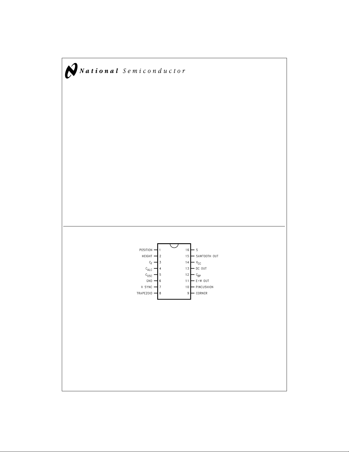
Connection Diagram
DS012894-1
FIGURE 1.
Order Number LM1296N
See NS Package Number N16A
© 1998 National Semiconductor Corporation DS012894 www.national.com
Page 2
Absolute Maximum Ratings (Notes 3, 1)
If Military/Aerospace specified devices are required,
please contact the National Semiconductor Sales Office/
Distributors for availability and specifications.
Supply Voltage (V
Input Voltage (V
Pins 1, 2, 8, 9, 10, 16 0V ≤ V
Power Dissipation (P
Above 25˚C, Derate
Based on θ
Thermal Resistance (θ
Junction Temperature (T
) 15V
CC
)
IN
)
D
and TJ(Note 4) 1.5W
JA
) 81˚C/W
JA
) 150˚C
JMAX
≤ 5V
IN
ESD Susceptibility (Note 5) 2 kV
Storage Temperature −65˚C to +150˚C
Lead Temperature (Soldering 10 sec.) 265˚C
Operating Ratings(Note 2)
Supply Voltage (V
Input Voltage (V
Pins 1, 2, 8, 9, 10, 16 0V ≤ V
Output Current (I
Pins 11, 13, 15 −2 mA ≤ I
Temperature Range (T
) 10.8V ≤ VCC≤ 13.2V
CC
)
IN
)
OUT
) 0˚C to +70˚C
A
OUT
≤ 4V
IN
≤ 2mA
Electrical Characteristics
See Test Circuit (
Figure 2
), V
=
CC
Symbol Parameter Conditions Min Typ Max Units
I
CC
Supply Current Pins 11, 13, 15 Loaded, 2mA 26 32 mA
V SYNC Vertical Sync Input Sensitivity (Pin 7) 1%or 99%Duty Cycle
f
f
f
R
R
R
R
V
V
k
MIN
MAX
FR
IN1
IN2
IN3
IN4
O15
DC15
TEMP
Minimum Lock Frequency C
Maximum Lock Frequency C
Free Run Frequency V
Input Resistance (Pin 1) 25 kΩ
Input Resistance (Pin 2) V
Input Resistance (Pins 8, 9, 10) 50 kΩ
Input Resistance (Pin 16) 50 kΩ
SAWTOOTH OUT (Pin 15) V
Output Amplitude (R
L15
SAWTOOTH OUT (Pin 15) V
Output DC Voltage (R
L15
SAWTOOTH OUT (Pin 15) (Note 9) 1.5
Temperature Stability
k
S
V
RDCV
S-Correction of Sawtooth Output (Pin 15) V
Relative DC Voltage between V
DC OUT (Pin 13) and V
SAWTOOTH OUT (Pin 15)
=
V
V
RDCV
13−VDC15
=
(R
5kΩ)
V
TRAP
L13
Trapezoid Correction V
Output Waveform Amplitude V
(Pin 11, R
V
PIN
Pincushion Correction V
=
5kΩ) Pincushion and Corner
L11
Output Waveform Amplitude V
(Pin 11, R
=
5kΩ) Trapezoid and Corner
L11
12V; V
=
2
4V; V
=
4V; V
16
Rectangular Waveform 1 V
AC-Coupled to Pin 7
Through 0.01 µF Cap.
=
OSC
=
OSC
=
4V or 0V 40 Hz
7
=
1V 12 kΩ
2
=
4V, V
=
5kΩ)V
=
5kΩ)
2
=
4V, V
2
=
V
0V, V
2
=
V
0V, V
2
=
0V to 4V, V
2
=
4V, V
2
=
V
4V, V
2
=
4V −200 mV
1
=
1.5V 200
1
=
4V, V
2
=
4V, V
2
Corrections are Null
=
4V, V
2
=
4V, V
2
Corrections are Null
RDCV
=
0V (Note 6); T
=
25˚C unless otherwise specified
A
(Note 8) (Note 7) (Note 8)
0.15 µF 50 Hz
0.15 µF 165 Hz
=
0V 1.8
16
=
4V 3.1 V
16
=
0V 1
16
=
4V 1.7
16
=
0V to 4V 3.9 V
16
=
4V 0.5
16
=
0V 2
16
=
0V 0.87 V
8
=
4V 0.73
8
=
0V 1.9 V
10
=
4V 1.45
10
%
%
PP
PP
PP
PP
www.national.com 2
Page 3
Electrical Characteristics (Continued)
See Test Circuit (
Figure 2
), V
=
CC
Symbol Parameter Conditions Min Typ Max Units
V
CNR
Corner Correction V
Output Waveform Amplitude V
(Pin 11, R
V
DC11
E-W OUT Trapezoid, Pincushion, and 4.1 V
=
5kΩ) Trapezoid and Pincushion
L11
Output Offset Voltage Corner Correction Waveforms
(Pin 11, R
Note 1: Absolute Maximum Ratings indicate limits beyond which damage to the device may occur.
Note 2: Operating Ratings indicate conditions for which the device is functional, but do not guarantee specific performance limits. For guaranteed specifications and
test conditions, see the Electrical Characteristics. The guaranteed specifications apply only for the test conditions listed. Some performance characteristics may degrade when the device is not operated under the listed test conditions.
Note 3: All voltages are measured with respect to GND, unless otherwise specified.
Note 4: The maximum power dissipation must be derated at elevated temperatures and is dictated by T
allowable power dissipation at any elevated temperature is P
this device, T
Note 5: Human Body model, 100 pF capacitor discharged through a 1.5 kΩ resistor.
Note 6: Adjust V
Note 7: Typical specifications are specified at T
Note 8: Tested limits are guaranteed to National’s AOQL (Average Outgoing Quality Level).
Note 9: Amplitude stability versus ambient temperature is defined by |V
at 70˚C and 25˚C respectively.
JMAX
1
=
5kΩ) are Null
L11
=
150˚C. The typical thermal resistance (θ
RDCV
=
0V, where V
until V
12V; V
=
2
4V; V
=
4V; V
16
RDCV
=
4V, V
2
=
4V, V
2
Corrections are Null
=
D
) of the LM1296 is 81˚C/W.
JA
=
V
RDCV
13−VDC15
=
25˚C and represent most likely parametric norm.
A
)/θJAor the number given in the Absolute Maximum Ratings, whichever is lower. For
(T
JMAX–TA
.
|/V25x 100%, where V70and V25are the output sawtooth peak-to-peak amplitudes
70−V25
=
0V (Note 6); T
=
25˚C unless otherwise specified
A
(Note 8) (Note 7) (Note 8)
=
0V 1.1 V
9
=
4V 0.8
9
, θJAand the ambient temperature, TA. The maximum
JMAX
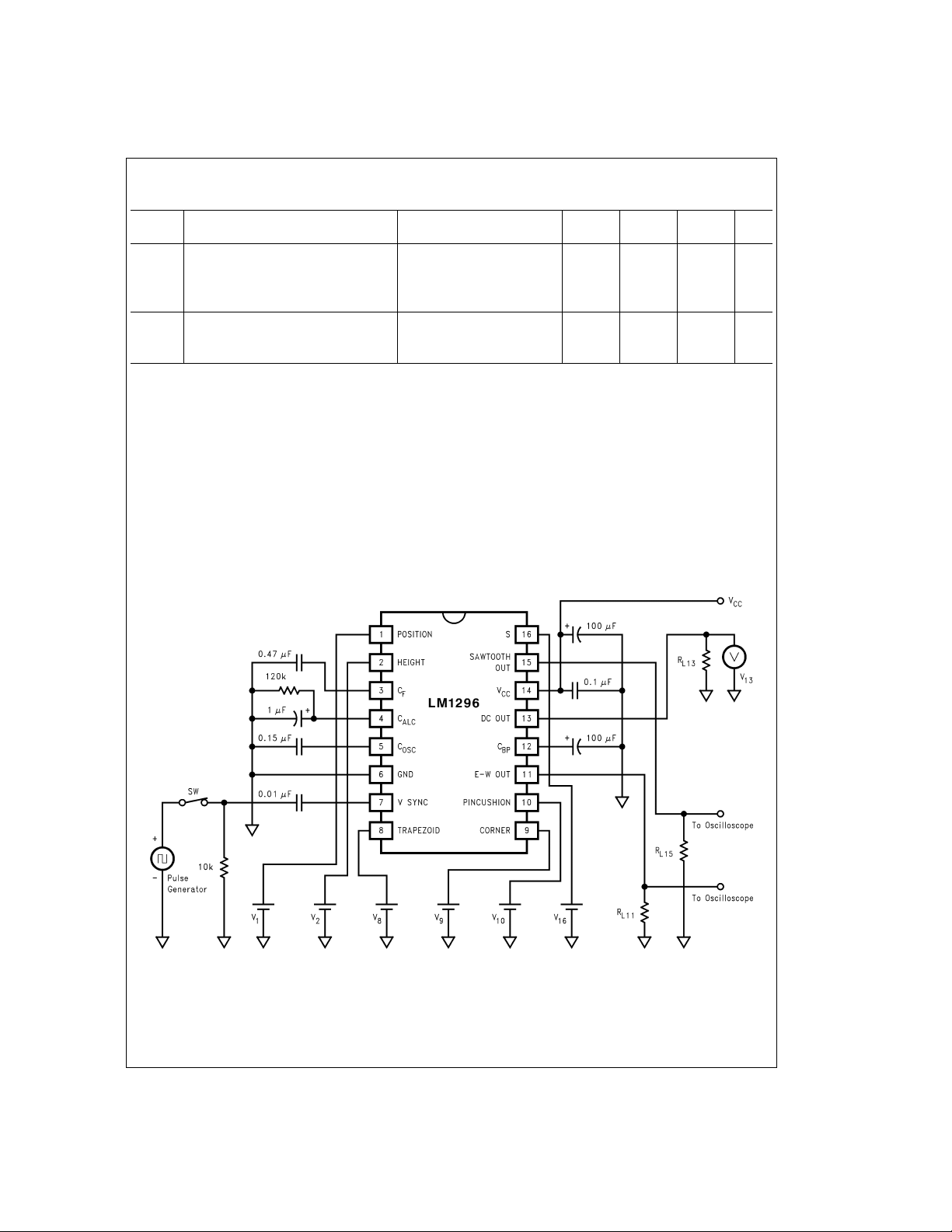
Test Circuit
PP
FIGURE 2.
Typical Performance Characteristics
=
T
A
25˚C, f
=
v
60 Hz, V
=
2
4V, V
=
4V, V
16
RDCV
=
0V, V
8,9,10
DS012894-2
=
Set for null correction waveforms, unless otherwise specified
3 www.national.com
Page 4

Typical Performance Characteristics (Continued)
E-W Out (Pin 11)
E-W Out (Pin 11)
DS012894-3
DS012894-5
E-W Out (Pin 11)
DS012894-4
E-W Out (Pin 11)
DS012894-6
E-W Out (Pin 11)
DS012894-7
www.national.com 4
E-W Out (Pin 11)
DS012894-8
Page 5

Block Diagram
Functional Description
The LM1296 outputs a sawtooth and a variable DC voltage
for the vertical deflection amplifier. It also provides the horizontal deflection output circuit with a waveform for Trapezoid, Pincushion and Corner correction.
Referring to
larity Correction Block that accepts either positive-going or
negative-going sync signals. The polarity-corrected sync is
sent to the Injection-Locked Oscillator so that the sawtooth
generated is synchronized with the vertical sync. With no
sync signal AC-coupled to pin 7, the oscillator free runs at
typically 40 Hz.
There are three capacitors and one control pin connected to
the Sawtooth Waveform Generation Block. C
ing capacitor for the Injection-Locked Oscillator. C
ter capacitor for an internal circuit that detects the existence
of vertical sync and prevents the Injection-Locked Oscillator
from locking at twice the vertical sync frequency. C
the automatic level control (ALC) circuit. The ALC circuit
maintains the sawtooth output amplitude, which is set by the
DC voltage at pin 2 (HEIGHT), regardless of the vertical sync
frequency. Since the output sawtooth goes to the geometry
correction circuit as well, the correction waveform generated
tracks the sawtooth amplitude, i.e., the height of the CRT
raster.
The S Correction block shapes the linear sawtooth into an
S-shape sawtooth. Pin 15 (SAWTOOTH OUT) outputs the
buffered S-shape sawtooth. The amount of S correction is
controlled by the DC voltage at pin 16 (S).
Figure 3
, pin 7 (V SYNC) goes to the Sync Po-
OSC
is the tim-
is the fil-
F
is for
ALC
FIGURE 3.
Referring to
Figure 4
, the extent of S correction is defined by
the following equation.
=
k
S
+ ∆A2)/2A x 100
(∆A
1
FIGURE 4.
The LM1296 is designed to drive an external vertical deflection amplifier that is operating with positive and negative
power supplies. The LM1296 outputs an S-corrected sawtooth with a DC level that is typical 3.85V. Pin 13 (DC OUT)
±
provides a DC voltage of 3.85V
200 mV. By applying a DC
control voltage to pin 1 (POSITION), the output voltage at pin
13 can be varied. This sets the output DC current from the
vertical deflection amplifier, which in turn sets the raster vertical position.
DS012894-9
%
DS012894-10
5 www.national.com
Page 6

Functional Description (Continued)
Pin 1 (POSITION) not only controls the pin 13 output, but
also the center position of the correction waveform at pin 11
(E-W OUT). As a result, the geometry correction tracks the
vertical position of the CRT raster. See
ure 7
.
Figure 5
through
Fig-
The Pincushion Control Block and the Corner Control Block
are non-linear analog circuits. They convert the sawtooth
waveform into 2nd order and 4th order parabolic waveforms.
These two parabolic waveforms, together with a sawtooth
(1st order), are summed and then buffered out at pin 11
(E-W OUT). See waveforms in the Typical Performance
Characteristics section. The amplitudes of the 1st, 2nd and
4th order components in the correction waveform are controlled by the DC voltages at pin 8 (TRAPEZOID), pin 9
(CORNER) and pin 10 (PINCUSHION).
DS012894-11
FIGURE 5. Raster Position Centered
Pin Descriptions
See
Figure 8
through
matics.
Figure 13
Pin 1. POSITION: A 0V to 4V DC voltage applied to this pin
sets pin 13 (DC OUT) output voltage from 3.65V to 4.05V.
See
Figure 8
for the input schematic.
Pin 2. HEIGHT: A 0V to 4V DC voltage applied to this pin
sets the output amplitude of the sawtooth waveform at pin 15
(SAWTOOTH OUT) as well as the output amplitude of the
correction waveform at pin 11 (E-W OUT). See
the input schematic.
Pin 3. C
: A 0.47 µF capacitor is connected from this pin to
F
ground. This capacitor prevents the Injection-Locked Oscillator from locking at twice the V sync frequency.
Pin 4. C
circuit (ALC) is connected from this pin to ground. The ALC
: A filter capacitor for the automatic level control
ALC
circuit maintains the output amplitudes of SAWTOOTH OUT
and E-W OUT regardless of the V sync frequency. The recommended capacitance of C
Pin 5. C
cillator is connected from this pin to ground. The recom-
: A timing capacitor for the Injection-Locked Os-
OSC
mended capacitance is 0.15 µF. Increasing the capacitance
will lower the lowest lock frequency.
Pin 6. GND: Ground pin.
Pin 7. V SYNC: This pin accepts AC-coupled V sync of ei-
ther polarity. See
Figure 10
sensitivity of this pin is about 1 V
a resistor of 10 kΩ in parallel with a filter capacitor of 0.01 µF
should be connected from the input side of the coupling capacitor to ground. The values of these components may be
for input and output sche-
Figure 9
for
is between 1 µF to 4.7 µF.
ALC
for the input schematic.The input
. For best noise immunity,
PP
DS012894-12
FIGURE 6. Raster Position Up
DS012894-13
FIGURE 7. Raster Position Down
varied depending on the application and the ambient noise
level inside the monitor.A DC voltage of 0V or 4V on this pin
will cause the device to free run at about 40 Hz.
Pin 8. TRAPEZOID: A 0V to 4V DC voltage applied to this
pin adjusts the polarity and the amount of linear sawtooth
component (Trapezoid Correction) in the E-W OUT output.
At approximately 2V, the amount is zero. Avoltage above 2V
sets a negative-sloped sawtooth output, increasing the voltage increases the sawtooth amplitude. A voltage below 2V
sets a positive-sloped sawtooth output, decreasing the voltage increases the sawtooth amplitude. See
Figure 11
for the
input schematic.
Pin 9. CORNER: A 0V to 4V DC voltage applied to this pin
adjusts the polarity and the amount of 4th order parabolic
component (Corner Correction) in the E-W OUT output. At
approximately 2V, the amount is zero. A voltage above 2V
sets a concave down 4th order output, increasing the voltage
increases the 4th order amplitude. A voltage below 2V sets a
concave up 4th order output, decreasing the voltage increases the 4th order amplitude. See
Figure 11
for the input
schematic.
Pin 10. PINCUSHION: A 0V to 4V DC voltage applied to this
pin adjusts the polarity and the amount of 2nd order parabolic component (Puncushion Correction) in the E-W OUT
output. At approximately 2V, the amount is zero. A voltage
above 2V sets a concave down 2nd order output, increasing
the voltage increases the 2nd order amplitude. A voltage below 2V sets a concave up 2nd order output, decreasing the
voltage increases the 2nd order amplitude. See
Figure 11
for
the input schematic.
www.national.com 6
Page 7

Pin Descriptions (Continued)
Pin 11. E-W OUT: The output waveform at this pin consists
of the sum of the linear sawtooth, 2nd order parabolic and
4th order parabolic waveform components. The center position of the output waveform tracks the output voltage at pin
13 (DC OUT). See
Pin 12. C
BP
this pin to ground via a short path.
Figure 12
for the output schematic.
: A capacitor of at least 100 µF is connected from
Pin 13. DC OUT: This pin outputs a variable DC voltage from
3.65V to 4.05V.The output voltage is controlled by the control voltage at pin 1 (POSITION). See
Figure 12
for the out-
put schematic.
Input/Output Schematics
Pin 14. V
be decoupled to pin 6 (GND) via a short path with a capacitor
: 12V nominal power supply pin. This pin should
CC
of at least 100 µF.
Pin 15. SAWTOOTH OUT: This pin outputs an S-corrected
sawtooth waveform with the amplitude controlled by pin 2
(HEIGHT). See
Figure 12
for the output schematic.
Pin 16: S: A 0V to 4V DC voltage applied to this pin adjusts
the amount of S correction in the sawtooth waveform at pin
15 (SAWTOOTH OUT). 0V sets maximum S correction. See
Figure 13
for the input schematic.
FIGURE 8.
FIGURE 9.
FIGURE 10.
DS012894-14
DS012894-15
DS012894-16
DS012894-17
FIGURE 11.
DS012894-18
FIGURE 12.
DS012894-19
FIGURE 13.
7 www.national.com
Page 8

Typical Application
DS012894-20
www.national.com 8
* Actual values depend on the application and the ambient noise level inside the monitor.
Page 9

9
Page 10

Physical Dimensions inches (millimeters) unless otherwise noted
16-Lead (0.300" Wide) Molded Dual-In-Line Package
Order Number LM1296N
NS Package Number N16A
LIFE SUPPORT POLICY
NATIONAL’S PRODUCTS ARE NOT AUTHORIZED FOR USE AS CRITICAL COMPONENTS IN LIFE SUPPORT DE-
LM1296 Raster Geometry Correction System for Multi-Frequency Displays
VICES OR SYSTEMS WITHOUT THE EXPRESS WRITTEN APPROVAL OF THE PRESIDENT OF NATIONAL SEMICONDUCTOR CORPORATION. As used herein:
1. Life support devices or systems are devices or systems which, (a) are intended for surgical implant into
the body, or (b) support or sustain life, and whose failure to perform when properly used in accordance
2. A critical component in any component of a life support
device or system whose failure to perform can be reasonably expected to cause the failure of the life support
device or system, or to affect its safety or effectiveness.
with instructions for use provided in the labeling, can
be reasonably expected to result in a significant injury
to the user.
National Semiconductor
Corporation
Americas
Tel: 1-800-272-9959
Fax: 1-800-737-7018
Email: support@nsc.com
www.national.com
National Semiconductor
Europe
Fax: +49 (0) 1 80-530 85 86
Email: europe.support@nsc.com
Deutsch Tel: +49 (0) 1 80-530 85 85
English Tel: +49 (0) 1 80-532 78 32
Français Tel: +49 (0) 1 80-532 93 58
Italiano Tel: +49 (0) 1 80-534 16 80
National Semiconductor
Asia Pacific Customer
Response Group
Tel: 65-2544466
Fax: 65-2504466
Email: sea.support@nsc.com
National Semiconductor
Japan Ltd.
Tel: 81-3-5620-6175
Fax: 81-3-5620-6179
National does not assume any responsibility for use of any circuitry described, no circuit patent licenses are implied and National reserves the right at any time without notice to change said circuitry and specifications.
 Loading...