

Page 1
LM1295
DC Controlled Geometry Correction System for
Continuous Sync Monitors
LM1295 DC Controlled Geometry Correction System for Continuous Sync Monitors
April 1999
General Description
The LM1295 is specifically designed for use in a continuous
sync monitor. The injection-locked vertical oscillator operates from 50 Hz to 170 Hz, covering all known video monitors. A differential output current is provided in order to prevent ground interaction.
The IC provides two outputs composed of the summation of
DC controlled 1st and 2nd order output terms. The first output corrects for EW pincushion and trapezoid. The second
corrects for parallelogram and bow.
A DCcontrolled output is provided for vertical dynamic focus
correction.
The IC is packaged in a 24-pin narrow DIP package and operates on a single 12V power supply.
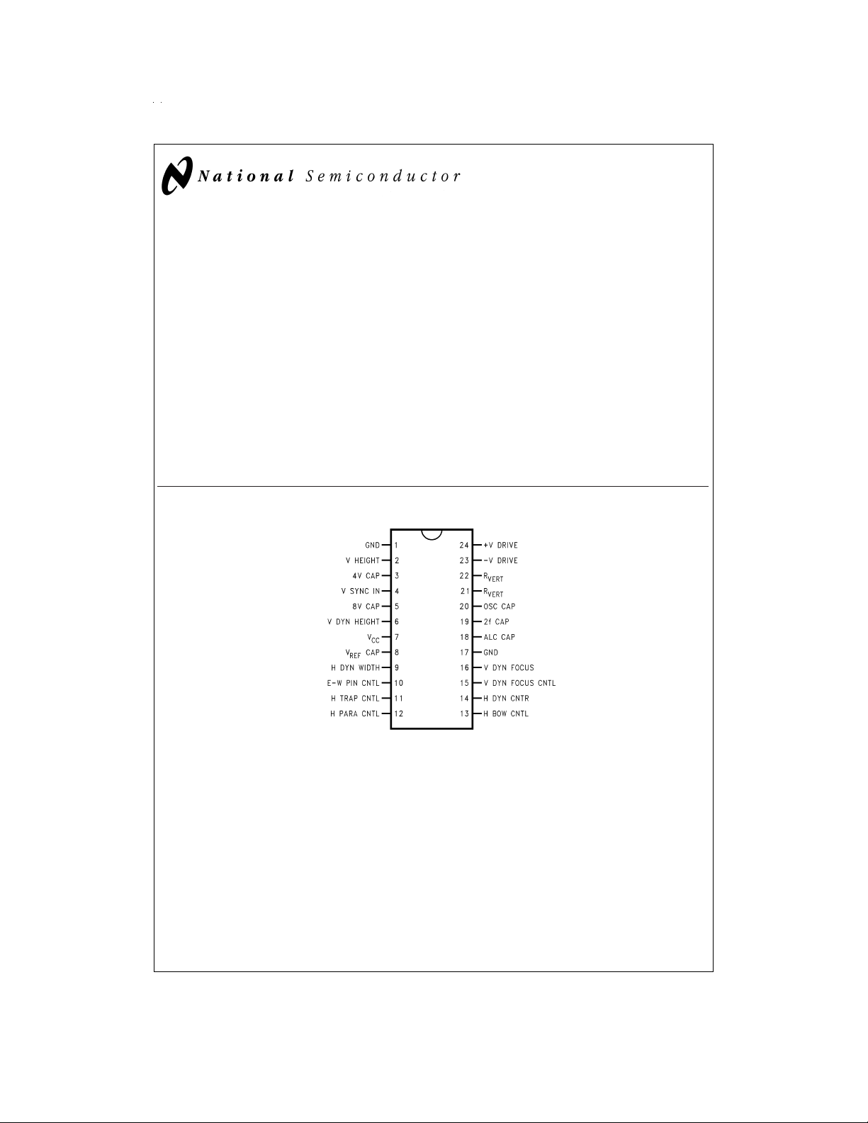
Connection Diagram
Features
n Vertical scanning frequency 50 Hz–170 Hz
n DC controlled correction term amplitudes
n Up to 125 kHz bandwidth for dynamic input signals
n Minimum external parts count
n Multiple IC connection for convergence applications
flexibility
n Stable vertical amplitude over temperature
n Compatible with the LM1291 Horizontal PLL in a H/V
system
n Dynamic vertical deflection correction for second anode
high voltage drop
n Both positive and negative going correction signals
DS012324-1
FIGURE 1. Order Number LM1295N
See NS Package Number N24C
© 1999 National Semiconductor Corporation DS012324 www.national.com
Page 2
Absolute Maximum Ratings (Notes 1, 3)
If Military/Aerospace specified devices are required,
please contact the National Semiconductor Sales Office/
Distributors for availability and specifications.
Supply Voltage 15V
Input Voltage
(DC, pins 2, 4, 6, 10, 11, 12, 13, 15) 5V
Input Voltage (AC, Pin 4) 5 V
Power Dissipation (Note 4)
(Above 25˚C Derate Based on
and TJ) 1.8W
θ
JA
Thermal Resistance (θ
Junction Temperature (T
) 70˚C/W
JA
) 150˚C
J
ESD Susceptibility (Note 5) 1.8 kV
Storage Temperature −65˚C to +150˚C
Lead Temperature (Soldering, 10 sec.) 265˚C
Operating Ratings (Note 2)
Operating Temperature Range −20˚C to +80˚C
PP
Supply Voltage (V
Input Voltage
(DC, pins 2, 4, 6, 10, 11, 12,
13, 15) 4V
Input Voltage
(AC, pin 4) 4 V
) 10.8V ≤ VCC≤ 13.2V
CC
PP
Electrical Characteristics
See Test Circuit (
Figure 2
); T
A
=
25˚C; V
Symbol Parameter Conditions
I
CC
V
R
F
FR
F
max
Supply Current All Control Inputs=3V
Internal Ref Voltage at Pin 8 8.2 V
REF
Input Resistance Pins 6, 10–13, 15
IN
Free-Run Frequency 45 Hz
Maximum Frequency 170 Hz
Cntlbw Control Inputs Bandwidth Pins 6, 10–13, 15 125 kHz
V
V
V
V
V
V
V
V
V
CR
CR
CP
Vertical Height Temperature
HTS
Stability
Vertical Differential Output Current V Height=4V, V Dyn Height=4V,
DIFF
V Sync High Input Voltage 2.4 V(min)
SYNH
V Sync Low Input Voltage
SYNL
Vertical Output CMRR V
CMRR
Vertical Output PSSR V
PSRR
Vertical Peak Output Voltage R
OP-P
Vertical Ramp Distortion (Note 8) V Height=4V,
RERR
Vertical Parabola Distortion (Note 9) V Height=2.2V, F=100 Hz,
SOERR
First Order (Ramp) Correction,
FO
H Dyn Cntr (Pin 14)
First Order (Ramp) Correction,
FO
H Dyn Width (Pin 19)
Parabola Correction Range,
SO
H Dyn Cntr (Pin 14),
H Dyn Width (Pin 9),
V Dyn Focus (Pin 16)
=
12V.
CC
V Height=4V, V Dyn Height=3V,
=
F=100 Hz, T
0˚C to 70˚C (Note 9)
A
Pin 24 Minus Pin 23
=
1V to 4V, V Height=2V,
O
V Dyn Height=3V
=
10.8V to 13.2V, V Height=2V,
CC
V Dyn Height=3V
=
10k
L
V Dyn Height=3V
V Dyn Height=3V
Pin 12=0V
Pin 12=4V
V Dyn Height=3V, V Height=4V,
Parabola Nulled
Pin 11=0V
Pin 11=4V
V Dyn Height=3V, V Height=4V,
Parabola Nulled
Pins 10, 13, 15=0V
Pins 10, 13, 15=4V
V Dyn Height=3V, V Height=4V,
Ramp Nulled for H Dyn Cntr and H Dyn
Width
Typical
(Note 6)
Limit
(Note 7)
25 35
50 30
1
1 mA(min)
0.8
30 dB
30 dB
65
1
8
2.50
2.25
0.85
0.75
1.2
1.0
Units
mA
(max)
kΩ
(min)
%
V
(max)
V
(min)
%
%
V
V
V
PP
PP
PP
PP
www.national.com 2
Page 3
Electrical Characteristics (Continued)
See Test Circuit (
Figure 2
); T
A
=
25˚C; V
Symbol Parameter Conditions
V
I
O
Output DC Bias Pins 9, 14 and 16; All Control
ODC
Output Current Pins 9, 14 and 16 5.0 mA
Note 1: Absolute Maximum Ratings indicate limits beyond which damage to the device may occur.
Note 2: Operating Ratings indicate conditions for which the device is functional, but do not guarantee specific performance limits. For guaranteed specifications and
test conditions, see the Electrical Characteristics. The guaranteed specifications apply only for the test conditions listed. Some performance characteristics may degrade when the device is not operated under the listed test conditions.
Note 3: All voltages are measured wIth respect to GND, unless otherwise specified.
Note 4: The maximum power dissipation must be derated at elevated temperatures and is dictated by T
allowable power dissipation at any temperature is P
=
T
150˚C. The typical thermal resistance (θ
Jmax
Note 5: Human body model, 100 pF capacitor discharged through a 1.5 kΩ resistor.
Note 6: Typicals are at T
Note 7: Tested limits are guaranteed to National’s AOQL (Average Outgoing Quality Level).
Note 8: The deviation from a straight line drawn through measured points at 5%and 95%of the ramp is used to calculate distortion.
Distortion=100 (deviation, volts)/(95%value − 5%value, volts). Deviations are measured at
Note 9: The deviation from a theoretical parabola drawn through the apex of the actual parabola is used to calculate distortion.
Distortion=100 (deviation, volts)/(theoretical parabola, volts) at measuring point. Nine points are measured.
Note 10: The amplitude stability versus temperature is typically 1%or less at 100 Hz when a standard 10k 5
21 and 22 and located close to the package. The negative temperature coefficient of the resistor corrects for the negative temperature coefficient of the LM1295. The
typical amplitude stability of the LM1295 by itself is 2%.
=
=
T
25˚C and represent most likely parametric norm.
A
J
=
12V.
CC
Inputs at 2.2V
=
D
) of these parts when board mounted follow: LM1295N 70˚C/W.
JA
)/θJAor the number given in the Absolute Maximum Ratings, whichever is lower. For this device,
(T
Jmax−TA
Jmax
1
⁄3and2⁄3of the ramp time period.
Typical
(Note 6)
Limit
(Note 7)
4.0 V
, θJAand the ambient temperature, TA. The maximum
1
%
⁄4W carbon film resistor is connected between pins
Units
DC
www.national.com3
Page 4
Test Circuit
FIGURE 2.
Typical Performance Characteristics
DS012324-2
=
T
25˚C, V
A
Height
=
0V to 4V, V
Dyn Height
=
3V
Lowest Lock Frequency vs OSC Cap
Graph 1
www.national.com 4
DS012324-12
Page 5

Typical Performance Characteristics T
Circuit—
Figure 2
=
25˚C, F=100 Hz, V
A
Height
=
4V, V
Dyn Height
=
3V, Test
H Dyn Width Output (Pin 9)
H Dyn Width Output (Pin 9)
DS012324-10
DS012324-13
H Dyn Width Output (Pin 9)
DS012324-11
H Dyn Width Output (Pin 9)
DS012324-14
H Dyn Ctr Output (Pin 14)
DS012324-15
H Dyn Ctr Output (Pin 14)
DS012324-16
www.national.com5
Page 6

Typical Performance Characteristics T
Figure 2
Circuit—
(Continued)
=
25˚C, F=100 Hz, V
A
Height
=
4V, V
Dyn Height
=
3V, Test
H Dyn Cntr Output (Pin 14)
V Dyn Focus Output (Pin 16)
DS012324-17
H Dyn Cntr Output (Pin 14)
DS012324-18
V Dyn Focus Output (Pin 16)
DS012324-19
−V Drive Output (Pin 23)
DS012324-21
Circuit Description
(See
Figure 3
, Block Diagram)
The LM1295 has outputs which provide signals for correcting the following CRT distortions: Vertical de-focusing,
East-West pincushion, horizontal trapezoid, horizontal paral-
www.national.com 6
DS012324-20
+V Drive Output (Pin 24)
DS012324-22
lelogram and horizontal bow. The amount and polarity of the
corrections are controlled by voltages between 0V and 4V.
The corrections track the vertical output amplitude.
The LM1295 has five major sections: the vertical oscillator/
amplifier, the parabolic function generator and three
voltage-controlled channels with the correction term outputs.
Page 7

Circuit Description (Continued)
VERTICAL OSCILLATOR
The vertical oscillator is an injection-locked ramp generator
with automatic level control. The automatic level control
maintains the oscillator output ramp height with changes in
input frequency. The oscillator requires negative-going TTL
level vertical sync pulses, wider than 200 ns, to lock. In the
absence of vertical sync, the oscillator runs at free-run frequency.The vertical output amplitude is controlled by a voltage between 0V and 4V on the V Height input with a range
of about 1.8 to 1, and by a voltage between 3V and 4V on the
Vertical Dynamic Height input with a range of about 1.3 to 1.
The control bandwidth of the V Height input is low due to the
automatic level control, but that of the Vertical Dynamic
Height is greater than 125 kHz. The oscillator has a circuit,
requiring an external capacitor, 2f Cap, that prevents the oscillator from locking at twice the vertical sync frequency.The
oscillator ramp voltage is converted into differential currents
superimposed on DC currents of about 315 µA for each output. The voltage to current conversion gain is inversely proportional to the value of the resistor connected between the
Rvert pins (21 and 22). Differential current outputs are provided instead of voltage to avoid ground noise. The ramp
voltage goes to the parabolic function generator and to two
multipliers used as voltage controlled amplifiers, one for horizontal trapezoid correction and the other for horizontal parallelogram correction.
PARABOLIC FUNCTION GENERATOR
The parabolic function generator makes a parabolic waveform from the vertical ramp. Its output goes to three multipliers used as voltage controlled amplifiers, one each for V Dyn
Focus, E-W Pin, and H Bow.
VOLTAGE CONTROLLED AMPLIFIERS
The V Dyn Focus voltage controlled amplifier is controlled by
the V Dyn Focus Cntl input. Its output goes to an op amp
whose output is V Dyn Focus. The voltage controlled amplifier has zero gain at approx. 2V input, maximum positive
gain at 4V, and maximum negative gain at 0V. The E-W Pin,
H Bow, H Trap and H Para voltage controlled amplifiers are
identical to the V Dyn Focus stage, each adjusted by its corresponding Cntl input. The bandwidth of the Cntl inputs is
greater than 125 kHz. The E-W Pin and H Bow amplifiers
have the parabolic waveform as their input, and the H Trap
and H Para amplifiers have the vertical ramp as their input.
The parabolic waveform and the ramp amplitudes track the
vertical output amplitude so the correction amplitudes follow
accordingly.The outputs of the E-W Pin amplifier (parabola)
and the H Trap amplifier (ramp) are summed together in an
op amp summing circuit, with H Trap weight
Pin. The output of the summing amplifier is H Dyn Width,
used for correcting E-W pincushion and horizontal trapezoid
distortion. The outputs of the H Bow amplifier (parabola) and
the H Para amplifier (ramp) are summed together similarly,
with H Bow and H Para equally weighted. The output of the
summing amplifier is H Dyn Cntr, used for correcting horizontal bow and horizontal parallelogram distortion. All three
op amp outputs are identical structures and are typical low
output impedance type op amp outputs, capable of sinking
or sourcing 5 mA minimum.
1
⁄3that of E-W
Block Diagram
DS012324-3
FIGURE 3.
www.national.com7
Page 8

Pin Descriptions
See
Figure 4
through
Figure 8
ics.
GND (Pin 1): This pin should be connected to the power
ground at pin 17.
V Height (Pin 2): Vertical Height. A voltage between 0V and
4V on this pin controls the amplitude of the +V and −V Drive
currents, with increasing voltage giving increasing current.
The control range is approximately 1.8 to 1. The response
time is slow,being limited by the automatic level control loop.
4 V Cap (Pin 3): 4 Volt Cap Capacitor. A 10 µF capacitor,
aluminum electrolytic or tantalum, should be connected between pin 3 (positive side) and GND (pin 17) to bypass the
internal 4V reference.
V Sync In (Pin 4): Vertical Sync Input. The vertical sync input takes a negative-going TTL level pulse which injection
locks the vertical oscillator to the vertical sync frequency if it
is above the LM1295 minimum frequency. The input threshold level is approximately 2V, so pulses other than TTL level
are satisfactory as long as they cross the 2V threshold with
at least a 400 mV margin either side. The minimum pulse
width is approximately 200 ns. For free-running detection (no
V Sync in), this input should be at logic high.
8 V Cap (Pin 5): 8 Volt Capacitor. A 100 µF capacitor, aluminum electrolytic or tantalum, should be connected between
pin 5 (positive side) and GND (pin 17) to bypass the internal
8V reference.
V Dyn Height (Pin 6): Vertical Dynamic Height. A voltage
between 3V and 4V on this pin controls the amplitude of the
+V and −V Drive currents with increasing voltage giving increasing current. The control range is approximately
1.3 to 1. The bandwidth of this input is DC to greater than
125 kHz in contrast to the slow Vertical Height input.
V
(Pin 7): Power, 12V nominal. VCCshould be bypassed
CC
to GND (pin 17) with a 10 µF aluminum electrolytic or tantalum capacitor.
VrefCap (Pin 8): VoltageReference Cap. A 10 µF capacitor,
aluminum electrolytic or tantalum, should be connected between pin 8 (positive side) and GND (pin 17).
H Dyn Width (Pin 9): Horizontal Dynamic Width. This output
consists of the sum of the vertical ramp and the parabola derived from the ramp. The amplitude and polarity of the ramp
signal is DC controlled by H Trap Cntl (pin 11) and of the parabola by E-W Pin Cntl (pin 10). The weighting of the ramp is
1
⁄3the parabola; i.e., with the H Trap and E-W Pin Cntls at
4V,theoutput is 3 parts parabola and 1 part ramp. Horizontal
Dynamic Width is used to correct for trapezoid and east-west
pincushion distortion. The output stage is similar to a standard op-amp output. The bandwidth from either of the 2 control pins to the output is DC to greater than 125 kHz.
E-W Pin Cntl (Pin 10): East-West Pincushion Control. A
voltage of 0V to 4V adjusts the polarity and the amount of
parabola in the Horizontal Dynamic Width (pin 9) output. At
approximately 2V, the amount is zero. From 2V to 4V, the
amplitude increases and the parabola is positive-going.
From 2V to 0V, the amplitude increases and the parabola is
negative-going.
H Trap Cntl (Pin 11): Horizontal Trapezoid Control. A voltage of 0V to 4V adjusts the polarity and the amount of vertical ramp in the Horizontal Dynamic Width (pin 9) output. At
approximately 2V, the amount is zero. From 2V to 4V, the
amplitude increases and the ramp is positive-going. From 2V
to 0V, the amplitude increases and the ramp is
negative-going.
for Input and Output schemat-
H Para Cntl (Pin 12): Horizontal Parallelogram Control. A
voltage of 0V to 4V adjusts the polarity and the amount of
vertical ramp in the Horizontal Dynamic Center (pin 14) output.At approximately 2V, the amount is zero. From 2V to 4V,
the amplitude increases and the ramp is positive-going.
From 2V to 0V, the amplitude increases and the ramp is
negative-going.
H Bow Cntl (Pin 13): Horizontal Bow Control. A voltage of
0V to 4V adjusts the polarity and the amount of parabola in
the Horizontal Dynamic Center (pin 14) output. At approximately 2V, the amount is zero. From 2V to 4V, the amplitude
increases and the parabola is positive-going. From 2V to 0V,
the amplitude increases and the parabola is negative-going.
H Dyn Cntr (Pin 14): Horizontal Dynamic Center. This output consists of the sum of the vertical ramp and the parabola
derived from the ramp. The amplitude and polarity of the
ramp signal is DC controlled by H Para Cntl (pin 12) and of
the parabola by H Bow Cntl (pin 13). The difference between
this output and the Horizontal Dynamic Width output is in the
weighting of the ramp, which is equal to the parabola; i.e.,
with the H Para and H Bow Cntls at 4V, the output is 1 part
parabola and 1 part ramp. Horizontal Dynamic Center is
used to correct for parallelogram and bow distortion. The
output stage is similar to a standard op-amp output. The
bandwidth from either of the 2 control pins to the output is
DC to greater than 125 kHz.
V Dyn Focus Cntl (Pin 15): Vertical Dynamic Focus Control.Avoltage of 0V to 4V adjusts the polarity and the amount
of parabola in the Vertical Dynamic Focus (pin 16) output. At
approximately 2V, the amount is zero. From 2V to 4V, the
amplitude increases and the parabola is positivegoing. From
2V to 0V, the amplitude increases and the parabola is
negative-going.
V Dyn Focus (Pin 16): Vertical Dynamic Focus. This output
consists of the parabola derived from the vertical ramp. The
amplitude and polarity are controlled by V Dyn Focus Cntl.
The output stage is similar to a standard op-amp output. The
bandwidth from the control pin to the output is DC to greater
than 125 kHz.
GND (Pin 17): Ground. This is the power supply ground for
the 12V supply and the point to which the bypass capacitors
are returned.
ALC Cap (Pin 18): Automatic Level Control Capacitor. This
capacitor is part of the level control circuit that maintains
constant vertical height in spite of vertical sync frequency
changes. The recommended value is 4.7 µF, aluminum electrolytic or tantalum capacitor. If the VCO capacitor value is
changed, this capacitor value should change in the same ratio. A 300k resistor should be connected from this pin to
ground.
2f Cap (Pin 19): Double frequency Capacitor. This capacitor
prevents the vertical oscillator from locking at twice the vertical sync frequency. The recommended value is 0.47 µF. If
the VCO capacitor value is changed, this capacitor value
should change in the same ratio.
Osc Cap (Pin 20): A timing capacitor is connected from this
pin to ground for the internal oscillator. The capacitance determines the lowest lock frequency. See Graph 1.
Rvert (Pin 21): Vertical Resistor.One end of the Vertical Resistor connects to this pin. This resistor determines the gain
of the vertical ramp current generator. The gain is inversely
proportional to the resistance. It is recommended that this be
a standard 5
1
%
⁄4W carbon film resistor whose negative tem-
www.national.com 8
Page 9

Pin Descriptions (Continued)
perature coefficient corrects for the negative temperature coefficient of the LM1295. The resistor should be located near
the LM1295. The recommended value is 10 kΩ.
Rvert (Pin 22): Vertical Resistor. The other end of the Vertical Resistor connects to this pin.
− V Drive (Pin 23): − Vertical Drive. This is the
negative-going vertical ramp output current of the differential
pair.The ramp current waveform is superimposed on a direct
Input/Output Schematics
current of approximately 315 µA. The waveform amplitude is
determined by the Vertical Height (pin 2) control voltage and
the Vertical Dynamic Height (pin 6) control voltage. The current can be converted into voltage by a resistor (typically 10
kΩ) to ground or by a differential amplifier using the differential currents as inputs. The voltage compliance of the output
is typically 6V.
+ V Drive (Pin 24): + Vertical Drive. This is the same as − V
Drive except it is the positive-going output current of the differential pair.
FIGURE 4.
FIGURE 5.
DS012324-4
DS012324-5
DS012324-6
FIGURE 6.
DS012324-7
FIGURE 7.
FIGURE 8.
DS012324-8
www.national.com9
Page 10

Typical Application
Note: LM1295 is designed to drive a differential input vertical deflection amplifier. The LM1295, however, can also drive a single-ended input vertical deflection
amplifier by just using either the +V drive or −V drive pins.
DS012324-9
FIGURE 9.
www.national.com 10
Page 11

Physical Dimensions inches (millimeters) unless otherwise noted
LM1295 DC Controlled Geometry Correction System for Continuous Sync Monitors
24-Lead (0.300" Wide) Molded Dual-In-Line Package
Order Number LM1295N
NS Package Number N24C
LIFE SUPPORT POLICY
NATIONAL’S PRODUCTS ARE NOT AUTHORIZED FOR USE AS CRITICAL COMPONENTS IN LIFE SUPPORT
DEVICES OR SYSTEMS WITHOUT THE EXPRESS WRITTEN APPROVAL OF THE PRESIDENT AND GENERAL
COUNSEL OF NATIONAL SEMICONDUCTOR CORPORATION. As used herein:
1. Life support devices or systems are devices or
systems which, (a) are intended for surgical implant
into the body, or (b) support or sustain life, and
whose failure to perform when properly used in
accordance with instructions for use provided in the
2. A critical component is any component of a life
support device or system whose failure to perform
can be reasonably expected to cause the failure of
the life support device or system, or to affect its
safety or effectiveness.
labeling, can be reasonably expected to result in a
significant injury to the user.
National Semiconductor
Corporation
Americas
Tel: 1-800-272-9959
Fax: 1-800-737-7018
Email: support@nsc.com
www.national.com
National Semiconductor
Europe
Fax: +49 (0) 1 80-530 85 86
Email: europe.support@nsc.com
Deutsch Tel: +49 (0) 1 80-530 85 85
English Tel: +49 (0) 1 80-532 78 32
Français Tel: +49 (0) 1 80-532 93 58
Italiano Tel: +49 (0) 1 80-534 16 80
National Semiconductor
Asia Pacific Customer
Response Group
Tel: 65-2544466
Fax: 65-2504466
Email: sea.support@nsc.com
National Semiconductor
Japan Ltd.
Tel: 81-3-5639-7560
Fax: 81-3-5639-7507
National does not assume any responsibility for use of any circuitry described, no circuit patent licenses are implied and National reserves the right at any time without notice to change said circuitry and specifications.
 Loading...