

Page 1
LM1292
Video PLL System for Continuous-Sync Monitors
LM1292 Video PLL System for Continuous-Sync Monitors
April 1999
General Description
The LM1292 is a very low jitter, integrated horizontal time
base solution specifically designed to operate in high performance, continuous-sync video monitors. It automatically
synchronizes to any H frequency from 22 kHz to 125 kHz
and provides the drive pulse tothehighpower deflection circuit.
Available sync processing includes a vertical sync separator
and a composite video sync stripper. An internal sync selection scheme gives highest priority to separate H and V sync,
then composite sync, and finally sync on video; no external
switching between sync sources is necessary. The LM1292
provides polarity-normalized H/HV and V sync outputs.
The LM1292 design uses an on-chip FVC
(Frequency-to-Voltage Converter) to set the center frequency of the VCO (Voltage-Controlled Oscillator). This
technique allows autosync operation over the entire frequency range using just one optimized set of external components.
The system includes a second phase detector which compensates for storage time variation in the horizontal output
transistor; the picture’s horizontal position is thus independent of temperature and component variance.
The LM1292 provides DC control pins for H Drive duty cycle
and flyback phase.
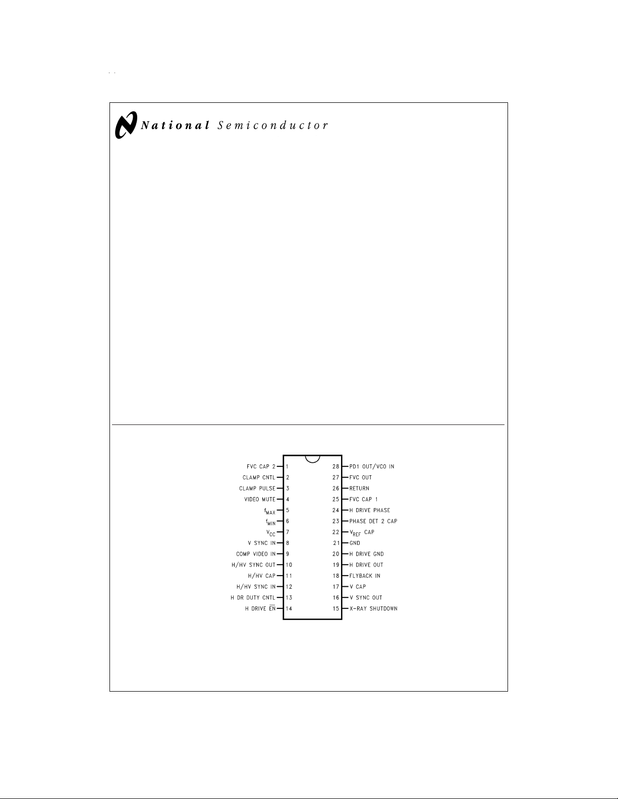
Connection Diagram
Features
n Wide continuous autosync range— 22 kHz–125 kHz
(1:5.7) with no component switching or external
adjustments
n No manufacturing trims required— internal VCO
capacitor trimmed on chip
n No costly high-precision components needed
n Very low phase jitter (below 800 ps at 125 kHz)
n DC controlled H phase and duty cycle
n Video mute pulse for blanking during H frequency
transitions
n Input sync prioritization
n Clamp pulse position and width control
n Continuous clamp pulse output, even with no sync input
n Resistor-programmable minimum and maximum VCO
frequency
n X-ray input disables H drive and mutes video until V
powered down
n H drive disabled for V
n Horizontal output transistor protected against accidental
turn-on during flyback
n Capacitor-programmable frequency ramping, d
protects H output transistor during scanning mode
changes
<
9.5V
CC
CC
f
/dt,
vco
DS012844-1
FIGURE 1. Order Number LM1292N
See NS Package Number N28B
© 1999 National Semiconductor Corporation DS012844 www.national.com
Page 2
Absolute Maximum Ratings (Notes 1, 3)
If Military/Aerospace specified devices are required,
please contact the National Semiconductor Sales Office/
Distributors for availability and specifications.
Supply Voltage 14V
Input Voltage, V
Pin 14
Pin 24
Pins 5, 6
Pins 8, 28
Pins 2, 9, 12, 13, 15, 18
Power Dissipation (PD) 2.5W
(Above 25˚C, derate based on θ
DC
<
1.3V
and TJ)
JA
5V
<
V
7.2V
IN
8V
10V
V
CC
Thermal Resistance (θ
Junction Temperature (T
) 50˚C/W
JA
) 150˚C
J
ESD Susceptibility (Note 5) 2 kV
Storage Temperature −65˚C to +80˚C
Lead Temperature
(Soldering 10 sec.) 265˚C
Operating Ratings (Note 2)
Operating Temperature Range −20˚C to +80˚C
Supply Voltage 10.8V ≤ V
CC
≤ 13.2V
Electrical Characteristics See Test Circuit (
otherwise stated
Parameter Conditions
Supply Current
Minimum Composite Video
Input Amplitude (Pin 9)
Cap Coupled (0.01 µF), Sync Tip to
Black Level
Figure 2
); T
A
=
25˚C; V
=
12V; V
CC
=
0V; V
14
Typical
(Note 6)
30 41
0.14 V
=
15
Limit
(Note 7)
0V unless
Units
(max)
DC Clamp Level, Composite Video Input 2.0 V
Clamp Charging Current, Composite
Video Input
Minimum H/HV Sync Input Amplitude
(Pin 12)
Cap Coupled, 10%Duty Cycle (Note 8)
6mA
1.0 V
Minimum V Sync Input Amplitude (Pin 8) Cap Coupled, 1%Duty Cycle 1.0 V
High Level Output Voltage VOH(Pins 10,
16)
Low Level Output Voltage V
16)
(Pins 10,
OL
Video Mute Low Level Output Voltage
(Pin 4)
Mute Detection Voltage Threshold ∆V, | FVC Cap 1 - FVC Cap 2 | for Mute
=
I
−100 µA
OH
=
I
1.6 mA
OL
=
2mA
I
OL
Output Low
4.3 3.8 V (Min)
0.25 0.4 V (Max)
0.4 V (Max)
100 mV
Flyback Input Threshold (Pin 18) Positive Going Flyback Pulse 1.4 V
Under-Voltage Lockout (Pin 7) V
Frequency to Voltage Gain 22 kHz ≤ f
VCO Gain Constant f
PD1 Phase Detector Gain Constant f
Frequency to Voltage Linearity 22 kHz ≤ f
VCO Linearity 22 kHz ≤ f
Jitter f
H Drive Duty Cycle Control Gain V
H Drive Phase Control Gain V
PD1 Phase Detector Leakage Current
+ VCO Input Bias Current (Pin 28)
Below Threshold: H Drive Output
CC
Open (Unlatched)
≤ 125 kHz 0.047 V/kHz
H
=
100 kHz 1.34 x 10
VCO
=
100 kHz 130
VCO
=
60 kHz 78.1
VCO
=
f
22 kHz 28.6
f
f
f
VCO
H
H
H
H
=
=
=
=
13
24
≤ 125 kHz 1.0
H
≤ 125 kHz 1.0
VCO
30 kHz (Note 9)
60 kHz
100 kHz
125 kHz
=
0V–4V; 30%–70%Allowed 0.11 T
=
1.5V–7V (Note 10) 32 ˚/V
10.8 V
5
3.25
1.45
895
763
1µA
Rad/s/V
µA/Radf
ns p-p
ps p-p
mA
%
%
H
PP
PP
PP
/V
www.national.com 2
Page 3
Electrical Characteristics See Test Circuit (
otherwise stated (Continued)
Figure 2
); T
A
=
25˚C; V
=
12V; V
CC
=
14
0V; V
15
=
0V unless
Parameter Conditions
H Drive Low Level Output Voltage (Pin
19)
H Drive EN Low Level Input Voltage (Pin
=
100 mA
I
OL
H Drive Output Active
Typical
(Note 6)
0.7 V
14)
H Drive EN High Level Input Voltage (Pin
H Drive Output Open (Unlatched)
14)
X-Ray Shutdown Threshold Voltage (Pin
15)
H/HV Sync Out Propagation Delay
Change
Clamp Pulse Width (Back Porch)R
Clamp Pulse Delay (Back Porch) Trailing Edge H/HV Sync
Note 1: Absolute Maximum Ratings indicate limits beyond which damage to the device may occur.
Note 2: Operating Ratings indicate conditions for which the device is functional, but do not guarantee specific performance limits. For guaranteed specifications and
test conditions, see the Electrical Characteristics. The guaranteed specifications apply only for the test conditions listed. Some performance characteristics may degrade when the device is not operated under the listed test conditions.
Note 3: All voltages are measured with respect to GND, unless otherwise specified.
Note 4: The maximum power dissipation must be derated at elevated temperatures and is dictated by T
allowable power dissipation at any elevated temperature is P
this device, T
Note 5: Human Body model, 100 pF capacitor discharged through a 1.5 kΩ resistor.
Note 6: Typical specifications are at T
Note 7: Tested limits are guaranteed to National’s AOQL (Average Outgoing Quality Level).
Note 8: The typical duty cycle range allowed for the H sync tip is from 5%–26%.
Note 9: The standard deviation, σ, of the flyback pulse period is measured with HP 53310A Modulation Domain Analyzer. Peak-to-peak jitter of the flyback pulse is
defined by 6σ.
Note 10: Phase Limits:
=
150˚C. The typical thermal resistance (θ
JMAX
=
A
25˚C and represent most likely parametric norm.
V
Above Threshold, H Drive
15
Output Open (Latched)
H/HV In vs Comp Video In
(Back Porch)R
(Sync Tip)R
SET
SET
SET
=
=
15 kΩ;V
=
15 kΩ;V
15 kΩ;V
=
0V 0.4 µs
SET
=
1.5V 1.4 µs
SET
=
4V 0.6 µs
SET
In to Leading Edge Clamp Pulse
(Sync Tip) Leading Edge H/HV Sync In
to Leading Edge Clamp Pulse
, θJAand the ambient temperature, TA. The maximum
=
(T
D
) of these parts when board mounted follow: LM1292N 50˚C/W.
JA
,
)/θJAor the number given in the Absolute Maximum Ratings, whichever is lower. For
JMAX−TA
JMAX
1.8
32 ns
0.1 µs
0.025 T
Limit
(Note 7)
Units
0.8 V (Max)
2.0 V (Min)
1.7
1.9
H
V (Min)
V (Max)
s
expressed as a fraction of the horizontal period T
positive phase value represents a phase lead of the FBP peak with reference to the leading edge of H sync.
, where T
H
is the horizontal output transistor turn-off delay from the rising edge of H Drive to the FBP peak. A
DFB
www.national.com3
Page 4

Test Circuit
DS012844-2
www.national.com 4
FIGURE 2.
Page 5

Block Diagram
Pin Descriptions
See
Figure 4
through
matics.
Figure 14
Pin 1 — FVC CAP 2: Secondary FVC filter pin. C
nected from this pin to ground. The width of the VIDEO
MUTE (pin 4) pulse is controlled by the time constant difference between the filters at pins 1 and 25.
Pin 2–CLAMP CNTL: This low-impedance current-mode input pin is internally biased to 2V.The direction of current sets
the pulse position (back porch or sync-tip), while the current
magnitude sets the pulse width. In a typical application, a
control voltage of 0V–4V is applied to this pin through a
15 kΩ resistor.A voltage below 2V positions the pulse on the
back porch of the horizontal sync pulse and decreasing voltage narrows the pulse. A voltage above 2V sets the pulse on
the H sync-tip (slightly delayed from the leading edge) and
increasing voltage narrows the pulse. At the boundary of the
switchover between the two modes, there is a narrow region
of uncertainty resulting in oscillation, which should be no
problem in most applications.
When there is no H sync in sync-tip mode, the clamp pulse
is generated by the VCO at the frequency preset by pin 6
(f
). This feature is intended for use in On Screen Display
MIN
systems.
Pin 3— CLAMP PULSE: Active-low clamp pulse output.
See
Figure 4
for the output schematic.
Pin 4—VIDEO MUTE: This NPN open-collector output produces an active-low pulse when triggered by a step change
of H sync frequency. See
Pin 5— f
per frequency limit of the VCO. f
: A resistor from this pin to ground sets the up-
MAX
for input and output sche-
Figure 5
for the output schematic.
is approximately:
MAX
FVC2
is con-
FIGURE 3.
Pin 6 — f
frequency limit of the VCO. f
: A resistor from this pin to ground sets the lower
MIN
is approximately:
MIN
Pin 7 — VCC: 12V nominal power supply pin. This pin should
be decoupled to pin 21 (GND) via a short path with a cap of
at least 47 µF.
Pin 8—V SYNC IN: This pin accepts AC-coupled V sync of
either polarity. The pin is internally biased at 5.2V; its input
resistance is approximately 50 kΩ. For best noise immunity,
a resistor of 2 kΩ or less should be connected from the input
side of the coupling cap to pin 21 (GND) via a short path.
See
Figure 6
for the input schematic.
Pin 9 — COMP VIDEO IN: The composite video sync stripper is active only when no signal is present at pin 12 (H/HV
IN). The signal to pin 9 must have negative-going sync tips
which are at least 0.14V below black level. For best noise immunity, a resistor of 2 kΩ or less should be connected from
the input side of the coupling cap to pin 21 (GND) via a short
path. See
Figure 7
for the input schematic.
Pin 10 — H/HV SYNC OUT: The sync processor outputs
active-low H/HV sync derived from the active sync input (pin
9 or pin 12). Pin 10 stays low in the absence of sync input.
See
Figure 4
for the output schematic.
Pin 11—H/HV CAP: A capacitor is connected from this pin
to ground for detecting the polarity and existence of H/HV
sync at pin 12.
Pin 12—H/HV SYNC IN: This pin accepts AC-coupled H or
composite sync of either polarity. For best noise immunity, a
DS012844-3
www.national.com5
Page 6

Pin Descriptions (Continued)
resistor of 2 kΩ or less should be connected from the input
side of the coupling cap to pin 21 (GND) via a short path.
See
Figure 8
for the input schematic.
Pin 13—H DR DUTY CNTL: A DC voltage applied to this
pin sets the duty cycle of the horizontal drive output (pin 19),
with a range of approximately 30%–70%. 2V sets the duty
cycle to 50%. See
Pin 14—H DRIVE EN : A low logic level input enables H
DRIVE OUT (pin 19). See
Pin 15 — X-RAY SHUTDOWN: This pin is for monitoring
CRT anode voltage. If the input voltage exceeds an internal
threshold, H DRIVE OUT (pin 19) is latched high and VIDEO
MUTE (pin 4) is latched low. V
approximately 2V to clear the latched condition, i.e., power
must be turned off. See
Pin 16— V SYNC OUT: The sync processor outputs
active-low V sync derived from the active sync input (pin 8,
pin 9 or pin 12). Pin 16 stays low in the absence of sync input. See
Figure 4
Pin 17 — V CAP: A capacitor is connected from this pin to
ground for detecting the polarity and existence of V sync at
pin 8.
Pin 18 — FLYBACK IN: Input pin for phase detector 2. For
best operation, the flyback peak should be at least 5V but not
greater than V
ceptable. See
Pin 19— H DRIVE OUT: This is an open-collector output
which provides the drive pulse for the high power deflection
circuit. The pulse duty cycle is controlled by pin 13. Polarity
convention: Horizontal deflection output transistor is on
when H DRIVE OUT is low. See
matic.
Pin 20 — H DRIVE GND: Ground return for H DRIVE OUT.
For best jitter performance, this pin should be kept separate
from the system ground (pin 21); the respective ground
traces should meet at a single point, located as close as possible to the power supply output.
Pin 21— GND: System ground. For best jitter performance,
all bypass capacitors should be connected to this pin via
short paths.
Pin 22—V
nal 8.2V reference. It should be decoupled to pin 26 (RETURN) via a short path with a cap of at least 470 µF.
Pin 23 — PHASE DET 2 CAP: The low-pass filter cap for the
output of phase detector 2 is connected from this pin to pin
26 (RETURN) via a short path.
Pin 24— H DRIVE PHASE: A DC control voltage applied to
this pin sets the phase of the flyback pulse with respect to
the leading edge of H sync. See
matic.
Pin 25 — FVC CAP 1: Primary FVC filter pin. C
connected from this pin to pin 21 (GND) or pin 26 (RETURN)
via a short path. The voltage at this pin is buffered to pin 27
(FVC OUT).
Pin 26 — RETURN: Ground return for the decoupling capacitor at pin 22 (V
(PHASE DET 2 CAP) as well as the loop filter at pin 28 (PD1
OUT/VCO IN). This pin must be isolated from GND and H
DRIVE GND.
Pin 27—FVC OUT: Buffered output of the
Frequency-to-Voltage Converter, which sets the VCO center
frequency through an external resistor to pin 28. Care should
Figure 9
for the input schematic.
Figure 10
Figure 11
for the input schematic.
has to be reduced to below
CC
for the input schematic.
for the output schematic.
. Any pulse width greater than 1.5 µs is ac-
CC
Figure 12
REF
for the input schematic.
Figure 5
for the output sche-
CAP: This is the decoupling pin for the inter-
Figure 13
CAP), the filter capacitor at pin 23
REF
for the input sche-
FVC1
is either
be taken when further loading this pin, since during the vertical interval it presents a high output impedance. Excessive
loading can cause top-of-screen phase recovery problems.
See
Figure 14
for the output schematic.
Pin 28 — PD1 OUT/VCO IN: Phase detector 1 has a gated
charge pump output which requires an external low-pass filter. For best jitter performance, the filter should be grounded
to pin 26 (RETURN) via a short path. If a voltage source is
applied to this pin, the phase detector is disabled and the
VCO can be controlled directly.
Application Hints
1. PHASE CONTROL FOR GEOMETRY CORRECTION
Pin 24 (H DRIVE PHASE) is designed to control static phase
(picture horizontal position), while pin 23 (PHASE DET 2
CAP) controls dynamic phase for geometry correction. With
the use of both pins 23 and 24, complete control of static and
dynamic phase can be achieved. To accomplish this, the
low-pass filter cap at pin 23 is not connected to pin 26 (RETURN), but is connected instead to a modulating AC voltage
source. The cap then functions both as a low-pass filter (for
phase detector 2) and as an input coupling cap (for the AC
source).
2. PROGRAMMABLE FREQUENCY RAMPING
H frequency transitions from high to low present a special
problem for deflection output stages without current limiting.
If, during such a transition, the output transistor on-time increases excessively before the B+ voltage has decreased to
its final level, then the deflection inductor current ramps too
high and the induced flyback pulse can exceed the breakdown voltage, BV
this, the rate of change of the VCO frequency must be limited.
Consider a scanning mode transition at t=0 from f
The VCO frequency as a function of time, f
scribed by the equation,
f
VCO
The above equation can be used to predict VCO behavior
during frequency transitions, but in practice the value of
C
is most easily determined empirically. In general,
FVC1
large values minimize the chance of exceeding BV
generate long PLL capture times.
3. VIDEO MUTE
Numerous designs require video blanking during scanning
mode transitions. The LM1292 provides an active-low pulse
at pin 4 when triggered by a step change of H sync frequency from f
constants set up through capacitors C
pins 1 and 25 respectively. For C
width is approximately:
Many sync sources fail to exhibit a clean step change of H
sync frequency during scanning mode transitions. For this
reason, in most applications a pulse smoothing circuit is
needed at pin 4. Typically a 2.2 µF cap to ground is used in
conjunction with a 100 kΩ pull-up resistor. See
The resulting pulse has a slow rise time at the trailing edge,
which extends the effective mute duration slightly.
, of the output transistor. To prevent
CEX
1
(t), is de-
VCO
(t) ≈ f1+(f2−f1) (1 − exp(−t/τ)),
where τ=40x10
to f2. The pulse width is controlled by the time
1
FVC2
3
xC
≥ 3xC
FVC1
FVC2
.
and C
FVC1
CEX
FVC1
, the pulse
Figure 15
to f2.
, but
,at
.
www.national.com 6
Page 7

Input/Output Schematics
FIGURE 4.
DS012844-8
FIGURE 8.
DS012844-4
DS012844-9
FIGURE 9.
FIGURE 5.
FIGURE 6.
FIGURE 7.
DS012844-5
DS012844-10
FIGURE 10.
DS012844-6
DS012844-7
www.national.com7
Page 8

Input/Output Schematics (Continued)
DS012844-11
FIGURE 11.
DS012844-12
FIGURE 12.
DS012844-13
FIGURE 13.
www.national.com 8
DS012844-14
FIGURE 14.
Page 9

Typical Application
DS012844-15
FIGURE 15.
www.national.com9
Page 10

Physical Dimensions inches (millimeters) unless otherwise noted
28-Lead (0.600" Wide) Molded Dual-In-Line Package
Order Number LM1292N
See NS Package Number N28B
LM1292 Video PLL System for Continuous-Sync Monitors
LIFE SUPPORT POLICY
NATIONAL’S PRODUCTS ARE NOT AUTHORIZED FOR USE AS CRITICAL COMPONENTS IN LIFE SUPPORT
DEVICES OR SYSTEMS WITHOUT THE EXPRESS WRITTEN APPROVAL OF THE PRESIDENT AND GENERAL
COUNSEL OF NATIONAL SEMICONDUCTOR CORPORATION. As used herein:
1. Life support devices or systems are devices or
systems which, (a) are intended for surgical implant
into the body, or (b) support or sustain life, and
whose failure to perform when properly used in
accordance with instructions for use provided in the
labeling, can be reasonably expected to result in a
significant injury to the user.
National Semiconductor
Corporation
Americas
Tel: 1-800-272-9959
Fax: 1-800-737-7018
Email: support@nsc.com
www.national.com
National Semiconductor
Europe
Fax: +49 (0) 1 80-530 85 86
Email: europe.support@nsc.com
Deutsch Tel: +49 (0) 1 80-530 85 85
English Tel: +49 (0) 1 80-532 78 32
Français Tel: +49 (0) 1 80-532 93 58
Italiano Tel: +49 (0) 1 80-534 16 80
2. A critical component is any component of a life
support device or system whose failure to perform
can be reasonably expected to cause the failure of
the life support device or system, or to affect its
safety or effectiveness.
National Semiconductor
Asia Pacific Customer
Response Group
Tel: 65-2544466
Fax: 65-2504466
Email: sea.support@nsc.com
National Semiconductor
Japan Ltd.
Tel: 81-3-5639-7560
Fax: 81-3-5639-7507
National does not assume any responsibility for use of any circuitry described, no circuit patent licenses are implied and National reserves the right at any time without notice to change said circuitry and specifications.
 Loading...