

Page 1
LM1290
Autosync Horizontal Deflection Processor
LM1290 Autosync Horizontal Deflection Processor
January 1997
General Description
The LM1290 is a high-performance, low-cost deflection solution for autosync monitors.
The LM1290 provides full autosync capability, DC controls
and complete freedom from manufacturing trims. Its continuous capture range is from 22 kHz to 110 kHz (1:5). Mode
change frequency ramping, for protection of the horizontal
deflection output transistor, is programmable by using an external capacitor.
Together with the National Semiconductor LM1296 Raster
Geometry Correction System for Multi-Frequency Displays,
excellent performance is offered. The two-chip solution provides the advantage of good jitter performance, simplified
board layout, and lower system cost.
The LM1290 is packaged in a 14-pin plastic DIP package.
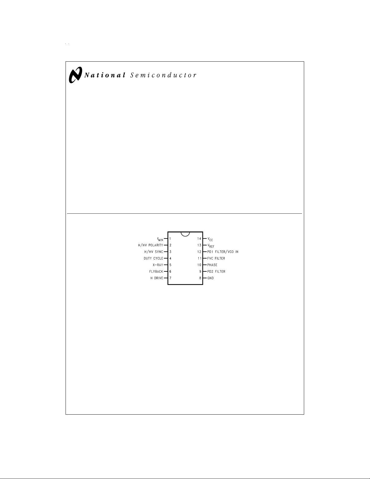
Connection Diagram
FIGURE 1.
Order Number LM1290N
See NS Package Number N14A
Features
n Full autosync—22 kHz to 110 kHz with no component
switching or external adjustments
n No manufacturing trims needed—internal VCO
capacitor trimmed on chip
n Sample-and-hold circuit for fast top-of-screen phase
recovery, even when using composite sync
n DC-controlled H phase and duty cycle
n Resistor-programmable minimum VCO frequency
n Excellent jitter performance
n X-ray input disables H drive until V
n Low V
n H output transistor protected against accidental turn on
during flyback
n Capacitor-programmable frequency ramping, d
protects H output transistor during scanning mode
changes
disables H drive (V
CC
DS012917-1
CC
powered down
CC
<
8.5V)
f
VCO
/dt
,
© 1999 National Semiconductor Corporation DS012917 www.national.com
Page 2
Absolute Maximum Ratings (Notes 1, 3)
If Military/Aerospace specified devices are required,
please contact the National Semiconductor Sales Office/
Distributors for availability and specifications.
Supply Voltage (V
Input Voltage (V
Pin 1 8V
Pins 3, 4, 5, 6 V
Pin 10 1.0V<V
Pin 12 10V
Output Sink Current, Pin 7 130 mA
Power Dissipation (P
(Above 25˚C, derate based on θ
and TJ) 1.65W
) 15V
CC
)
DC
)
D
JA
CC
<
7.5V
DC
Thermal Resistance (θ
Junction Temperature (T
) 75˚C/W
JA
) 150˚C
J
ESD Susceptibility (Note 5) 3.5 kV
Storage Temperature −65˚C to +150˚C
Lead Temperature
(Soldering 10 seconds) 265˚C
Operating Ratings (Note 2)
Operating Temperature Range −20˚C to +80˚C
Supply Voltage 10.8V ≤ V
CC
≤ 13.2V
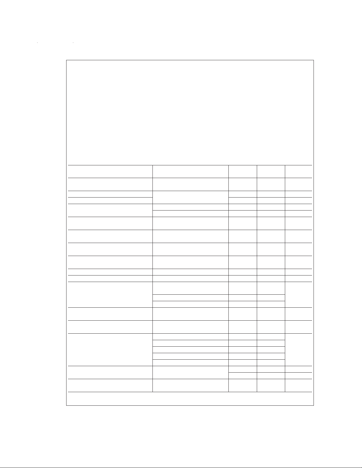
Electrical Characteristics
See Test Circuit (
Figure 2
);T
A
=
25˚C; V
Parameter Condition Typical Limit Units
Supply Current (Pin 14) Pin 3 and Pin 7 Open Circuit, 30 40 mA (max)
Minimum Capture Frequency H Sync Duty Cycle=10%; 10 22 kHz (max)
Maximum Capture Frequency Pin 1 (f
H/HV SYNC Input (Pin 3) High Level 2.2 V (min)
Threshold Voltage Low Level 0.8 V (max)
H/HV SYNC Input (Pin 3) 26 24
Maximum Sync Tip Duty Cycle
H/HV SYNC Input (Pin 3) f
Minimum Sync Tip Duty Cycle
H/HV POLARITY (Pin 2) C
Low Level Output Voltage, V
OL
H/HV POLARITY (Pin 2) C
High Level Output Voltage, V
OH
FVC Gain 22 kHz ≤ fH≤ 110 kHz 0.055 V/kHz
VCO Gain 22 kHz ≤ f
Phase Detector 1 Gain H Sync Duty Cycle=10%:
Phase Detector 1 Output Impedance 20 kΩ
(Pin 12)
Phase Detector 1 Leakage Current + H/HV SYNC Input Grounded 0.3 2 µA
VCO Bias Current (Pin 12)
Jitter f
Free Run Frequency Variation I
H Drive Phase Control Gain V
=
CC
12V; V
=
0V unless otherwise stated.
5
(Note 6) (Note 7)
Pin 1=−100 µA
) Open 115 110 kHz (min)
MIN
=
22 kHz 5
H
=
0.1 µF; I
POL
=
0.1 µF; I
POL
=
f
110 kHz 120
H
=
f
60 kHz 80
H
=
f
22 kHz 30
H
=
110 kHz (Note 8) 0.9
H
=
90 kHz 1.1
f
H
=
f
60 kHz 1.6
H
=
f
31 kHz 3.6
H
=
f
22 kHz 5.8
H
=
−225 µA 32 34 kHz (max)
1
=
+1 µA 0.05 0.4 V (max)
OL
=
−1 µA 4.5 4 V (min)
OL
≤ 110 kHz 18.2 kHz/V
VCO
26 25 kHz (min)
=
2V to 6V (Note 11) 8.89
10
(32) (˚/V)
%
%
µA/radian
ns p-p
%
/V
T
H
www.national.com 2
Page 3
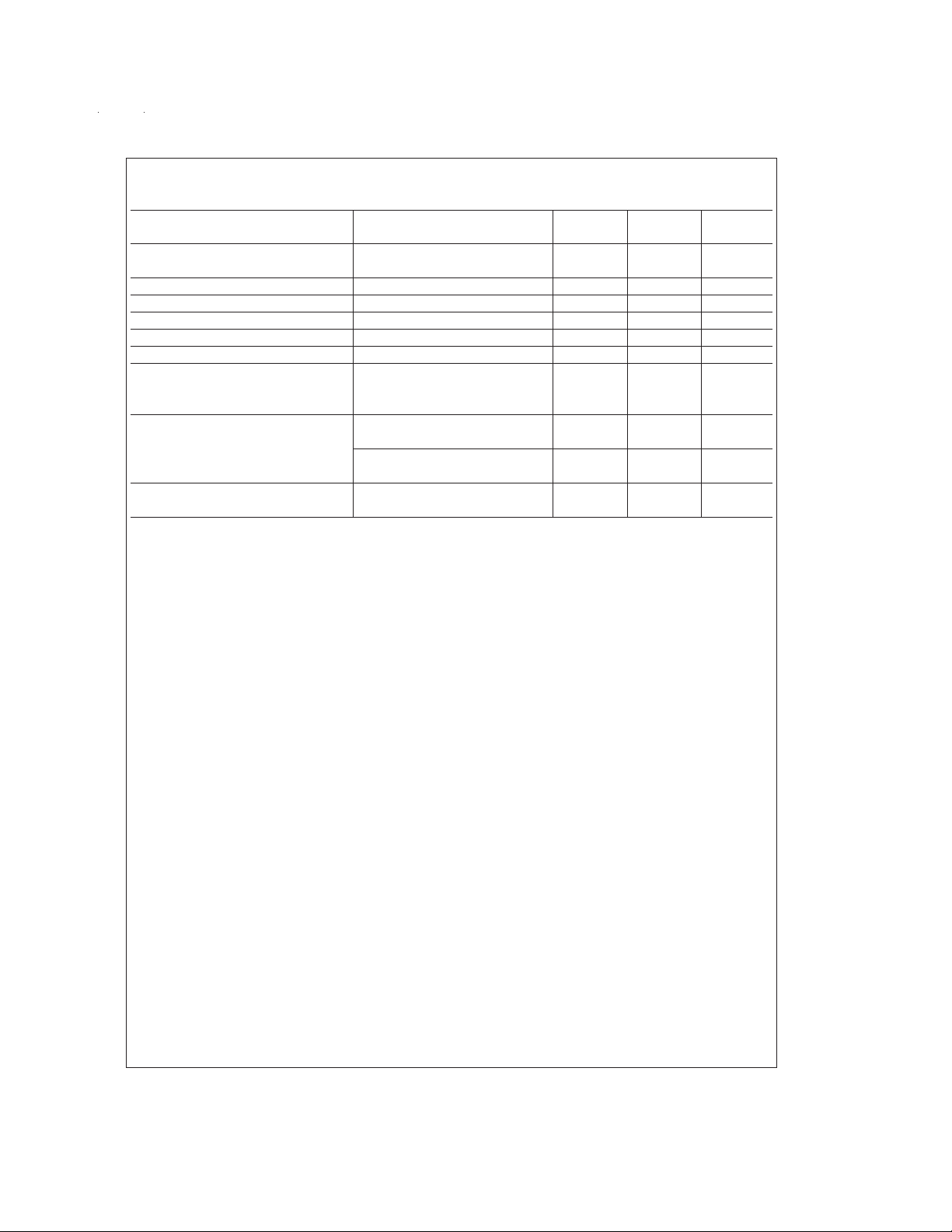
Electrical Characteristics (Continued)
See Test Circuit (
Figure 2
);T
A
=
25˚C; V
Parameter Condition Typical Limit Units
H Drive Phase Control Range V
H Drive Duty Cycle Control Gain V
H Drive Duty Cycle Maximum (Pin 7) V
H Drive Duty Cycle Minimum (Pin 7) V
H Drive Low Level Output Voltage (Pin 7) I
Flyback Input Threshold Voltage (Pin 6) Positive-Going Flyback Pulse 2.2 V
Maximum Allowable Storage Delay of From H Drive Rising Edge to
Horizontal Deflection Output Transistor Center of Flyback Pulse 30
Plus Half of Flyback Pulse Width
V
Lockout Threshold Voltage VCCBelow Threshold: 8.5 V (max)
CC
(Pin 14) H Drive Output Disabled
X-Ray Shutdown Threshold Voltage Above Threshold: 1.85 2 V (min)
(Pin 5) H Drive Output Disabled
Note 1: Absolute Maximum Ratings indicate limits beyond which damage to the device may occur.
Note 2: Operating Ratings indicate conditions for which the device is functional, but do not guarantee specific performance limits. For guaranteed specifications and
test conditions, see the Electrical Characteristics. The guaranteed specifications apply only for the test conditions listed. Some performance characteristics may degrade when the device is not operated under the listed test conditions.
Note 3: All voltages are measured with respect to GND, unless otherwise specified.
Note 4: The maximum power dissipation must be derated at elevated temperatures and is dictated by T
allowable power dissipation at any elevated temperature is P
this device, T
Note 5: Human Body model, 100 pF capacitor discharged through a 1.5 kΩ resistor.
Note 6: Typical specifications are at T
Note 7: Tested limits are guaranteed to National’s AOQL (Average Outgoing Quality Level).
Note 8: The standard deviation, σ, of the flyback pulse period is measured with a HP 53310A Modulation Domain Analyzer.Peak-to-peak jitter of the flyback pulse
is defined by 6σ.
Note 9: A positive phase value represents a phase lead of the flyback pulse peak with reference to the center of H sync.
Note 10: The duty cycle is measured under the conditions of free run with I
and the turn off delay of the H deflection output transistor respectively.
Note 11: T
=
150˚C. The typical thermal resistance (θ
JMAX
=
25˚C and represent most likely parametric norm.
A
is defined as the total time of one horizontal line.
H
=
CC
12V; V
=
0V unless otherwise stated.
5
(Note 6) (Note 7)
=
3.6V to 7V (Notes 9, 11)
10
±
14
(See Application Hint#3)
=
0V to 4V (Note 10) 10.8
4
=
0V (Note 10) 68 63
4
=
4V (Note 10) 25 35
4
=
100 mA 0.7 V
OL
V
Above Threshold: 10.5 V (min)
CC
H Drive Output Enabled
, θJAand the ambient temperature, TA. The maximum
=
3 µs and T
JMAX
=
d
3.5 µs where T
and Tdare the flyback pulse width
FBP
=
(T
D
) of the LM1290N is 75˚C/W.
JA
)/θJAor the number given in the Absolute Maximum Ratings, whichever is lower. For
JMAX−TA
=
−100 µA,T
1
FBP
%
%
%
T
%
/V
(min)
(max)
%
T
H
H
www.national.com3
Page 4

Test Circuit
System Block Diagram
DS012917-2
FIGURE 2.
FIGURE 3.
www.national.com 4
DS012917-3
Page 5

Pin Descriptions
See
Figure 4
through
Figure 10
for input and output sche-
matics.
Pin 1 —f
run frequency of the LM1290. The freerun frequency should
: A resistor from this pin to ground sets the free
MIN
be set typically as:
=
f
0.85(f
MIN
where f
the application. The resistance required to set this frequency
is the minimum lock frequency required for
MINLOCK
MINLOCK
)−2kHz
is approximately:
For example, to find R
31.469 kHz,
=
f
0.85(31.469 kHz)−2kHz=24749
MIN
Rounding to the closest standard 1%resistor gives R
21.5 kΩ.
for VGA which has f
MIN
MINLOCK
MIN
Pin 2—H/HV POLARITY: A 0.1 µF capacitor is connected
from this pin togroundfor detecting the polarity of H/HV sync
at pin 3. A low logic level at pin 2 indicates active-high H/HV
sync to pin 3, a high level indicates active-low. See
Figure 4
for the output schematic.
Pin 3— H/HV SYNC: This input pin accepts DC-coupled H
or composite sync of either polarity. For best noise immunity,
a resistor of 2 kΩ or less should be connected from this pin
to pin 8 (GND) via a short path. See
Figure 5
for the input
schematic.
Pin 4— DUTY CYCLE: A DC voltage applied to this pin sets
the duty cycle of the H DRIVE output (pin 7), with a range of
approximately 30%to 70%. 2V sets the duty cycle to approximately 50%. See
Figure 6
for the input schematic.
Pin 5— X-RAY: This pin is for monitoring CRT anode voltage. If the input voltage exceeds an internal threshold, H
Input/Output Schematics
DRIVE output (pin 7) is latched high. V
to below approximately 2V to clear thelatched condition, i.e.,
power must be turned off. See
CC
Figure 7
matic.
Pin 6 —FLYBACK: Input pin for phase detector 2. For best
operation, the flyback peak should be at least 5V but not
greater than V
ceptable. See
. Any pulse width greater than 1.5 µs is ac-
CC
Figure 8
for the input schematic.
Pin 7 — H DRIVE: This is an open-collector output which
provides the drive pulse for the high power deflection circuit.
The pulse duty cycle is controlled by pin 4. Polarity convention: Horizontal deflection output transistor is on when H
DRIVE OUT is low. See
Figure 9
for the output schematic.
Pin 8— GND: System ground. For best jitter performance,
all bypass capacitors should be connected to this pin via
=
short paths.
Pin 9— PD2 FILTER: The low-pass filter cap of between
0.01 µF to 1 µF for the output of phase detector 2 is connected from this pin to pin 8 (GND) via a short path. A
smaller value increases the response.
Pin 10— PHASE: A DC control voltage applied to this pin
=
sets the phase of the flyback pulse with respect to thecenter
of H sync. See
Figure 10
for the input schematic.
Pin 11— FVC FILTER: A 1 µF capacitor is connected from
this pin to pin 8 (GND) via a short path.
Pin 12 — PD1 OUT/VCO IN: Phase detector 1 has a gated
charge pump output which requires an external low-pass filter. For best jitter performance, the filter should be grounded
to pin 8 (GND) via a short path. Ifa voltagesource is applied
to this pin, the phase detector is disabled and the VCO can
be controlled directly.
Pin 13— V
8.2V reference. It should be decoupled to pin 8 (GND) via a
: This is the decoupling pin for the internal
REF
short path with a cap of at least 470 µF. Do not load this pin.
Pin 14 —V
should be decoupled to pin 8 (GND) via a short path with a
: 12V nominal power supply pin. This pin
CC
cap of at least 47 µF.
has to be reduced
for the input sche-
FIGURE 4.
DS012917-4
DS012917-5
FIGURE 5.
www.national.com5
Page 6

Input/Output Schematics (Continued)
DS012917-7
FIGURE 7.
DS012917-6
FIGURE 6.
DS012917-9
FIGURE 9.
DS012917-8
FIGURE 8.
www.national.com 6
DS012917-10
FIGURE 10.
Page 7

Application Hints
1. Phase Control for Geometry Correction: Pin 10
(PHASE) is designed to control static phase (picture
horizontal position) as well as dynamic phase for geometry correction. Complete control of static and dynamic
phase can be achieved by superposing a correction
waveform (Sawtooth and/or parabola) onthe DC control
voltage at pin 10 (see
2. Programmable Frequency Ramping: H frequency
transitions from high to low present aspecial problem for
deflection output stages without current limiting. If, during such a transition, the output transistor on-time increases excessively before the B+ voltage has decreased to its final level, then the deflection inductor
current ramps too high and the induced flyback pulse
can exceed the breakdownvoltage, BV
transistor.To prevent this, the rate of change of the VCO
frequency must be limited.
Figure 12
).
, of the output
CEX
Recommended Phase Voltage for 640 x 480
Consider a scanning mode transitionat t=0 from f
The VCO frequency as a function of time, f
scribed by the equation,
f
(t)≅f
+(
f
−
f
VCO
1
where τ=40x10
) (1 – exp (−t/τ)),
2
1
3
xC
FVC
.
VCO
to f2.
1
(t), is de-
The above equation can be used to predict VCO behavior during frequency transitions, but in practice the value
of C
is most easily determined empirically. In general,
FVC
large values minimize the chance of exceeding BV
but generate long PLL capture times.
CEX
3. Phase Voltage Range vs Delay Time: The recommended phase voltage range to use on pin 10 (PHASE)
depends on the delay time of the deflection output stage.
Delay time is defined as the time from the rising edge of
H Drive to the center of flyback. For best performance
the phase voltage range should be inthe unshadedarea
of
Figure 11
.
@
60 Hz
,
FIGURE 11.
DS012917-11
www.national.com7
Page 8

Typical Application
*Actual value depends on the application and the ambient noise level inside the monitor.
FIGURE 12.
DS012917-12
www.national.com 8
Page 9

Physical Dimensions inches (millimeters) unless otherwise noted
Order Number LM1290N
NS Package Number N14A
LM1290 Autosync Horizontal Deflection Processor
LIFE SUPPORT POLICY
NATIONAL’S PRODUCTS ARE NOT AUTHORIZED FOR USE AS CRITICAL COMPONENTS IN LIFE SUPPORT
DEVICES OR SYSTEMS WITHOUT THE EXPRESS WRITTEN APPROVAL OF THE PRESIDENT AND GENERAL
COUNSEL OF NATIONAL SEMICONDUCTOR CORPORATION. As used herein:
1. Life support devices or systems are devices or
systems which, (a) are intended for surgical implant
into the body, or (b) support or sustain life, and
whose failure to perform when properly used in
accordance with instructions for use provided in the
2. A critical component is any component of a life
support device or system whose failure to perform
can be reasonably expected to cause the failure of
the life support device or system, or to affect its
safety or effectiveness.
labeling, can be reasonably expected to result in a
significant injury to the user.
National Semiconductor
Corporation
Americas
Tel: 1-800-272-9959
Fax: 1-800-737-7018
Email: support@nsc.com
www.national.com
National does not assume any responsibility for use of any circuitry described, no circuit patent licenses are implied and National reserves the right at any time without notice to change said circuitry and specifications.
National Semiconductor
Europe
Fax: +49 (0) 1 80-530 85 86
Email: europe.support@nsc.com
Deutsch Tel: +49 (0) 1 80-530 85 85
English Tel: +49 (0) 1 80-532 78 32
Français Tel: +49 (0) 1 80-532 93 58
Italiano Tel: +49 (0) 1 80-534 16 80
National Semiconductor
Asia Pacific Customer
Response Group
Tel: 65-2544466
Fax: 65-2504466
Email: sea.support@nsc.com
National Semiconductor
Japan Ltd.
Tel: 81-3-5639-7560
Fax: 81-3-5639-7507
 Loading...