

Page 1
December 2002
LM1247
150 MHz I
2
C Compatible RGB Preamplifier with Internal
512 Character OSD ROM, 512 Character RAM and 4
DACs
2
n I
General Description
The LM1247 pre-amp is an integrated CMOS CRT preamp.
It has an I
the parameters necessary to directly setup and adjust the
gain and contrast in the CRT display. Brightness and bias
can be controlled through the DAC outputs which are well
matched to the LM2479 and LM2480 integrated bias clamp
ICs. The LM1247 preamp is also designed to be compatible
with the LM246x high gain driver family.
Black level clamping of the video signal is carried out directly
on the AC coupled input signal into the high impedance
preamplifier input, thus eliminating the need for additional
clamp capacitors. Horizontal and vertical blanking of the
outputs is provided. Vertical blanking is optional and its
duration is register programmable.
The IC is packaged in an industry standard 24 lead DIP
molded plastic package.
2
C compatible interface which allows control of all
C compatible microcontroller interface
n OSD override allows OSD messages to override video
and the use of burn-in screens with no video input
n 4 DAC outputs (8-bit resolution) for bus controlled CRT
bias and brightness
n Spot killer which blanks the video outputs when V
falls below the specified threshold
n Suitable for use with discrete or integrated clamp, with
software configurable brightness mixer
n Horizontal blanking and OSD synchronization directly
from deflection signals. The blanking can be disabled, if
desired
n Vertical blanking and OSD synchronization directly from
deflection signals. The blanking width is register
programmable and can be disabled, if desired
n Power Saving Mode with 65% power reduction
n Matched to LM246x driver and LM2479/80 bias IC’s
Character RAM and 4 DACs
LM1247 150 MHz I
2
C Compatible RGB Preamplifier with Internal 512 Character OSD ROM, 512
CC
Features
n Internal 512 character OSD ROM usable as either (a)
384 2-color plus 128 4-color characters, (b) 640 2-color
characters, or (c) some combination in between
n Internal 512 character RAM, which can be displayed as
one single or two independent windows
Internal Block Diagram
Applications
n Low end 15" and 17" bus controlled monitors with OSD
n 1024x768 displays up to 85 Hz requiring OSD capability
n Very low cost systems with LM246x driver
20048401
FIGURE 1. Order Number LM1247AAG/NA
See NS Package Number N24D
© 2002 National Semiconductor Corporation DS200484 www.national.com
Page 2

Absolute Maximum Ratings (Notes 1, 3)
If Military/Aerospace specified devices are required, please contact the National Semiconductor Sales Office/
LM1247
Distributors for availability and specifications.
Supply Voltage V
, Pins 10 and 18 6.0V
CC
Peak Video DC Output Source Current
(Any One Amp) Pins 19, 20 or 21 1.5 mA
Voltage at Any Input Pin (V
Video Inputs (pk-pk) 0.0 ≤ V
Thermal Resistance to Ambient (θ
Power Dissipation (P
)VCC+0.5 ≥ VIN≥ −0.5V
IN
) 51˚C/W
JA
)
D
IN
(Above 25˚C Derate Based
and TJ) 2.4W
on θ
JA
Thermal Resistance to case (θ
Junction Temperature (T
J
) 32˚C/W
JC
) 150˚C
≤ 1.2V
ESD Susceptibility (Note 4) 3.0 kV
ESD Machine Model (Note 13) 350V
Storage Temperature −65˚C to +150˚C
Lead Temperature (Soldering, 10 sec.) 265˚C
Operating Ratings (Note 2)
Temperature Range 0˚C to +70˚C
Supply Voltage V
CC
Video Inputs (pk-pk) 0.0V ≤ V
4.75V ≤ VCC≤ 5.25V
≤ 1.0V
IN
Video Signal Electrical Characteristics
Unless otherwise noted: TA= 25˚C, VCC= +5.0V, VIN= 0.70 V
P-P,VABL=VCC,CL
numbers refer to the definitions in Table 1. See (Note 7) for Min and Max parameters and (Note 6) for Typicals.
Symbol Parameter Conditions Min Typ Max Units
I
S
Supply Current Test Setting 1, both supplies, no
output loading. See (Note 8).
I
S-PS
V
O BLK
V
O BLK STEP
Supply Current, Power Save
Mode
Active Video Black Level Output
Voltage
Active Video Black Level Step
Test Setting 1, both supplies, no
output loading. See (Note 8).
Test Setting 4, no AC input signal, DC
offset (register 0x8438 set to 0xd5).
Test Setting 4, no AC input signal.
Size
Max Maximum Video Output Voltage Test Setting 3, Video in = 0.70 V
V
O
LE Linearity Error Test Setting 4, staircase input signal
(see (Note 9)).
t
r
Video Rise Time (Note 5), 10% to 90%, Test Setting 4,
AC input signal.
OS
R
Rising Edge Overshoot (Note 5), Test Setting 4, AC input
signal.
t
f
Video Fall Time (Note 5), 90% to 10%, Test Setting 4,
AC input signal.
OS
F
Falling Edge Overshoot (Note 5), Test Setting 4, AC input
signal.
BW Channel bandwidth (−3 dB) (Note 5), Test Setting 4, AC input
signal.
10 kHz Video Amplifier 10 kHz Isolation (Note 14), Test Setting 8. −60 dB
V
SEP
V
10 MHz Video Amplifier 10 MHz Isolation (Note 14), Test Setting 8. −50 dB
SEP
A
Max Maximum Voltage Gain Test Setting 8, AC input signal. 3.8 4.1 V/V
V
A
C-50% Contrast Attenuation@50% Test Setting 5, AC input signal. −5.2 dB
V
A
Min/AVMax Maximum Contrast Attenuation
V
Test Setting 2, AC input signal.
(dB)
AVG-50% Gain Attenuation@50% Test Setting 6, AC input signal. −4.0 dB
A
G-Min Maximum Gain Attenuation Test Setting 7, AC input signal. −11 dB
V
A
Match Maximum Gain Match between
V
Test Setting 3, AC input signal.
channels
Track Gain Change between channels Tracking when changing from Test
A
V
Setting 8 to Test Setting 5. See (Note
11).
= 8 pF, Video Outputs = 2.0 V
195 250 mA
55 85 mA
1.2 VDC
100 mVDC
P-P
4.0 4.3 V
5%
3.1 ns
2%
2.9 ns
2%
150 MHz
−20 dB
±
0.5
±
0.5 dB
. Setting
P-P
dB
www.national.com 2
Page 3

Video Signal Electrical Characteristics (Continued)
Unless otherwise noted: TA= 25˚C, VCC= +5.0V, VIN= 0.70 V
P-P,VABL=VCC,CL
numbers refer to the definitions in Table 1. See (Note 7) for Min and Max parameters and (Note 6) for Typicals.
Symbol Parameter Conditions Min Typ Max Units
TH ABL Control Range upper limit (Note 12), Test Setting 4, AC input
V
ABL
signal.
Range ABL Gain Reduction Range (Note 12), Test Setting 4, AC input
V
ABL
signal.
A
V 3.5/AV Max
A
V 2.0/AV Max
I
Active ABL Input bias current during
ABL
I
Max ABL input current sink capability (Note 12), Test Setting 4, AC input
ABL
ABL Gain Reduction at 3.5V (Note 12), Test Setting 4, AC input
signal. V
ABL
= 3.5V
ABL Gain Reduction at 2.0V (Note 12), Test Setting 4, AC input
signal. V
ABL
= 2.0V
(Note 12), Test Setting 4, AC input
ABL
signal. V
ABL=VABL
MIN GAIN
signal.
V
Max Maximum ABL Input voltage
ABL
during clamping
ABL Track ABL Gain Tracking Error (Note 9), Test Setting 4, 0.7 V
A
V
(Note 12), Test Setting 4, AC input
signal. I
ABL=IABL
MAX
input signal, ABL voltage set to 4.5V
and 2.5V.
R
IP
Minimum Input resistance (pins 5,
Test Setting 4.
6, 7)
= 8 pF, Video Outputs = 2.0 V
4.8 V
2.8 V
−2 dB
−12 dB
P-P
20 MΩ
P-P
10 µA
1.0 mA
V
CC
0.1
4.5 %
. Setting
+
LM1247
V
OSD Electrical Characteristics
Unless otherwise noted: TA= 25˚C, VCC= +5.0V. See (Note 7) for Min and Max parameters and (Note 6) for Typicals.
Symbol Parameter Conditions Min Typ Max Units
V
OSDHIGH
V
OSDHIGH
V
OSDHIGH
V
OSDHIGH
∆V
∆V
max Maximum OSD Level with OSD
Contrast 11
10 Maximum OSD Level with OSD
Contrast 10
01 Maximum OSD Level with OSD
Contrast 01
00 Maximum OSD Level with OSD
Contrast 00
(Black) Difference between OSD Black
OSD
Level and Video Black Level (same
channel)
(White) Output Match between Channels Palette Set at 111, OSD Contrast =
OSD
Palette Set at 111, OSD Contrast =
11, Test Setting 3
Palette Set at 111, OSD Contrast =
10, Test Setting 3
Palette Set at 111, OSD Contrast =
01, Test Setting 3
Palette Set at 111, OSD Contrast =
00, Test Setting 3
Register 08=0x18, Input Video =
Black, Same Channel, Test Setting
8
11, Maximum difference between R,
4.5 V
3.9 V
3.2 V
2.4 V
20 mV
3%
G and B
V
(Track) Output Variation between Channels OSD contrast varied from max to
OSD-out
min
3%
DAC Output Electrical Characteristics
Unless otherwise noted: TA= 25˚C, VCC= +5.0V, VIN= 0.7V, V
ABL=VCC,CL
for Min and Max parameters and (Note 6) for Typicals. DAC parameters apply to all 4 DACs.
Symbol Parameter Conditions Min Typ Max Units
V
Min DAC
V
Max DAC
Mode 00
V
Max DAC
Mode 01
Min output voltage of DAC Register Value = 0x00 0.5 0.7 V
Max output voltage of DAC Register Value = 0xFF,
DCF[1:0] = 00b
Max output voltage of DAC in
DCF mode 01
Register Value = 0xFF,
DCF[1:0] = 01b
= 8 pF, Video Outputs = 2.0 V
3.7 4.2 V
1.85 2.35 V
. See (Note 7)
P-P
www.national.com3
Page 4

DAC Output Electrical Characteristics (Continued)
Unless otherwise noted: TA= 25˚C, VCC= +5.0V, VIN= 0.7V, V
LM1247
for Min and Max parameters and (Note 6) for Typicals. DAC parameters apply to all 4 DACs.
ABL=VCC,CL
Symbol Parameter Conditions Min Typ Max Units
∆V
Max DAC
(Temp)
∆V
Max DAC(VCC
Variation in voltage of DAC with
temperature
) DAC output voltage variation with
V
CC
<T<
0
70˚C ambient
VCCvaried from 4.75V to 5.25V, DAC
register set to mid-range (0x7F)
Linearity Linearity of DAC over its range 5 %
Monotonicity Monotonicity of the DAC
Excluding dead zones
I
MAX
Max Load Current −1.0 1.0 mA
= 8 pF, Video Outputs = 2.0 V
±
0.5 mV/˚C
50 mV
±
0.5 LSB
. See (Note 7)
P-P
System Interface Signal Characteristics
Unless otherwise noted: TA= 25˚C, VCC= +5.0V, VIN= 0.7V, V
ABL=VCC,CL
for Min and Max parameters and (Note 6) for Typicals. DAC parameters apply to all 4 DACs.
Symbol Parameter Conditions Min Typ Max Units
V
VTH+
VFLYBACK positive switching
Vertical Blanking triggered
guarantee
V
SPOT
V
Ref
V
(SCL, SDA) Logic Low Input Voltage −0.5 1.5 V
IL
V
(SCL, SDA) Logic High Input Voltage
IH
(SCL, SDA) Logic Low Input Current SDA or SCL, Input Voltage = 0.4V
I
L
I
(SCL, SDA) Logic High Input Voltage SDA or SCL, Input Voltage = 4.5V
H
V
(SCL, SDA) Logic Low Output Voltage IO= 3 mA 0.5 V
OL
f
Min Minimum Horizontal Frequency PLL & OSD Operational; PLL Range
H
Spot Killer Voltage (Note 17), VCCAdjusted to Activate 3.4 3.9 4.3 V
V
Output Voltage (pin 2) 1.25 1.45 1.65 V
Ref
=0
Max Maximum Horizontal Frequency PLL & OSD Operational; PLL Range
f
H
=3
Max Horizontal Flyback Input Current Absolute Maximum During
I
HFB IN
Flyback
I
IN
I
HFB OUT
I
OUT
I
IN THRESHOLD
t
H-BLANK ON
Max Horizontal Flyback Input Current Absolute Maximum During Scan −700 µA
Peak Current during flyback Design Value 4 mA
Peak Current during Scan Not exact - Duty Cycle Dependent −550 µA
IINH-Blank Detection Threshold 0 µA
H-Blank Time Delay - On + Zero crossing of I
output blanking start. I
t
H-BLANK OFF
H-Blank Time Delay - Off − Zero crossing of I
output blanking end. I
V
f
Max Maximum Video Blanking Level Test Setting 4, AC input signal 0 0.25 V
BLANK
FREERUN
Free Run H Frequency, including
H Blank
t
PW CLAMP
V
CLAMP MAX
Minimum Clamp Pulse Width See (Note 15) 200 ns
Maximum Low Level Clamp
Video Clamp Functioning
Pulse Voltage
V
CLAMP MIN
Minimum High Level Clamp
Video Clamp Functioning
Pulse Voltage
Low Clamp Gate Low Input Current V23= 2V −0.4 µA
I
CLAMP
I
High Clamp Gate High Input Current V23= 3V 0.4 µA
CLAMP
t
CLAMP-VIDEO
Time from End of Clamp Pulse to
Start of Video
Referenced to Blue, Red and Green
inputs
= 8 pF, Video Outputs = 2.0 V
to 50% of
HFB
= +1.5mA
24
to 50% of
HFB
= −100µA
24
. See (Note 7)
P-P
2.0 V
3.0
±
±
VCC+
0.5
10 µA
10 µA
25 kHz
110 kHz
5mA
45 ns
85 ns
42 kHz
2.0 V
3.0 V
50 ns
V
www.national.com 4
Page 5

System Interface Signal Characteristics (Continued)
Note 1: Limits of Absolute Maximum Ratings indicate below which damage to the device must not occur.
Note 2: Operating ratings indicate conditions for which the device is functional, but do not guarantee specific performance limits.
Note 3: All voltages are measured with respect to GND, unless otherwise specified.
Note 4: Human body model, 100 pF discharged through a 1.5 kΩ resistor.
<
Note 5: Input from signal generator: t
Note 6: Typical specifications are specified at +25˚C and represent the most likely parametric norm.
Note 7: Datasheet min/max specification limits are guaranteed by design, test, or statistical analysis. The guaranteed specifications apply only for the test conditions
listed. Some performance characteristics may change when the device is not operated under the listed test conditions.
Note 8: The supply current specified is the quiescent current for V
therefore all the supply current is used by the pre-amp.
Note 9: Linearity Error is the maximum variation in step height of a 16 step staircase input signal waveform with a 0.7 V
with each at least 100 ns in duration.
Note 10: dt/dV
Note 11: ∆A
gain change between any two amplifiers with the contrast set to A
amplifiers’ gains might be 12.1 dB, 11.9 dB, and 11.8 dB and change to 2.2 dB, 1.9 dB and 1.7 dB respectively for contrast set to A
gain change of 10.0 dB with a tracking change of
Note 12: The ABL input provides smooth decrease in gain over the operational range of 0 dB to −5 dB: ∆A
V
ABL MIN GAIN
Note 13: Machine Model ESD test is covered by specification EIAJ IC-121-1981. A 200 pF cap is charged to the specific voltage, then discharged directly into the
IC with no external series resistor (resistance of discharge path must be under 50Ω).
Note 14: Measure output levels of the other two undriven amplifiers relative to the driven amplifier to determine channel separation. Terminate the undriven amplifier
inputs to simulate generator loading. Repeat test at f
Note 15: A minimum pulse width of 200 ns is the guaranteed minimum for a horizontal line of 15 kHz. This limit is guaranteed by design. If a lower line rate is used
then a longer clamp pulse may be required.
Note 16: Adjust input frequency from 10 MHz (A
Note 17: Once the spot killer has been activated, the LM1247 remains in the off state until V
= 200*(t
CC
track is a measure of the ability of any two amplifiers to track each other and quantifies the matching of the three gain stages. It is the difference in
V
). Beyond −5 dB the gain characteristics, linearity and pulse response may depart from normal values.
5.5V–t4.5V
r,tf
)/ ((t
1 ns.
and 5V Dig with RL=∞. Load resistors are not required and are not used in the test circuit,
CC
5.5V+t4.5V
)) %/V, where: t
±
0.2 dB.
= 10 MHz for V
IN
max reference level) to the −3 dB corner frequency (f
V
is the rise or fall time at VCC= 5.5V, and t
5.5V
C−50% and measured relative to the AVmax condition. For example, at AVmax the three
V
10 MHz.
SEP
level at the input. All 16 steps equal,
P-P
is the rise or fall time at VCC= 4.5V.
4.5V
C−50%. This yields a typical
V
= A(V
ABL
).
−3 dB
is cycled (reduced below 0.5V and then restored to 5V).
CC
ABL=VABL MAX GAIN
)–A(V
ABL
LM1247
=
Hexadecimal and Binary Notation
Hexadecimal numbers appear frequently throughout this
document, representing slave and register addresses, and
register values. These appear in the format “0x...”. For example, the slave address for writing the registers of the
LM1247 is hexadecimal BA, written as 0xBA. On the other
hand, binary values, where the individual bit values are
shown, are indicated by a trailing “b”. For example, 0xBA is
equal to 10111010b. A subset of bits within a register is
referred to by the bit numbers in brackets following the
TABLE 1. Test Settings
Control No. of Bits
Contrast 7 0x7F
B, R, G
7 0x7F
Gain
DC Offset 3 0x00
1234 5678
(Max)
(Max)
0x00
Min
0x7F
(Max)
0x7F
(Max)
0x7F
(Max)
0x05 0x07
(Min)
(Max)
register value. For example, the OSD contrast bits are the
fourth and fifth bits of register 0x8438. Since the first bit is bit
0, the OSD contrast register is 0x8438[4:3].
Register Test Settings
Table 1 shows the definitions of the Test Settings 1–8 referred to in the specifications sections. Each test setting is a
combination of five hexadecimal register values, Contrast,
Gain (Blue, Red, Green) and DC offset.
Test Settings
0x7F
(Max)
Set V
O
2V
P-P
0x05 0x05 0x05 0x05 0x05
0x40
(50.4%)
to
0x7F
(Max)
0x7F
(Max)
0x40
(50.4%)
0x7F
(Max)
0x00
(Min)
0x7F
(Max)
0x7F
(Max)
www.national.com5
Page 6

LM1253A and LM1237 Compatibility
In order to maintain register compatibility with the LM1253A
LM1247
and LM1237 preamplifier datasheet assignments for bias
and brightness, the color assignments are recommended as
TABLE 2. LM1253A/LM1237 Compatibility
LM1247 Pin: DAC 1 DAC 2 DAC 3 DAC 4
Assignment: Blue Green Red Brightness
shown in Table 2. If datasheet compatibility is not required,
then the DAC assignments can be arbitrary.
DAC Bias Outputs
OSD vs Video Intensity
The OSD amplitude has been increased over the LM1237
level. During monitor alignment, the three gain registers are
used to achieve the desired front of screen color balance.
This also causes the OSD channels to be adjusted accordingly, since these are inserted into the video channels prior
to the gain attenuators. This provides the means to fine tune
the intensity of the OSD relative to the video as follows. If a
typical starting point for the alignment is to have the gains at
maximum (0x7F) and the contrast at 0x55, the resultant
OSD intensity will be higher than if the starting point is with
the gains at 0x55 and the contrast at maximum (0x7F). This
tradeoff allows fine tuning the final OSD intensity relative to
the video. In addition, the OSD contrast register, 0x8438
[4:3], provides 4 major increments of intensity. Together,
these allow setting the OSD intensity to the most pleasing
level.
ESD Protection
The LM1247 features a 3.0 KV ESD protection level (see
(Notes 4, 13)). This is provided by special internal circuitry
which activates when the voltage at any pin goes beyond the
supply rails by a preset amount. At that time the protection is
applied to all pins, including SDA and SCL. If any signal
other than these two is applied to the LM1247 while the V
is near zero, such as horizontal and vertical deflection pulses
of sufficient amplitude, this protection will activate and prevent any communication on the I
LM1247, until the other signal or signals are removed. Normally, with all other pins unenergized, the LM1247 will not
2
C communication when it is powered down.
affect I
2
C bus common to the
CC
www.national.com 6
Page 7
LM1247
Typical Performance Characteristics V
20048402
FIGURE 2. Logic Horizontal Blanking
= 5V, TA= 25˚C unless otherwise specified
CC
FIGURE 5. Deflection Vertical Blanking
20048405
FIGURE 3. Logic Vertical Blanking
FIGURE 4. Deflection Horizonal Blanking
20048403
20048404
20048406
FIGURE 6. Logic Clamp Pulse
20048407
FIGURE 7. Red Cathode Response
www.national.com7
Page 8
Typical Performance Characteristics V
= 5V, TA= 25˚C unless otherwise specified (Continued)
CC
LM1247
20048408
FIGURE 8. ABL Gain Reduction Curve
SYSTEM INTERFACE SIGNALS
The Horizontal and Vertical Blanking and the Clamping input signals are important for proper functionality of the LM1247. Both
blanking inputs must be present for OSD synchronization. In addition, the Horizontal blanking input also assists in setting the
proper cathode black level, along with the Clamping pulse. The Vertical blanking input initiates a blanking level at the LM1247
outputs which is programmable from 3 to 127 lines (we recommend at least 10). Both horizontal and vertical blanking can be
individually disabled, if desired.
Figure 2 and Figure 3 show the case where the Horizontal and Vertical inputs are logic levels. Figure 2 shows the smaller pin 24
voltage superimposed on the horizontal blanking pulse input to the neck board with R
voltage at pin 24 is clamped to about 1 volt when the pin is sinking current. Figure 3 shows the smaller pin 1 voltage
superimposed on the vertical blanking input to the neck board with C
jumpered and RV= 4.7k. These component values
4
correspond to the application circuit of Figure 9.
Figure 4 and Figure 5 show the case where the horizontal and vertical inputs are from deflection. Figure 4 shows the pin 24
voltage which is derived from a horizontal flyback pulse of 35V peak to peak with R
the pin 1 voltage which is derived from a vertical flyback pulse of 55V peak to peak with C
Figure 6 shows the pin 23 clamp input voltage superimposed on the neck board clamp logic input pulse. R
chosen to limit the pin 23 voltage to about 2.5V peak to peak. This corresponds to the application circuit given in Figure 9.
= 4.7k and C17= 0.1 µF. Note where the
H
= 8.2K and C17jumpered. Figure 5 shows
H
= 1500 pF and RV= 120k.
4
= 1k and should be
31
CATHODE RESPONSE
Figure 7 shows the response at the red cathode for the application circuit in Figures 9, 10. The input video risetime is 1.5 ns. The
resulting leading edge has a 7.1 ns risetime and a 7.6% overshoot, while the trailing edge has a 7.1 ns risetime and a 6.9%
overshoot with an LM2467 driver.
ABL GAIN REDUCTION
The ABL function reduces the contrast level of the LM1247 as the voltage on pin 22 is lowered from V
shows the amount of gain reduction as the voltage is lowered from V
(5.0V) to 2V. The gain reduction is small until V22reaches
CC
to around 2V. Figure 8
CC
the knee anound 3.7V, where the slope increases. Many system designs will require about 3 dB to 5 dB of gain reduction in full
beam limiting. Additional attenuation is possible, and can be used in special circumstances. However, in this case, video
performance such as video linearity and tracking between channels will tend to depart from normal specifications.
OSD PHASE LOCKED LOOP
Table 3 shows the recommended horizontal scan rate ranges (in kHz) for each combination of PLL register setting, 0x843E [1:0],
and the pixels per line register setting, 0x8401 [7:5]. These ranges are recommended for chip ambient temperatures of 25
o
C. While the OSD PLL will lock for other register combinations and at scan rates outside these ranges, the performance of the
70
loop will be improved if these recommendations are followed. NR means the combination of PLL and PPL is not recommended
for any scan rate.
www.national.com 8
o
Cto
Page 9
LM1247
Typical Performance Characteristics V
=5V,TA= 25˚C unless otherwise specified (Continued)
CC
TABLE 3. OSD Register recommendations
PPL=0 PPL=1 PPL=2 PPL=3 PPL=4 PPL=5 PPL=6 PPL=7
PLL=1 25 - 61 25 - 53 25 - 48 25 - 43 25 - 40 25 - 36 25 - 34 25 - 31
PLL=2 NR NR 48 - 98 43 - 88 40 - 81 36 - 74 34 - 69 31 - 64
PLL=3 NR NR NR 88 - 110 81 - 110 74 - 110 69 - 110 64 - 110
Pin Descriptions and Application Information
Pin
No.
Pin Name Schematic Description
1 V Flyback
Required for OSD synchronization and is also
used for vertical blanking of the video outputs.
The actual switching threshold is about 35% of
. For logic level inputs C4can be a jumper,
V
CC
but for flyback inputs, an AC coupled
differentiator is recommended, where R
enough to prevent the voltage at pin 1 from
exceeding V
CC
be small enough to flatten the vertical rate ramp
2V
REF
at pin 1. C
Bypass Provides filtering for the internal voltage which
24
sets the internal bias current in conjunction with
. A minimum of 0.1 µF is recommended for
R
EXT
proper filtering. This capacitor should be placed
as close to pin 2 and the pin 4 ground return as
possible.
or going below GND. C4should
may be needed to reduce noise.
is large
V
3V
REF
4 Analog Input
Ground
5
Blue Video In
6
Red Video In
7
Green Video In
External resistor, 10k 1%, sets the internal bias
current level for optimum performance of the
LM1247. This resistor should be placed as close
to pin 3 and the pin 4 ground return as possible.
This is the ground for the input analog portions
of the LM1247 internal circuitry.
These video inputs must be AC coupled with a
.0047 µF cap. Internal DC restoration is done at
these inputs. A series resistor of about 33Ω and
external ESD protection diodes should also be
used for protection from ESD damage.
www.national.com9
Page 10
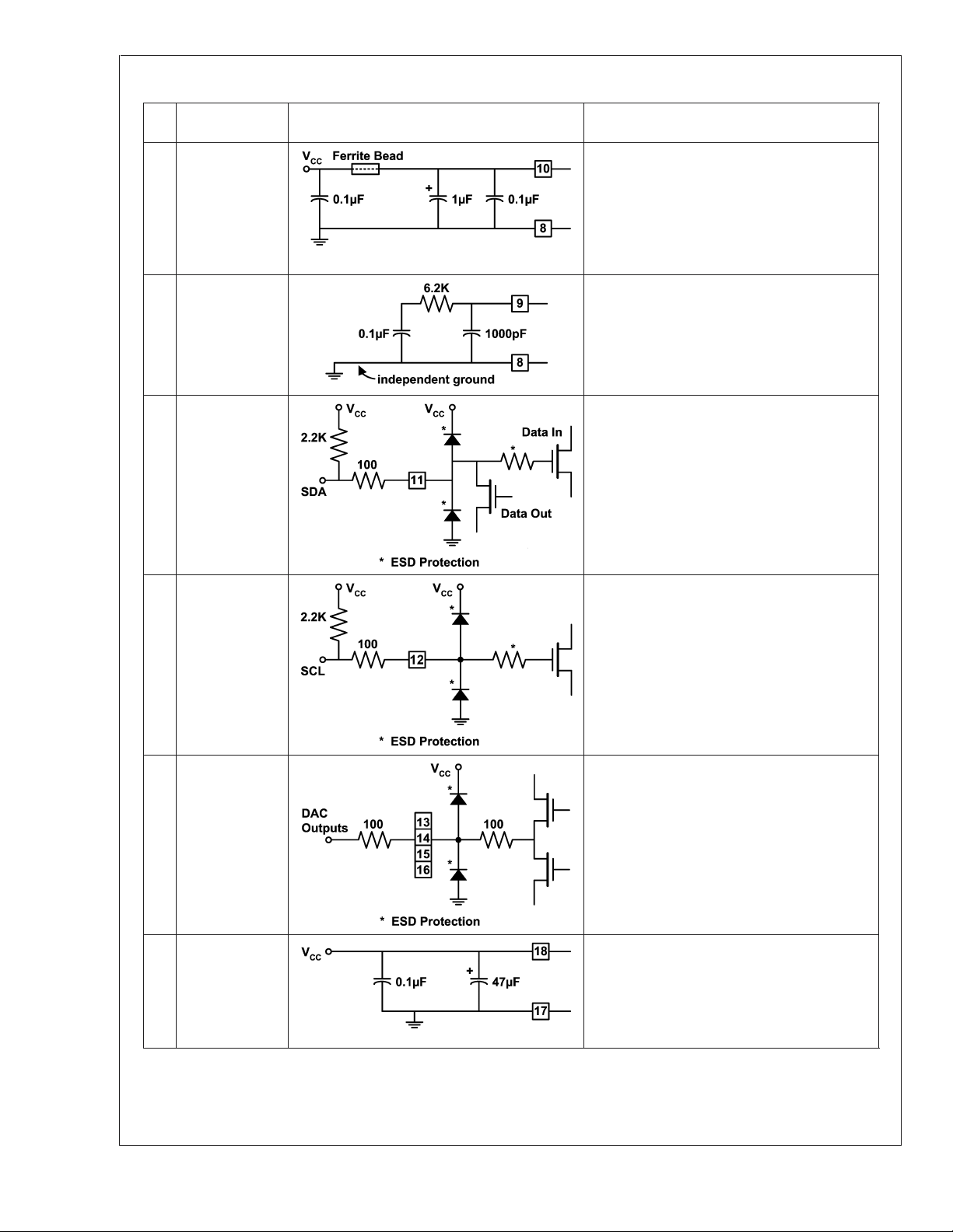
Pin Descriptions and Application Information (Continued)
LM1247
Pin
No.
Pin Name Schematic Description
810Digital Ground
PLL V
CC
9 PLL Filter
The ground pin should be connected to the rest
of the circuit ground by a short but independent
PCB trace to prevent contamination by
extraneous signals. The V
isolated from the rest of the V
pin should be
CC
line by a ferrite
CC
bead and bypassed to pin 8 with an electrolytic
capacitor and a high frequency ceramic.
Recommended topology and values are shown
to the left. It is recommended that both filter
branches be bypassed to the independent
ground as close to pin 8 as possible. Great care
should be taken to prevent external signals from
2
coupling into this filter from video, I
C, etc.
11 SDA
12 SCL
13
DAC 4 Output
14
DAC 2 Output
15
DAC 3 Output
16
DAC 1 Output
The I2C compatible data line. A pull-up resistor
of about 2 kΩ should be connected between this
pin and V
. A resistor of at least 100Ω should
CC
be connected in series with the data line for
additional ESD protection.
The I2C compatible clock line. A pull-up resistor
of about 2 kΩ should be connected between this
pin and V
. A resistor of at least 100Ω should
CC
be connected in series with the clock line for
additional ESD protection.
DAC outputs for cathode cut-off adjustments and
brightness control. DAC 4 can be set to change
the outputs of the other three DACs, acting as a
brightness control. The DAC values and the
2
special DAC 4 function are set through the I
C
compatible bus. A resistor of at least 100Ω
should be connected in series with these outputs
for additional ESD protection.
17
18
www.national.com 10
Ground
V
CC
Ground pin for the output analog portion of the
LM1247 circuitry, and power supply pin for all
the analog of the LM1247. Note the
recommended charge storage and high
frequency capacitors which should be as close
to pins 17 and 18 as possible.
Page 11
Pin Descriptions and Application Information (Continued)
LM1247
Pin
No.
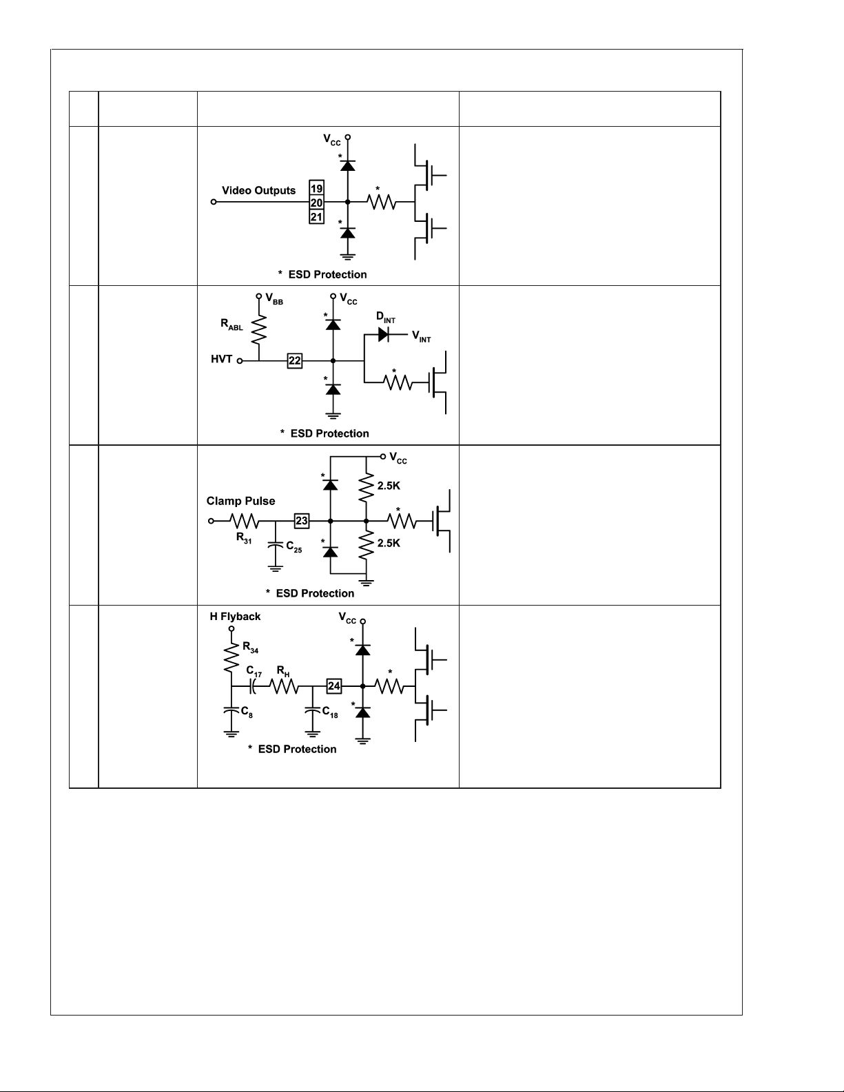
19
20
21
Pin Name Schematic Description
Green Output
Red Output
Blue Output
22 ABL
23 CLAMP
These are the three video output pins. They are
intended to drive the LM246x family of cathode
drivers. Nominally, about 2V peak to peak will
produce 40V peak to peak of cathode drive.
The Automatic Beam Limiter input is biased to
the desired beam current limit by R
and normally keeps D
forward biased. When
INT
ABL
and V
BB
the current resupplying the CRT capacitance
(averaged by C
) exceeds this limit, then D
ABL
INT
begins to turn off and the voltage at pin 22
begins to drop. The LM1247 then lowers the
gain of the three video channels until the beam
current reaches an equilibrium value.
This pin accepts either TTL or CMOS logic
levels. The internal switching threshold is
approximately one-half of V
series resistor, R
, of about 1K is
31
. An external
CC
recommended to avoid overdriving the input
devices. In any event, R
must be large
EXT
enough to prevent the voltage at pin 23 from
going higher than V
or below GND.
CC
24 H Flyback
Proper operation requires current reversal. R
H
should be large enough to limit the peak current
at pin 24 to about +4 ma during blanking, and
−500 µA during scan. C
is usually needed for
17
logic level inputs and should be large enough to
make the time constant, R
larger than the horizontal period. R
HC17
significantly
and C8are
34
typically 300Ω and 330 pF when the flyback
waveform has ringing and needs filtering. C
18
may be needed to filter extraneous noise and
can be up to 100 pF.
www.national.com11
Page 12
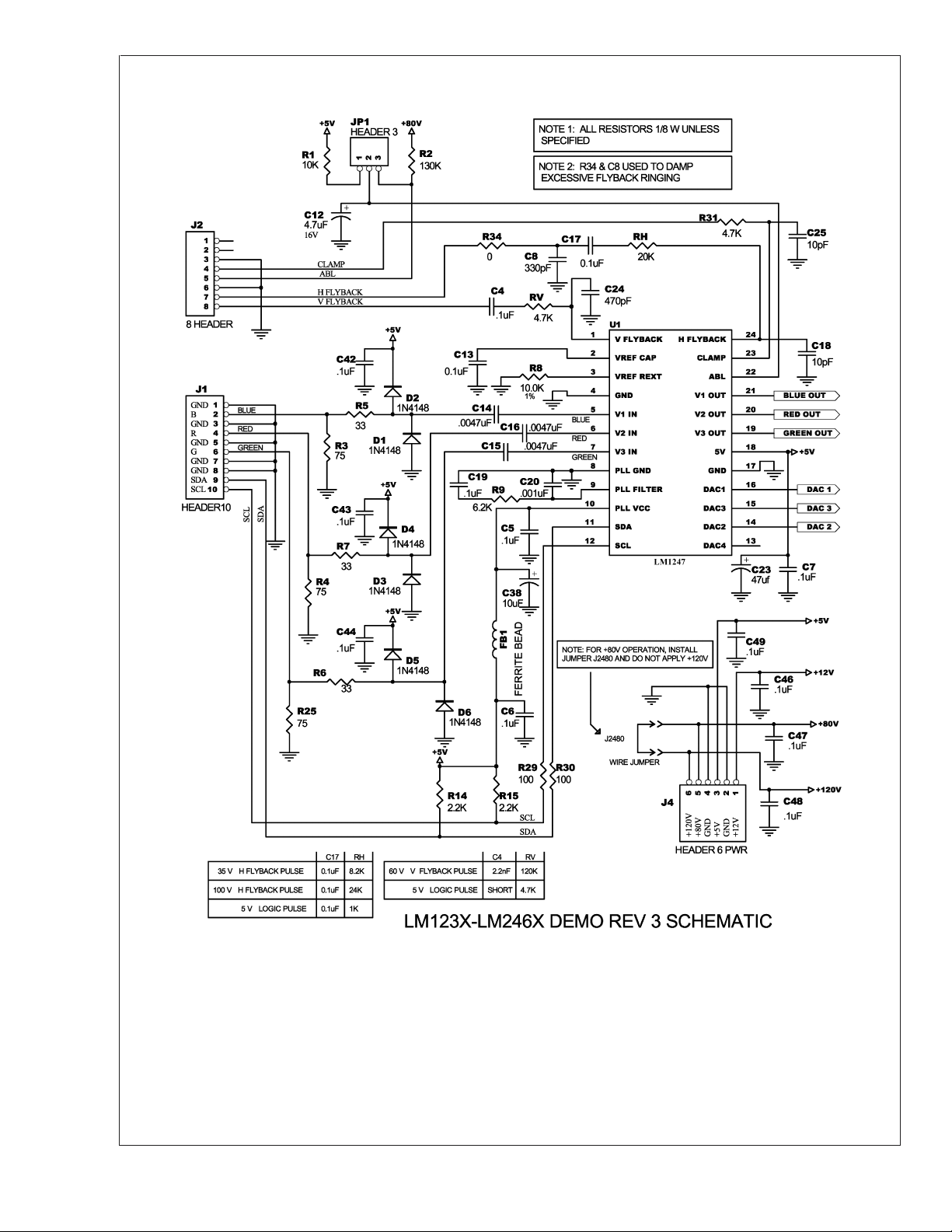
Schematic Diagram
LM1247
FIGURE 9. LM123x/LM124x-LM246x Demo Board Schematic
www.national.com 12
20048424
Page 13
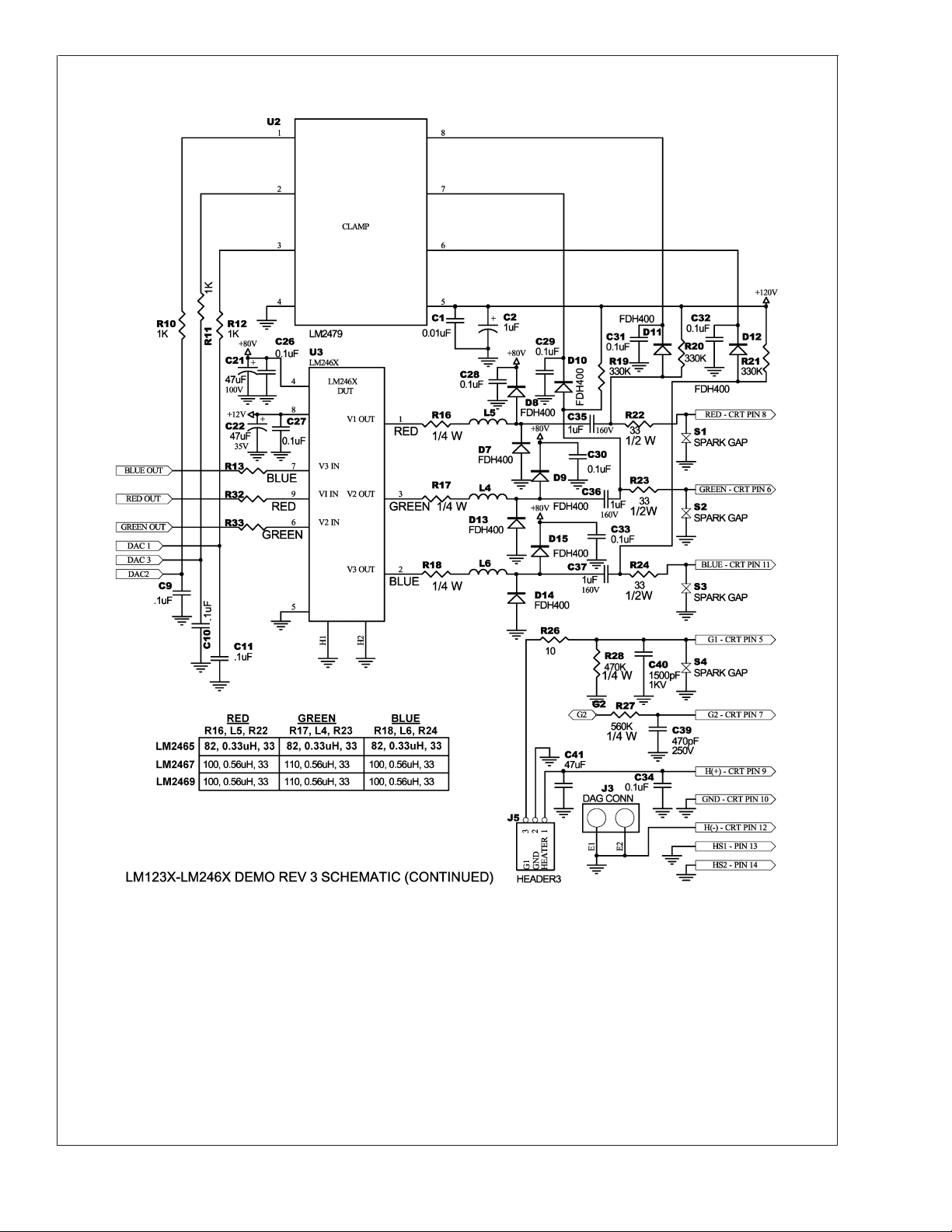
Schematic Diagram
LM1247
FIGURE 10. LM123x/LM124x-LM246x Demo Board Schematic (continued)
20048425
www.national.com13
Page 14
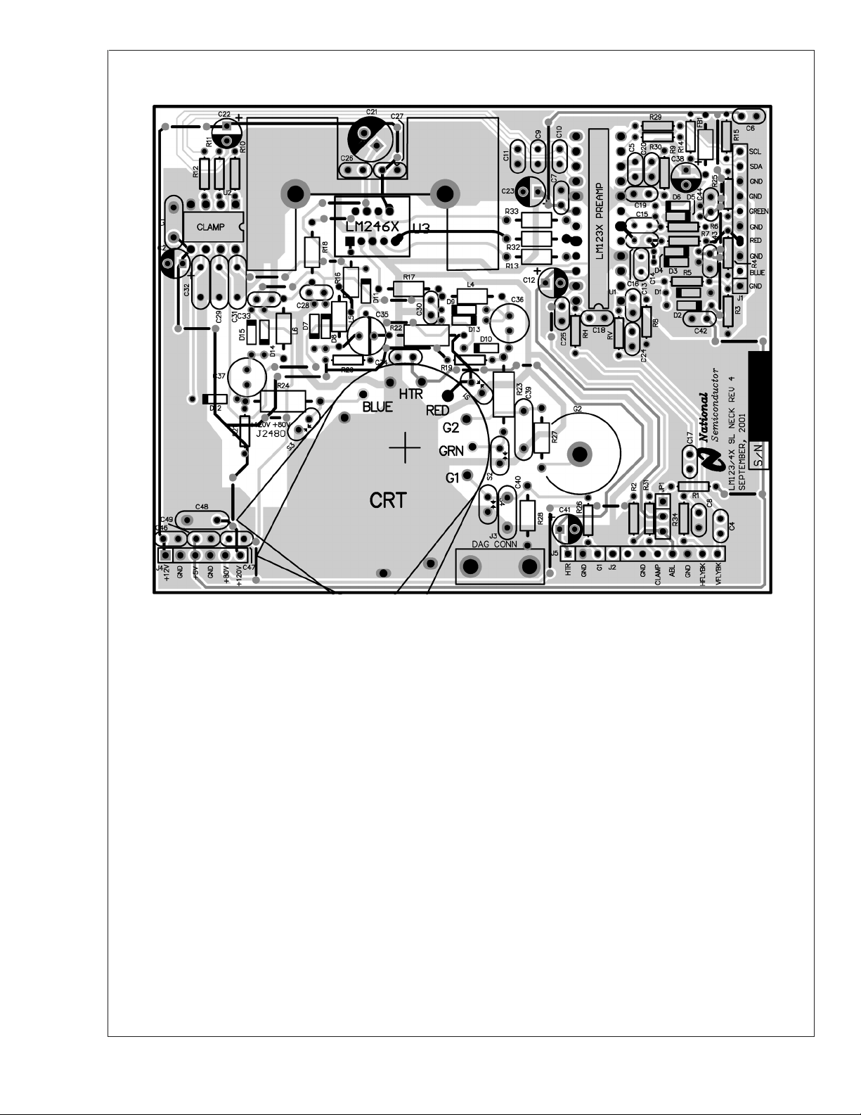
PCB Layout
LM1247
FIGURE 11. LM123x/LM124x-LM246x Demo Board Layout
20048426
www.national.com 14
Page 15
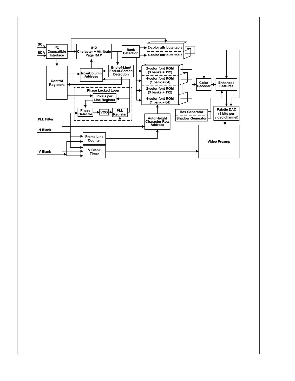
OSD Generator Operation
LM1247
FIGURE 12. OSD Generator Block Diagram
PAGE OPERATION
Figure 12 shows the block diagram of the OSD generator.
OSD screens are created using any of the 512 predefined
characters stored in the mask programmed ROM. The OSD
image is composed of up to 512 characters stored in page
RAM, where each character has a unique 8-bit address. This
means only half of the 512 ROM characters can be displayed at any one time. Since a 9 bit address is needed to
select from 512 ROM addresses, a bank select register is
used to convert the upper 2 bits of the character code into a
3 bit bank address which is combined with the other 6 bits to
produce the necessary 9 bits. Also, since the lower 6 bits can
address 64 characters, this gives a bank size of 64. Therefore, the ROM consists of 8 banks of 64 characters each,
where 4 of these 8 banks are displayed by loading the 4
bank address registers with the appropriate 3 bit code. This
allows the programmer to switch between two different OSD
images, by simply reprogramming the bank addresses.
OSD ROM CONFIGURATION
The OSD ROM is equivalent to two 256 character ROMs of
the type used in the LM1253A and LM1237. Because of the
bank select method described earlier, each can be considered as a group of 3 banks (192) two-color characters followed by 1 bank (64) four-color characters. Physically, the
combined ROM is then 192x2 + 64x4 + 192x2 + 64x4. This
is shown in Figure 12.
BANK ADDRESSING
A pictorial view of this addressing method is shown in Figure
13. On the left side is a section of the Page RAM with four
different addresses in successive locations, which have
been chosen to demonstrate accessing 4 of the 8 ROM
banks using the Bank Select Registers. The first has 10b for
20048427
the two most significant bits, so the OSD generator looks in
B2AD[2:0], located in Bank Select Register B, for its ROM
bank address. SInce B2AD[2:0] contains 101b, the character
font is read from Bank 5. The complete font address is
composed of this bank address, plus the lower six bits of the
original byte in Page RAM, giving a ROM address of
101101110b. The remaining addresses demonstrate that the
four selected banks can be displayed in any order.
END-OF-LINE AND END-OF-SCREEN CODES
There are two special character addresses used in the page
RAM, 0x00 (End-of-Screen) and 0x01 (End-of-Line). The
first must be used to terminate a window and the second to
terminate a line. The LM1247 is different from the LM1253A
and LM1237 in that these are now not actually encoded into
ROM, but are instead detected by the logic as the OSD
image is read from page RAM. This means that the two
lowest locations in the bank which is currently selected by
Bank Select Register 0, 0x8427[2:0], cannot be displayed in
an OSD image. However, these two characters can be
masked in the ROM, and if this bank is selected by Bank
Select Registers 1, 2 or 3, then these two characters are
usable on screen. The consequences of this is that only 254
ROM characters are displayable at one time.
DISPLAYING AN OSD IMAGE
Consecutive lines of characters make up the displayed window. These characters are stored in the page RAM through
2
C compatible bus. Each line can contain any number of
the I
characters up to the limit of the displayable line length (dependent on the pixels per line register), although some restrictions concerning the enhanced features apply on character lines longer than 32 characters. The number of
characters across the width and height of the page can be
www.national.com15
Page 16

OSD Generator Operation (Continued)
varied under I
LM1247
characters that can be stored and displayed on the screen is
2
C compatible control, but the total number of
limited to 512 including any End-of-Line and End-of-Screen
characters. The horizontal and vertical start position can also
be programmed through the I
2
C compatible bus.
FIGURE 13. Bank Addressing
WINDOWS
Two separate windows can be opened, utilizing the data
stored in the page RAM. Each window has its own horizontal
and vertical start position, although the second window
should be horizontally spaced at least two character spaces
away from the first window, and should never overlap the
first window when both windows are on. The OSD window
must be placed within the active video.
OSD VIDEO DAC
The OSD DAC is controlled by the 9-bit (3x3 bits) OSD video
information coming from the pixel serializer look-up table.
The look-up table in the OSD palette is programmed to
20048428
select 4 color levels out of 8 linearly spaced levels per
channel. The OSD DAC is shown in Figure 14, where the
gain is programmable by the 2-bit OSD contrast register, in 4
stages to give the required OSD signal. The OSD DACs use
the reference voltage, V
, to bias the OSD outputs.
REF
OSD VIDEO TIMING
The OSD analog signal then goes to the switch, shown in
Figure 14 and Figure 1 where the timing control switches
from input video to OSD and back again as determined by
the control registers. This is also where horizontal and vertical blanking are also inserted at their appropriate intervals.
www.national.com 16
Page 17

OSD Generator Operation (Continued)
FIGURE 14. Block Diagram of OSD DACs
LM1247
20048429
CHARACTER CELL
Each character is defined as a 12 column by 18 row matrix of
picture elements, or “pixels”. The character font is shown in
Figure 29 through Figure 36. There are two types of characters defined in the character ROM:
1. Two-color: There are a total of 384 two-color characters
in 6 banks (banks 0, 1, 2, 4, 5 and 6). Each pixel of these
characters is defined by a single bit value. If the bit value
is 0, then the color is defined as “Color 0” or the “background” color. If the bit value is 1, then the color is
defined as “Color 1”, or the “foreground” color. An example of a character is shown in Figure 15. The grid
lines are shown for clarity to delineate individual pixels
and are not part of the actual displayed character.
2. Four-color: There are a total of 128 four-color characters, in two banks of 64 (banks 3 and 7). Each pixel of
the four-color character is defined by two bits of information, and thus can define four different colors, Color
0, Color 1, Color 2 and Color 3. Color 0 is defined as the
“background” color. All other colors are considered “fore-
ground” colors, although for most purposes, any of the
four colors may be used in any way. Because each
four-color character has two bits, the LM1247 internally
has a matrix of two planes of ROM as shown in Figure
16. In that figure, dark pixels indicate a logic “1” and light
pixels which indicate a logic “0”. The left side shows
plane 0 which is the least significant bit and the middle
figure shows plane 1 which is the most significant bit.
The right side composite character formed when each
pixel is represented by its two bits formed from the two
planes. The color palette used in this example is “00” for
white, “01” for black, “10” for blue and “11” for red.
3. By appropriately selecting the color attributes, it is possible to have two 2-color characters in one four color
ROM location. If the required number of four color characters is less than 128, the remaining characters can be
used to increase the number of two color characters
*
from 384 to 384 + 2
N, where N is the number of unused
four color characters. This is explained in the next
section.
FIGURE 15. Two-Color Character
20048430
www.national.com17
Page 18

OSD Generator Operation (Continued)
LM1247
20048431
FIGURE 16. Four-Color Character
FOUR COLOR FONT AS TWO 2-COLOR
Using a 4 color character as two 2 color characters is
achieved by careful assignment of the four colors. When two
2 color characters are combined, there will be four pixel
colors:
Color 0: Those that are background pixels for both
characters,
Color 1: Those that are foreground pixels in character one
and background pixels in character two,
Color 2: Those that are foreground pixels in character two
and background pixels in character one,
Color 3: Those that are foreground pixels for both
characters.
In order to identify which pixels are which, both characters
should be drawn in one character cell using the same background color, and different background colors. In Figure 17,
both “A” and a “B” are drawn separately, then superimposed,
with the final 4 color character on the right. Comparing it to
the list of colors, it is seen that white is color 0, black is color
1, blue is color 2 and red is color 3. (These particular four
colors were chosen for clarity).
Figure 18 shows the composite four color character in the
center and the palette choices on the left and the right which
result in the display of the two original characters.
To display character 1, which has a foreground color 1,
character 2 must be hidden by setting its foreground color
(color 2) to equal the background. Color 3 (common pixels)
must be set to the desired foreground (color 1). In this case,
color 0 and color 2 are black and color 1 and color 3 are
white.
To display character 2, set color 1 = color 0 (to hide character 1) and color 3 = color 2. Other than this, there is no
restriction on the choice of the actual colors used.
FIGURE 17. Four Color Character asa2x2Color
www.national.com 18
20048432
Page 19

OSD Generator Operation (Continued)
FIGURE 18. Displaying Each Character Individually
LM1247
20048433
ATTRIBUTE TABLES
Each character has an attribute value assigned to it in the
page RAM. The attribute value is 4 bits wide, making each
character entry in the page RAM 12 bits wide in total. The
attribute value acts as an address which points to one of 16
entries in either the two-color attribute table RAM or the
four-color attribute table RAM. The attribute word in the table
contains the coding information which defines which color is
represented by color 0 and color 1 in the two color attribute
table and color 0, color 1, color 2, color 3 in the four-color
attribute table. Each color is defined by a 9-bit value, with 3
bits assigned to each channel of RGB. A dynamic look-up
table defines each of the 16 different color “palettes”. As the
look-up table can be dynamically coded by the microcontroller over the I
assigned to any one of 2
2
C compatible interface, each color can be
9
(i.e. 512) choices. This allows a
maximum of 64 different colors to be used within one page
using the 4-color characters, with up to 4 different colors
within any one character and 32 different colors using the
2-color characters, with 2 different colors within any one
character.
TRANSPARENT DISABLE
In addition to the 9 lines of video data, a tenth data line is
generated by the transparent disable bit. When this line is
activated, the black color code will be translated as “transparent” or invisible. This allows the video information from
the PC system to be visible on the screen when this is
present. Note that this feature is enabled on any black color
in of the first 8 attribute table entries.
ENHANCED FEATURES
In addition to the wide selection of colors for each character,
additional character features can be selected on a character
by character basis. There are 3 Enhanced Feature Registers, EF0, EF1 and EF2.
1. Button Boxes — The OSD generator examines the char-
acter string being displayed and if the “button box” at-
tributes have been set in the Enhanced feature byte,
then a box creator selectively substitutes the character
pixels in either or both the top and left most pixel line or
column with a button box pixel. The shade of the button
box pixel depends upon whether a “depressed” or
“raised” box is required, and can be programmed
through the I
2
C compatible interface. The raised pixel
color (“highlight”) is defined by the value in the color
palette register, EF1 (0x8405 - 0x8406), which is normally set to white. The depressed pixel (“lowlight”) color
by the value in the color palette register, EF2 (0x8407 0x8408), which is normally set to gray. See Figure 19 for
detail and Figure 20 for the on-screen effect.
2. Heavy Button Boxes — When heavy button boxes are
selected, the color palette value stored in register EF3
(0x8409 - 0x840A) is used for the depressed (“lowlight”)
pixel color instead of the value in register EF2.
3. Shadowing — Shadowing can be added to two-color
characters by choosing the appropriate attribute value
for the character. When a character is shadowed, a
shadow pixel is added to the lower right edges of the
color 1 image, as shown in Figure 21. The color of the
shadow is determined by the value in the color palette
register EF3, which is normally set to black.
4. Bordering — A border can be added to the two-color
characters. When a character is bordered, a border pixel
is added at every horizontal, vertical or diagonal transition between color 0 and color 1. See Figure 22. The
color of the border is determined by the value in the color
palette register EF3 (normally black).
5. Blinking — If blinking is enabled as an attribute, all colors
within the character except the button box pixels which
have been overwritten will alternately switch to color 0
and then back to the correct color at a rate determined
by the microcontroller through the I
2
C compatible
interface.
www.national.com19
Page 20

OSD Generator Operation (Continued)
LM1247
20048434
FIGURE 19. Button Box Detail
FIGURE 20. On-Screen Effect of Button Boxes
FIGURE 21. Shadowing
www.national.com 20
20048435
20048436
Page 21

OSD Generator Operation (Continued)
FIGURE 22. Bordering
LM1247
20048437
Microcontroller Interface
The microcontroller interfaces to the LM1247 preamp using
2
C compatible interface. The protocol of the interface
the I
begins with a Start Pulse followed by a byte comprised of a
seven bit Slave Device Address and a Read/Write bit. Since
the first byte is composed of both the address and the
read/write bit, the address of the LM1247 for writing is 0xBA
(10111010b) and the address for reading is 0xBB
(10111011b). The development software provided by National Semiconductor will automatically take care of the difference between the read and write addresses if the target
address under the communications tab is set to 0xBA. Fig-
ure 19 and Figure 20 show a write and read sequence on the
2
C compatible interface.
I
WRITE SEQUENCE
The write sequence begins with a start condition which
consists of the master pulling SDA low while SCL is held
high. The Slave Device Write Address, 0xBA, is sent next.
Each byte that is sent is followed by an acknowledge. When
SCL is high the master will release the SDA line. The slave
must pull SDA low to acknowledge. The register to be written
to is next sent in two bytes, the least significant byte being
sent first. The master can then send the data, which consists
of one or more bytes. Each data byte is followed by an
acknowledge bit. If more than one data byte is sent the data
will increment to the next address location. See Figure 23.
READ SEQUENCE
2
Read sequences are comprised of two I
C compatible transfer sequences: The first is a write sequence that only transfers the two byte address to be accessed. The second is a
read sequence that starts at the address transferred in the
previous address only write access and increments to the
next address upon every data byte read. This is shown in
Figure 24. The write sequence consists of the Start Pulse,
the Slave Device Address (0xBA), and the Acknowledge bit;
the next byte is the least significant byte of the address to be
accessed, followed by its Acknowledge bit. This is then
followed by a byte containing the most significant address
byte, followed by its Acknowledge bit. Then a Stop bit indicates the end of the address only write access. Next the read
data access will be performed beginning with the Start
Pulse, the Slave Device Read Address (0xBB), and the
Acknowledge bit. The next 8 bits will be the read data driven
out by the LM1247 preamp associated with the address
indicated by the two address bytes. Subsequent read data
bytes will correspond to the next increment address locations. Data should only be read from the LM1247 when both
OSD windows are disabled.
FIGURE 23. I2C Compatible Write Sequence
20048438
www.national.com21
Page 22

Microcontroller Interface (Continued)
LM1247
FIGURE 24. I2C Compatible Read Sequence
LM1247 Address Map
CHARACTER ROM
The 512 font characters from 0x0000 to 0x7FFF can be read from ROM by addressing the individual pixel rows of the desired
character. Since the characters have 12 columns, it takes two bytes to read a given row of pixels within one character. Since the
characters have 18 rows, a total of 36 bytes are needed to read the entire character. The 16 bit address for reading a row of pixels
is formed as follow:
*
Address = (N
where: N = bank number (0x0 ≤ N ≤ 0x7)
I = Character Index within its respective bank (0x00 ≤ I ≤ 0x3F)
R = row of pixels within the character (0x00 ≤ R ≤ 0x11)
H = 0 for low byte, 1 for high byte
Note that bit 0 of the Character Font Access Register, 0x8402, needs to be set to 0 to read the 2-color fonts. In order to read the
four-color fonts, two complete reads are needed. Set bit 0 of the Character Font Access Register, 0x8402, toa0toread the least
significant plane and toa1toread the most significant plane. See Table 4.
TABLE 4. Character ROM Addressing
Address Range R/W Description 0x8402[0] N
0x0000–0x2FFF R These are the first 3 banks of two-color, read-only ROM character
fonts. There are 192 total characters in this range.
0x3000–0x3FFF R This is bank 3 of four-color, read-only ROM character fonts. There
are 64 total characters in this range.
0x4000–0x6FFF R These are banks 4, 5 and 6 of two-color read-only ROM character
fonts. There are 192 characters in this range.
0x7000–0x7FFF R This is bank 7 of four-color, read-only ROM character fonts. There
are 64 total characters in this range.
0x1000) + (I*0x40) + (R*0x02) + H
0 0x0
0/1 0x3
0 0x4
0/1 0x7
20048439
0x1
0x2
0x5
0x6
When read back, the low byte will contain the first eight pixels of the row with data bit 0 corresponding to the left most bit in the
pixel row. The high byte will contain the remaining four pixels in the least significant nibble. The remaining 4 bits, shown as “X”,
are “don’t care” bits, and should be discarded. Bit 3 of the high byte corresponds to the right most pixel in the pixel row. This is
shown in Table 5.
www.national.com 22
Page 23

LM1247 Address Map (Continued)
TABLE 5. Character ROM Read Data
Register Address D7 D6 D5 D4 D3 D2 D1 D0
Fonts - 2 Color 0x0000–0x2FFE PIXEL[7:0]
+1 XXXX PIXEL[11:8]
Fonts - 4 Color 0x3000–0x3FFE PIXEL[7:0]
+1 XXXX PIXEL[11:8]
Fonts - 2 Color 0x4000–0x6FFE PIXEL[7:0]
+1 XXXX PIXEL[11:8]
Fonts - 4 Color 0x7000–0x7FFE PIXEL[7:0]
+1 XXXX PIXEL[11:8]
DISPLAY PAGE RAM
This address range (0x8000–0x81FF) contains the 512 characters which comprise the displayable OSD screens. There must be
at least one End-of-Screen code (0x00) in this range to prevent unpredictable behaviour. NOTE: To avoid any unpredictable
behaviour, this range should be cleared by writinga0tobit3oftheFRMCTRL1 Register, 0x8400, immediately after power up.
There may also be one or more pairs of End-of-Line and Skip Line codes. The codes and characters are written as 8 bit bytes
but are stored with their attributes in groups of 12 bits. When writing, one byte describes a displayed character (CC), Attribute
Code (AC), End-of-Screen (EOS), End-of-Line (EOL) or Skip Line (SL) code. The type of code is determined by the write
sequence, which must conform to the allowable sequences shown in Table 6. To simplify the table, CC represents one or more
character codes in sequence. A single write operation is enclosed in brackets [], and the both bytes of the Page Ram Address are
shown as one symbol, ADDR.
LM1247
TABLE 6. Page RAM Write Sequences
OSD Image Consists of Write Sequence(s)
One Line of Characters Only. [ADDR-AC-SL-CC-EOS]
One Line of Characters with Attribute Change. [ADDR-AC-SL-CC] [ADDR-AC-CC-EOS]
Two Lines of Characters with one Attribute. [ADDR-AC-SL-CC-EOL-SL-CC-EOS]
Two Lines of Characters Separated with Skip Line. [ADDR-AC-SL-CC-EOL-AC-SL-EOL-AC-SL-CC-EOS]
Two Lines of Characters, each with its own Attribute. [ADDR-AC-SL-CC-EOL] [ADDR-AC-SL-CC-EOS]
Changing a Character String in a Displayed Screen. [ADDR-AC-CC]
Changing Only an Attribute in a Displayed Screen. [ADDR-CC] (CC is the currently displayed character)
When reading characters from RAM, bit 1 of the Character Font Access Register (0x8402) determines whether the character
code or its attribute code is returned. Table 7 gives the character code format read when bit 1 of the Character Font Access
Register is a 0. Table 8 gives the attribute format read when this bit is set to a 1.
TABLE 7. Page RAM Character Read Data
Address Range D7 D6 D5 D4 D3 D2 D1 D0
0x8000–0x81FF CHAR_CODE[7:0]
TABLE 8. Page RAM Attribute Read Data
Address D7 D6 D5 D4 D3 D2 D1 D0
0x8000–0x81FF xxxx ATTR_CODE[3:0]
RAM DATA FORMAT
Each of the 512 locations in the page RAM is comprised of a 12-bit code consisting of an 8-bit character or control code, and a
4-bit attribute code. Each of the characters are stored in sequence in the page RAM in bits 7:0. Special codes are used between
lines to show where one line ends and the next begins, and also to allow blank (or “skipped”) single scan lines to be added
between character lines. Table 9 shows the format of a character stored in RAM. Note that even though this is a 12 bit format,
reading and writing characters and codes is done in 8 bytes.
www.national.com23
Page 24

LM1247 Address Map (Continued)
LM1247
ATTRIBUTE CODE
ATT[3:0] CC[7:6] CC[5:0]
Bits 7-6 determine which Bank Select Register is used to look up the 3 bit address of the bank where the character will be called
from. Bits 5-0 determine which of the 64 characters is called from that bank. Bits 11-8 address one of the 16 attributes in the table
containing the colors and enhanced features to be used for this particular character. Two separate attribute tables are used, one
for 2-color characters, the other for 4-color characters. Note there are 16 available attributes for 2-color characters and a different
set of 16 available attributes for 4-color characters. It is the bank number in the register called by the Bank Select bits, which
determines whether the character has a 2-color or 4-color attribute.
ATTRIBUTE CODE
The attribute code to be used for subsequent characters is written just as a character code or control code, but is stored with each
of the characters which are subsequently written to the Page RAM until the write operation ends. The attribute code is identified
as the first byte sent in a write operation. This attribute code addresses one of 16 locations in the attribute table, and is shown
in Table 10. This code is used for all following characters until a new attribute code is written with a new write operation.
X X X X ATT[3:0]
Bits 7-4 of this byte are reserved and should be written as zeros. Bits 3-0 are stored in bits 11:8 of the Page RAM, along with its
corresponding character codes and selects one of the 16 entries in the attribute table (described later).
END-OF-LINE CODE
To signify the end of a line of characters, a special End-of-Line (EOL) code is used in place of a character code. This code, shown
in Table 11 tells the OSD generator that the character and attribute codes which follow must be placed on a new line in the
displayed window. Bits 7-1 are zeros, bit 0 is a one. The attribute which is stored in Page RAM along with this code is not used.
TABLE 9. Page RAM Format
CHARACTER CODE
BANK SEL. BANK CHARACTER
TABLE 10. Attribute Code
ATTRIBUTE CODE
TABLE 11. End-of-Line Code
ATTRIBUTE CODE END-OF-LINE CODE
ATT[3:0] 00000001
SKIP-LINE CODE
In order to allow finer control of the vertical spacing of character lines, each displayed line of characters may have up to 15
skipped (i.e., blank) lines between it and the line beneath it. Each skipped line is treated as a single character pixel line, so
multiple scan lines may actually be displayed in order to maintain accurate size relative to the character cell. An internal algorithm
maintains vertical height proportionality (see the section on Constant Character Height Mechanism). To specify the number of
skipped lines, the first character in each new line of characters is interpreted differently than the others in the line. Its data are
interpreted as shown in Table 12, with the attribute bits setting the color of the skipped lines.
TABLE 12. Skipped-Line Code
ATTRIBUTE CODE NUMBER OF SKIPPED LINES
ATT[3:0] XXXX SL[3:0]
Bits 7-4 are reserved and should be set to zero. Bits 3-0 determine how many blank pixel lines will be inserted between the
present line of display characters and the next. A range of 0-15 may be selected. Bits 11-8 determine which attribute the pixels
in the skipped lines will have, which is always called from the two-color attribute table. The pixels will have the background color
(Color 0) of the selected attribute table entry.
Note that the pixels in the first line immediately below the character may be overwritten by the pixel override system that creates
the button box. (Refer to the Button Box Formation Section for more information).
After the first line, each new line always starts with an SL code, even if the number of skipped lines to follow is zero. This means
an SL code must always follow an EOL code. An EOL code may follow an SL code if several “transparent” lines are required
between sections of the window. See example 3 below for a case where skipped lines of zero characters are displayed, resulting
in one window being displayed in two segments.
www.national.com 24
Page 25

LM1247 Address Map (Continued)
END-OF-SCREEN CODE
To signify the end of the window, a special End-of-Screen (EOS) code is used in place of a End-of-Line (EOL) code. There must
be at least one EOS code in the Page RAM to avoid unpredictable behaviour. This can be accomplished by clearing the RAM by
writinga0tobit3oftheFRMCTRL1 Register, 0x8400, immediately after power up.
TABLE 13. End-of-Screen Code
ATTRIBUTE CODE END-OF-SCREEN CODE
ATT[3:0] 00000000
Bits 7-0 are all zeros. Bits 11-0 will have the previously entered AC but this is not used and so these bits are “don’t cares”.
OSD CONTROL REGISTERS
These registers, shown in Table 14, control the size, position, enhanced features and ROM bank selection of up to two
independent OSD windows. Any bits marked as “X” are reserved and should be written to with zeros and should be ignored when
the register is read. Additional register detail is provided in the Control Register Definitions Section, later in this document.
TABLE 14. OSD Control Register Detail
Register Address Default D7 D6 D5 D4 D3 D2 D1 D0
FRMCTRL1 0x8400 0x10 X X X TD CDPR D2E D1E OSE
FRMCTRL2 0x8401 0x80 PIXELS_PER_LINE[2:0] BLINK_PERIOD[4:0]
CHARFONTACC 0x8402 0x00 XXXXXXATTRFONT4
VBLANKDUR 0x8403 0x10 X VBLANK_DURATION[6:0]
CHARHTCTRL 0x8404 0x51 CHAR_HEIGHT[7:0]
BBHLCTRLB0 0x8405 0xFF B[1:0] G[2:0] R[2:0]
BBHLCTRLB1 0x8406 0x01 XXXXXXXB[2]
BBLLCTRLB0 0x8407 0x00 B[1:0] G[2:0] R[2:0]
BBLLCTRLB1 0x8408 0x00 XXXXXXXB[2]
CHSDWCTRLB0 0x8409 0x00 B[1:0] G[2:0] R[2:0]
CHSDWCTRLB1 0x840A 0x00 XXXXXXXB[2]
ROMSIGCTRL 0x840D 0x00 XXXXXXXCRS
ROMSIGDATAB0 0x840E 0x00 CRC[7:0]
ROMSIGDATAB1 0x840F 0x00 CRC[15:8]
HSTRT1 0x8410 0x13 HPOS[7:0]
VSTRT1 0x8411 0x14 VPOS[7:0]
W1STRTADRL 0x8412 0x00 ADDR[7:0]
W1STRTADRH 0x8413 0x00 XXXXXXXADDR[8]
COLWIDTH1B0 0x8414 0x00 COL[7:0]
COLWIDTH1B1 0x8415 0x00 COL[15:8]
COLWIDTH1B2 0x8416 0x00 COL[23:16]
COLWIDTH1B3 0x8417 0x00 COL[31:24]
HSTRT2 0x8418 0x56 HPOS[7:0]
VSTRT2 0x8419 0x5B VPOS[7:0]
W2STRTADRL 0x841A 0x00 ADDR[7:0]
W2STRTADRH 0x841B 0x01 XXXXXXXADDR[8]
COLWIDTH2B0 0x841C 0x00 COL[7:0]
COLWIDTH2B1 0x841D 0x00 COL[15:8]
COLWIDTH2B2 0x841E 0x00 COL[23:16]
COLWIDTH2B3 0x841F 0x00 COL[31:24]
Any registers in the range of 0x8420 - 0x8426 are for National Semiconductor internal use only and should not be written to
under application conditions.
BANKSEL_0-1 0x8427 0x10 X B1AD[2:0] X B0AD[2:0]
BANKSEL_2-3 0x8428 0x32 X B3AD[2:0] X B2AD[2:0]
LM1247
www.national.com25
Page 26

LM1247 Address Map (Continued)
PREAMPLIFIER CONTROL
LM1247
These registers, shown in Table 15, control the gains, DAC outputs, PLL, horizontal and vertical blanking, OSD contrast and DC
offset of the video outputs. Any bits marked as “X” are reserved and should be written to with zeros and should be ignored when
the register is read. Additional register detail is provided in the Control Register Definitions Section, later in this document.
TABLE 15. LM1247 Preamplifier Interface Registers
Register Address Default D7 D6 D5 D4 D3 D2 D1 D0
BGAINCTRL 0x8430 0xE0 X BGAIN[6:0]
GGAINCTRL 0x8431 0xE0 X GGAIN[6:0]
RGAINCTRL 0x8432 0xE0 X RGAIN[6:0]
CONTRCTRL 0x8433 0xE0 X CONTRAST[6:0]
DAC1CTRL 0x8434 0x80 DAC1[7:0]
DAC2CTRL 0x8435 0x80 DAC2[7:0]
DAC3CTRL 0x8436 0x80 DAC3[7:0]
DAC4CTRL 0x8437 0x80 DAC4[7:0]
DACOSDDCOFF 0x8438 0x94 X DCF[1:0] OSD CONT[1:0] DS OFFSET[1:0]
GLOBALCTRL 0x8439 0x00 XXXXXXPSBV
AUXCTRL 0x843A 0x07 XXXXXXACDHBD
PLLFREQRNG 0x843E 0x16 X X CLMP X OOR VBL PFR[1:0]
SRTSTCTRL 0x843F 0x00 X A/D[0] XXXXXSRST[0]
TWO-COLOR ATTRIBUTE RAM
This address range (0x8440 - 0x8497) contains the attribute lookup tables used for displaying two-color characters. There are 16
groups of 4 bytes each according to the format shown in Table 16. The attributes are stored starting with Color 0 (background)
and each color is stored red first, green second and then blue. They may be written or read using the following address format:
Address = 0x8440 + (N
where: N = Attribute number (0x0 ≤ N ≤ 0xF)
B = Attribute byte number (0x0 ≤ B ≤ 0x3)
When reading, it is OK to read only one, two, or all three bytes. When writing more than one 2-color attribute using the auto
increment feature, all four bytes must be written. When writing, bytes 0 through 2 must be written in order. Bytes 0 through 2 will
take effect after byte 2 is written. Since byte 3 contains all reserved bits, this byte may be written, but will have no effect. Any bits
marked as “X” are reserved and should be written to with zeros and should be ignored when the register is read.
*
0x4) + B
TABLE 16. LM1247 Two-Color Attribute Registers
Register Address D7 D6 D5 D4 D3 D2 D1 D0
ATT2C0n 0x8440 + 4n C0B[1:0] C0G[2:0] C0R[2:0]
ATT2C1n +1 C1B[0] C1G[2:0] C1R[2:0] C0B[2]
ATT2C2n +2 X X EF[3:0] C1B[2:1]
ATT2C3n +3 XXXXXXXX
FOUR-COLOR ATTRIBUTE RAM
This address range (0x8500 - 0x857F), contains the attribute lookup tables used for displaying four-color characters. There are
16 groups of 8 bytes each according to the format shown in Table 17. The attributes are stored starting with Color 0 (background)
and each color is stored red first, green second and then blue. They may be written or read using the following address format:
Address = 0x8500 + (N
where: N = Attribute number (0x0 ≤ N ≤ 0xF)
B = Attribute byte number (0x0 ≤ B ≤ 0x7)
When writing, bytes 0 through 2 must be written in order and bytes 4 through 6 must be written in order. Bytes 0 through 2 will
take effect after byte 2 is written. Bytes 4 through 6 will take effect after byte 6 is written. Since bytes 5 and 7 contain all reserved
bits, these bytes may be written, but no effect will result. When reading, it is OK to read only one, two, or all three bytes. If writing
more than one 4-color attributes using the auto increment feature, all eight bytes must be written. Any bits marked as “X” are
reserved and should be written to with zeros and should be ignored when the register is read.
www.national.com 26
*
0x8) + B
Page 27

LM1247 Address Map (Continued)
TABLE 17. LM1247 Four-Color Attribute Registers
Register Address D7 D6 D5 D4 D3 D2 D1 D0
ATT4C0n 8500 + (n*8) C0B[1:0] C0G[2:0] C0R[2:0]
ATT4C1n +1 C1B[0] C1G[2:0] C1R[2:0] C0B[2]
ATT4C2n +2 X X EF[3:0] C1B[2:1]
ATT4C3n +3 XXXXXXXX
ATT4C4n +4 C2B[1:0] C2G[2:0] C2R[2:0]
ATT4C5n +5 C3B[0] C3G[2:0] C3R[2:0] C2B[2]
ATT4C6n +6 XXXXXX C3B[2:1]
ATT4C7n +7 XXXXXXXX
Building Display Pages
THE OSD WINDOW
The Display Page RAM contains all of the 8-bit display character codes and their associated 4-bit attribute codes, and the special
12-bit page control codes —the End-of-Line, skip-line parameters and End-of-Screen characters. The LM1247 has a distinct
advantage over many OSD Generators that it allows variable size and format windows. The window size is not dictated by a fixed
geometry area of RAM. Instead, 512 locations of 12-bit words are allocated in RAM for the definition of the windows, with special
control codes to define the window size and shape.
Window width can be any length supported by the number of pixels per line that is selected divided by the number of pixels in a
character line. It must be remembered that OSD characters displayed during the monitor blanking time will not be displayed on
the screen, so the practical limit to the number of horizontal characters on a line is reduced by the number of characters within
the horizontal blanking period.
The EOS code tells the OSD generator that the character codes following belong to another displayed window at the next window
location. A EOS code may follow normal characters or an SL code, but never an EOL control code, because EOL is always
followed by an AC plus an SL code.
LM1247
WRITING TO THE PAGE RAM
The Display Page RAM can contain up to 512 of the above listed characters and control codes. Each character, or control code
will consume one of the possible 512 locations. For convenience, a single write instruction to bit 3 of the Frame Control Register
(0x8400) can reset the page RAM value to all zero. This should be done at power up to avoid unpredictable behaviour.
Display Window 1 will also start at the first location (corresponding to the I
the Skip-Line (SL) code associated with the first row of Display Window 1. The attribute for this SL code must be written before
the SL code itself, and will be stored in the lower four bits of this memory location. Subsequent locations should contain the
characters to be displayed on line 1 of Display Window 1, until the EOL code or EOS code is written into the Display Page-RAM.
The skip-line parameters associated with the next line must always be written to the location immediately after the preceding line’s
End-of-Line character. The only exception to this rule is when a End-of-Screen character (value 0x0000) is encountered. It is
important to note that an End-of-Line character should not precede an End-of-Screen character (otherwise the End-of-Screen
character will be interpreted as the next line’s skip-line code). Instead, the End-of-Screen code will end the line and also the
window, making it unnecessary to precede it with a EOL. The I
by allowing sequential characters with the same attribute code to send in a string as follows:
#
Byte
1: I2C Slave Address
#
Byte
2: LSB Register Address
#
3: MSB Register Address
Byte
#
4: Attribute Table Entry to use for the following skip-line code or characters
Byte
#
Byte
5: First display character, SL parameter, EOL or EOS control code
#
6: Second display character, SL parameter, EOL or EOS control code
Byte
#
7: Third display character, SL parameter, EOL or EOS control code
Byte
#
n: Last display character in this color sequence, SL parameter, EOL or EOS control code to use the associated Attribute
Byte
Table Entry.
#
The Attribute Table Entry (Byte
written. The following are examples of how the Display Page RAM associates to the actual On-Screen Display Window
EXAMPLE 1
A 3x2 character matrix of gray characters on a black background is to be displayed on the screen, using 2-color character codes:
The actual On-Screen Display of Window
image to be displayed. They are shown here only to designate character boundaries.
4, of the above) is automatically associated with each subsequent display character or SL code
#
1 is shown in Figure 25. Note the dotted white lines are not actually part of the OSD
2
C Format for writing a sequence of display characters is minimized
2
C address 0x8000). This location must always contain
#
1.
www.national.com27
Page 28

Building Display Pages (Continued)
LM1247
Notes:
The black background is Color 0 and the gray foreground is Color 1 which we will store in two-color attribute location 5 at
•
0x8454–0x8457.
The Enhanced Feature portion will be set to Normal (no blinking, shadowing or button boxes, etc.)
•
The character codes for “A”, “B”, etc. are from bank 4 of the sample font shown in Figure 29 through Figure 36.
•
For this example, bank 4 is selected by Bank Select Register 0, and therefore the two upper bits of the character codes are
•
both 0.
The data shown in Table 18 is sent to the LM1247 in two transmissions, one for the attribute and one for the Page data. Also,
•
additional data will need to be sent to position the OSD window and turn it on.
Every line must begin with an AC and an SL code. The first location addressed by the Window 1 Start Address register must
•
always be contain the SL for the first line of display window
Every line except the last line of a display window must end with an EOL code. The character immediately after an EOL is
•
always the SL value for the next line, unless the window contains just one line.
The last code in a display window must be an EOS character. The EOS must NOT follow an EOL character.
•
The attributes that are associated with EOL and EOS characters are not used, so it is most efficient just to allow them to be
•
the same value as the attribute associated with the previous display characters.
See the Microcontroller Interface Section for I2C compatible start, stop and addressing information.
•
20048440
FIGURE 25. Example 1 OSD
#
1.
TABLE 18. Example 1 Data Transmissions
Data Sent Description RAM Address
2
I
C start condition
0xBA LM1247 Slave Write Address
0x54 Two-color attribute location 5 address LSB
0x84 Two-color attribute location 5 address MSB
0x00 Attribute Byte 1 of 4 Background (Color 0): Red = 000b, Green = 000b and
0xDA Attribute Byte 2 of 4 8455
0x02 Attribute Byte 3 of 4 8456
0x00 Attribute Byte 4 of 4 8457
2
I
C stop condition
2
C start condition
I
Blue = 000b.
Foreground (Color 1): Red = 101b, Green = 101b, Blue
= 101b, and Enhanced Feature = 0000b.
0xBA LM1247 Slave Write Address
0x00 Address LSB
0x80 Address MSB
0x05 Use Attribute 5 for the following characters
0x00 Skip 0 lines code 8000
0x02 Character “A” 8001
0x03 Character “B” 8002
www.national.com 28
8454
Page 29

Building Display Pages (Continued)
TABLE 18. Example 1 Data Transmissions (Continued)
Data Sent Description RAM Address
0x04 Character “C” 8003
0x01 End-of-Line (EOL) code 8004
0x00 Skip 0 lines 8005
0x05 Character “D” 8006
0x06 Character “E” 8007
0x07 Character “F” 8008
0x00 End-of-Screen (EOS) code 8009
EXAMPLE 2
A 3x2 character matrix of characters on a black background is to be displayed on the screen using 2-color character codes. Two
gray skip lines are desired below the first line of characters, and 3 gray skip lines are desired below the second line. This is shown
in Figure 26.
2
I
C stop condition
LM1247
20048441
FIGURE 26. Example 2 OSD
The first line of characters will use attribute 0, the second line will use attribute 0 for the first character, attribute 1 for the second
character, and attribute 2 for the third character. The skip lines will use attribute 3, which we choose to be the inverse of attribute
1.
Notes:
The character codes for “A”, “B”, etc. are from bank 4 of the sample font shown in Figure 29 through Figure 36.
•
For this example, we assume bank 4 is selected by Bank Select Register 3, so the two upper bits of the character codes are
•
both 1’s. Therefore, the code stored in page RAM for the “A” will be 0xC2.
Every line begins with anAC and an SL code. The first location addressed by the Window 1 Start Address register must always
•
contain the SL for the first line of display window
If an I2C transmission finishes without an EOL code (in the middle of a line) the first byte sent in the next transmission is an
•
#
1.
AC.
Every line except the last line of a display window ends with an EOL code. The character immediately after an EOL is always
•
the SL value for the next line, unless the window contains just one line.
The last character in a display window is an EOS code. The EOS must NOT follow an EOL character.
•
Table 19 shows the data sent to the LM1247 for the entire image, in 7 transmissions.
•
TABLE 19. Example 2 Data Transmissions
Data Sent Description RAM Address
2
I
C start condition
0xBA LM1247 Slave Write Address
0x40 Two-color attribute location 0 address LSB
0x84 Two-color attribute location 0 address MSB
www.national.com29
Page 30

Building Display Pages (Continued)
LM1247
Data Sent Description RAM Address
0x00 Attribute Byte 1 of 4 Background (Color 0): Red = 000b, Green = 000b and
0xFE Attribute Byte 2 of 4 0x8441
0x03 Attribute Byte 3 of 4 0x8442
0x00 Attribute Byte 4 of 4 0x8443
0x00 Attribute Byte 1 of 4 Background (Color 0): Red = 000b, Green = 000b and
0xDA Attribute Byte 2 of 4 0x8445
0x02 Attribute Byte 3 of 4 0x8446
0x00 Attribute Byte 4 of 4 0x8447
0x00 Attribute Byte 1 of 4 Background (Color 0): Red = 000b, Green = 000b and
0xB6 Attribute Byte 2 of 4 0x8449
0x01 Attribute Byte 3 of 4 0x844A
0x00 Attribute Byte 4 of 4 0x844B
0x6D Attribute Byte 1 of 4 Background (Color 0): Red = 101b, Green = 101b and
0x01 Attribute Byte 2 of 4 0x844D
0x00 Attribute Byte 3 of 4 0x844E
0x00 Attribute Byte 4 of 4 0x844F
2
I
C stop condition
2
C start condition
I
0xBA LM1247 Slave Write Address
0x00 Address LSB
0x80 Address MSB
0x03 Use Attribute 03 for the skip characters
0x02 Skip 2 lines 0x8000
2
I
C stop condition
TABLE 19. Example 2 Data Transmissions (Continued)
0x8440
Blue = 000b.
Foreground (Color 1): Red = 111b, Green = 111b, Blue
= 111b, and Enhanced Feature = 0000b.
0x8444
Blue = 000b.
Foreground (Color 1): Red = 101b, Green = 101b, Blue
= 101b, and Enhanced Feature = 0000b.
0x8448
Blue = 000b.
Foreground (Color 1): Red = 011b, Green = 011b, Blue
= 011b, and Enhanced Feature = 0000b.
0x844C
Blue = 101b.
Foreground (Color 1): Red = 000b, Green = 000b, Blue
= 000b, and Enhanced Feature = 0000b.
2
C start condition
I
0xBA LM1247 Slave Write Address
0x01 Address LSB
0x80 Address MSB
0x00 Use Attribute 0 for the first three characters
0xC2 Character “A” (two most significant bits are the bank address) 0x8001
0xC3 Character “B” 0x8002
0xC4 Character “C” 0x8003
0x01 End-of-Line (EOL) code 0x8004
2
I
C stop condition
2
C start condition
I
0xBA LM1247 Slave Write Address
0x05 Address LSB
0x80 Address MSB
0x03 Use Attribute 3 for the skip lines
0x03 Skip 3 lines Command 0x8005
2
I
C stop condition
2
C start condition
I
0xBA LM1247 Slave Write Address
0x06 Address LSB
www.national.com 30
Page 31

Building Display Pages (Continued)
TABLE 19. Example 2 Data Transmissions (Continued)
Data Sent Description RAM Address
0x80 Address MSB
0x00 Use Attribute 0 for the “D”
0xC5 Character “D” 0x8006
0xBA LM1247 Slave Write Address
0x07 Address LSB
0x80 Address MSB
0x01 Use Attribute 1 for the “E”
0xC6 Character “E” 0x8007
0xBA LM1247 Slave Write Address
0x08 Address LSB
0x80 Address MSB
0x02 Use Attribute 2 for the “F”
0xC7 Character “F” 0x8008
0x01 End-of-Line (EOL) Command 0x8009
0x00 End-of-Screen (EOS) Command 0x800A
2
I
C stop condition
2
C start condition
I
2
I
C stop condition
2
C start condition
I
2
I
C stop condition
LM1247
EXAMPLE 3
A blue message on a yellow background is to be displayed which has two lines of different lengths. Three transparent skipped
lines are required between the character lines. Again, we will use 2-color characters. This is shown in Figure 27.
Notes:
The character codes used are from bank 4 of the sample font shown in Figure 29 through Figure 36. The bank select settings
•
from Example 1 will be used.
In order to center the first line with the second, two transparent blanks will begin the first line.
•
The transparent skip lines and blank characters are obtained by using attribute 0 for the SL and the two blanks, and setting
•
bit 4 of the Frame Control Register 1 to 0. (See Control Register Definitions section).
If instead we used attributes 8 and 9 for this example, the black would not be transparent, since transparency only operates
•
on black colors in the first 8 attributes.
The data shown in Table 20 is sent to the LM1247 in two I2C transmissions.
•
FIGURE 27. Example 3 OSD
20048442
www.national.com31
Page 32

Building Display Pages (Continued)
LM1247
Data Sent Description RAM Address
0xBA LM1247 Slave Write Address
0x40 Two-color attribute location 0 address LSB
0x84 Two-color attribute location 0 address MSB
0x00 Attribute Byte 1 of 4 Background (Color 0): Red = 000b, Green = 000b and
0xFE Attribute Byte 2 of 4 0x8441
0x03 Attribute Byte 3 of 4 0x8442
0x00 Attribute Byte 4 of 4 0x8443
0x3F Attribute Byte 1 of 4 Background (Color 0): Red = 111b, Green = 111b and
0x00 Attribute Byte 2 of 4 0x8445
0x06 Attribute Byte 3 of 4 0x8446
0x00 Attribute Byte 4 of 4 0x8447
0xBA Chip Address
0x00 Address LSB
0x80 Address MSB
0x00 Use Attribute 0x00 for the following characters
0x03 Skip 2 lines Command 0x8000
0x80 Character “ ” 0x8001
0x80 Character “ ” 0x8002
2
I
C start condition
2
I
C stop condition
2
C start condition
I
2
I
C stop condition
2
TABLE 20. Example 3 I
C Sequences
Blue = 000b.
Foreground (Color 1): Red = 111b, Green = 111b, Blue
= 111b, and Enhanced Feature = 0000b.
Blue = 111b.
Foreground (Color 1): Red = 000b, Green = 000b, Blue
= 100b, and Enhanced Feature = 0000b.
0x8440
0x8444
2
C start condition
I
0xBA Chip address
0x03 Address LSB
0x80 Address MSB
0x01 Use Attribute 1 for the “No”
0x0F Character “N” 0x8003
0x30 Character “o” 0x8004
0x01 End-of-Line (EOL) 0x8005
0x00 Skip 0 lines 0x8006
0x14 Character “S” 0x8009
0x2A Character “i” 0x800A
0x28 Character “q” 0x800B
0x2F Character “n” 0x800C
0x22 Character “a” 0x800D
0x2D Character “l” 0x800E
0x00 End-of-Screen (EOS) code 0x800F
2
I
C stop condition (See the Microcontroller Interface Section)
Control Register Definitions
OSD INTERFACE REGISTERS
Frame Control Register 1:
FRMCTRL1 (0x8400)
Reserved trans clear win2 win1 OSD
X X X TD CDPR D2E D1E OsE
www.national.com 32
Page 33

Control Register Definitions (Continued)
Bit 0 On-Screen Display Enable. The On-Screen Display will be disabled when this bit is a zero. When this bit is a
one the On-Screen Display will be enabled. This controls both Window 1 and Window 2.
Bit 1 Display Window 1 Enable. When this bit and Bit 0 of this register are both ones, Display Window 1 is enabled.
If either bit is a zero, then Display Window 1 will be disabled.
Bit 2 Display Window 2 Enable. When this bit and Bit 0 of this register are both ones, Display Window 2 is enabled.
If either bit is a zero, then Display Window 2 will be disabled.
Bit 3 Clear Display Page RAM. Writing a one to this bit will result in setting all of the Display Page RAM values to
zero. This bit is automatically cleared after the operation is complete.
Bit 4 Transparent Disable. When this bit is a zero, a palette color of black (i.e., color palette look-up table value of
0x00) in the first 8 palette look-up table address locations (i.e., ATT0–ATT7) will be interpreted as transparent.
When this bit is a one, the color will be interpreted as black.
Bits 7– 5 Reserved (Should be set to zero)
Frame Control Register 2:
FRMCTRL1 (0x8401)
Pixels per Line Blink Period
PL[2:0] BP[4:0]
Bits 4– 0 Blinking Period. These five bits set the blinking period of the blinking feature, which is determined by
mulitiplying the value of these bits by 8, and then multiplying the result by the vertical field rate.
Bits 7– 5 Pixels per Line. These three bits determine the number of pixels per line of OSD characters. See Table 21
which gives the maximum horizontal scan rate. Also see Table 3 since the maximum recommended scan rate
is also a function of the PLLFREQRNG register, 0x843E[1:0].
LM1247
TABLE 21. OSD Pixels per Line
Bits 7– 5 Description Max Horizontal Frequency (kHz)
0x0 512 pixels per line 125
0x1 576 pixels per line 119
0x2 640 pixels per line 112
0x3 704 pixels per line 106
0x4 768 pixels per line 100
0x5 832 pixels per line 93
0x6 896 pixels per line 87
0x7 960 pixels per line 81
Character Font Access Register:
CHARFONTACC (0x8402)
Reserved Select Plane
XXXXXXC/ABit
Bit 0 This is the Color Bit Plane Selector. This bit must be set to 0 to read or write a two-color attribute from the
range 0x0000 to 0x2FFF. When reading or writing four-color attributes from the range 0x3000 to 0x3FFF, this
bit is set to 0 for the least significant plane and to 1 for the most significant plane. It is also required to set this
bit to read the individual bit planes of the four color character fonts in 0x3000 to 0x3FFF and 0x7000 to
0x7FFF.
Bit 1 This is the Character/Attribute Selector. This applies to reads from the Display Page RAM (address range
0x8000–0x81FF). When a 0, the character code is returned and when a 1, the attribute code is returned.
Bits 7– 2 Reserved. These should be set to zero.
Vertical Blank Duration Register:
Res’d Vertical Blanking Duration
X VB[6:0]
VBLANKDUR (0x8403)
www.national.com33
Page 34

Control Register Definitions (Continued)
LM1247
Bits 6– 0 This register determines the duration of the vertical blanking signal in scan lines. When vertical blanking is
enabled, it is recommended that this register be set to a number greater than 0x0A.
Bit 7 Reserved. This bit should be set to zero.
Character Height Register:
CHARHTCTRL (0x8404)
CH[7:0]
Bits 7– 0 This register determines the OSD character height as described in the section Constant Character Height
Mechanism. The values of this register is equal to the approximate number of OSD height compensated lines
required on the screen, divided by 4. This value is not exact due to the approximation used in scaling the
character.
Example: If approximately 384 OSD lines are required on the screen (regardless of the number of scan lines)
then the Character Height Control Register is programmed with 81 (0x51).
Enhanced Feature Register 1: Button Box Highlight Color
BBHLCTRLB1 (0x8406) BBHLCTRLB0 (0x8405)
Reserved Highlight - Green Highlight - Red Highlight - Blue
XXXXXXX G[2:0] R[2:0] B[2:0]
Bits 8– 0 These determine the button box highlight color.
Bits 15– 9 Reserved. These bits should be set to zero.
Enhanced Feature Register 2: Button Box Lowlight Color
BBLLCTRLB1 (0x8408) BBLLCTRLB0 (0x8407)
Reserved Lowlight - Green Lowlight - Red Lowlight - Blue
XXXXXXX G[2:0] R[2:0] B[2:0]
Bits 8– 0 These determine the button box lowlight color.
Bits 15– 9 Reserved. These bits should be set to zero.
Enhanced Feature Register 3: Heavy Button Box Lowlight/Shading/Shadow
CHSDWCTRLB1 (0x840A) CHSDWCTRLB0 (0x8409)
Reserved Shadow - Green Shadow - Red Shadow - Blue
XXXXXXX G[2:0] R[2:0] B[2:0]
Bits 8– 0 These registers determine the heavy button box lowlight, shading or shadow color.
Bits 15– 9 Reserved. These bits should be set to zero.
ROM Signature Control Register:
ROMSIGCTRL (0x840D)
Reserved check
XXXXXXXCRS
Bit 0 This controls the calculation of the ROM signature. Setting this bit causes the ROM to be read
sequentially and a 16-bit checksum calculated over the 256 characters. The sum, modulo 65535,
is stored in the ROM Signature Data Register, and this bit is then automatically cleared.
Bits 7– 1 Reserved. These should be set to zero.
ROM Signature Data:
ROMSIGDATAB1 (0x840F) ROMSIGDATAB0 (0x840E)
16 Bit Checksum
CRC[15:0]
Bits 15– 0 This is the checksum of the 256 ROM characters truncated to 16 bits (modulo 65535). All devices
with the same masked ROM will have the same checksum.
www.national.com 34
Page 35

Control Register Definitions (Continued)
Display Window 1 Horizontal Start Position:
HSTRT1 (0x8410)
Window 1 Horizontal Start Position
1H[7:0]
Bits 7– 0 There are two possible OSD windows which can be displayed simultaneously or individually. This
register determines the horizontal start position of Window 1 in OSD pixels (not video signal
pixels). The actual position, to the right of the horizontal flyback pulse, is determined by multiplying
this register value by 4 and adding 30. Due to pipeline delays, the first usable start location is
approximately 42 OSD pixels following the horizontal flyback time. For this reason, we recommend
this register be programmed with a number larger than 2, otherwise improper operation may result.
Display Window 1 Vertical Start Position:
VSTRT1 (0x8411)
Window 1 Vertical Start Position
1V[7:0]
Bits 7– 0 This register determines the Vertical start position of the Window 1 in constant-height character
lines (not video scan lines). The actual position is determined by multiplying this register value by
2. (Note: each character line is treated as a single auto-height character pixel line, so multiple scan
lines may actually be displayed in order to maintain accurate position relative to the OSD character
cell size. See the Constant Character Height Mechanism section.) This register should be set so
the entire OSD window is within the active video.
LM1247
Display Window 1 Start Address:
W1STRTADRH (0x8413) W1STRTADRL (0x8412)
Reserved Window 1 Start Address
XXXXXXX 1AD[8:0]
Bits 8– 0 This register determines the starting address of Display Window 1 in the Display Page RAM. The
power-on default of 0x00 starts Window 1 at the beginning of the Page Ram (0x8000). This
register is new for the LM1247 and allows Window 1 to start anywhere in the Page RAM rather
than just at 0x8000. Note that the address this points to in Page RAM must always contain the SL
code for the first line of Window 1.
Bits 15– 9 These bits are reserved and should be set to zero.
Display Window 1 Column Width:
COLWIDTH1B3 (0x8417) COLWIDTH1B2 (0x8416)
Window 1 Column Width - High Bytes
COL[31:16]
COLWIDTH1B1 (0x8415) COLWIDTH1B0 (0x8414)
Window 1 Column Width - Low Bytes
COL[15:0]
Bits 31– 0 These are the Display Window 1 Column Width 2x Enable Bits. These thirty-two bits correspond to
columns 31– 0 of Display Window 1, respectively. A value of zero indicates the column will have
normal width (12 pixels). A “1” indicates the column will be twice as wide as normal (24 pixels).
For the double wide case, each Character Font pixel location will be displayed twice, in two
consecutive horizontal pixel locations. The user should note that if more than 32 display characters
are programmed to reside on a line, then all display characters after the first thirty-two will have
normal width (12 pixels).
www.national.com35
Page 36

Control Register Definitions (Continued)
Display Window 2 Horizontal Start Position:
LM1247
HSTRT2 (0x8418)
Window 2 Horizontal Start Position
2H[7:0]
Bits 7– 0 This register determines the horizontal start position of Window 2 in OSD pixels (not video signal pixels). The
actual position, to the right of the horizontal flyback pulse, is determined by multiplying this register value by 4
and adding 30. Due to pipeline delays, the first usable start location is approximately 42 OSD pixels following
the horizontal flyback time. For this reason, we recommend this register be programmed with a number larger
than 2, otherwise improper operation may result.
Display Window 2 Vertical Start Position:
VSTRT2 (0x8419)
Window 2 Vertical Start Position
2V[7:0]
Bits 7– 0 This register determines the Vertical start position of Window 2 in constant-height character lines (not video
scan lines). The actual position is determined by multiplying this register value by 2. (Note: each character line
is treated as a single auto-height character pixel line, so multiple scan lines may actually be displayed in order
to maintain accurate position relative to the OSD character cell size. (See the Constant Character Height
Mechanism section.) This register should be set so the entire OSD window is within the active video.
Display Window 2 Start Address:
W2STRTADRH (0x841B) W2STRTADRL (0x841A)
Reserved Window 2 Start Address
XXXXXXX 2AD[8:0]
Bits 8– 0 This register determines the starting address of Display Window 2 in the Display Page RAM. The power-on
default of 0x100 starts Window 2 at the midpoint of the Page RAM (0x8100). This location always contains the
SL code for the first line of Window 2.
Bits 15– 9 These bits are reserved and should be set to zero.
Display Window 2 Column Width:
COLWIDTH2B3 (0x841F) COLWIDTH2B2 (0x841E)
Window 2 Column Width - High Bytes
COL[31:16]
COLWIDTH2B1 (0x841D) COLWIDTH2B0 (0x841C)
Window 2 Column Width - Low Bytes
COL[15:0]
Bits 31– 0 These are the Display Window 2 Column Width 2x Enable Bits. These thirty-two bits correspond to columns
31–0 of Display Window 2, respectively. A value of zero indicates the column will have normal width (12 OSD
pixels). A value of one indicates the column will be twice as wide as normal (24 OSD pixels). For the double
wide case, each Character Font pixel location will be displayed twice, in two consecutive horizontal pixel
locations. The user should note that if more than 32 display characters are programmed to reside on a row,
then all display characters after the first thirty-two will have normal width (12 pixels).
ROM Bank Select Register A:
BANKSEL_0-1 (0x8427)
Res’d Bank Select 1 Res’d Bank Select 0
X B1AD[2:0] X B1AD[2:0]
Bits 2– 0 This three bit field determines the ROM bank (0-7) selected when the upper two bits of the
character address in Page RAM are 00 (Character Address = 00xxxxxxb)
Bit 3 This bit is reserved and should be set to 0.
www.national.com 36
Page 37

Control Register Definitions (Continued)
Bits 6– 4 This three bit field determines the ROM bank (0-7) selected when the upper two bits of the
character address in Page RAM are 01 (Character Address = 01xxxxxxb)
Bit 7 This bit is reserved and should be set to 0.
ROM Bank Select Register B:
BANKSEL_2-3 (0x8428)
Res’d Bank Select 3 Res’d Bank Select 2
X B3AD[2:0] X B2AD[2:0]
Bits 2– 0 This three bit field determines the ROM bank (0-7) selected when the upper two bits of the Page
RAM addresses are 10 (Character Address = 10xxxxxxb)
Bit 3 This bit is reserved and should be set to 0.
Bits 6– 4 This three bit field determines the ROM bank (0-7) selected when the upper two bits of the Page
RAM addresses are 11 (Character Address = 11xxxxxxb)
Bit 7 This bit is reserved and should be set to 0.
The actual address for any character in ROM is formed, in logic, from the address in the Page RAM, by this sequence (also see
Figure 13):
1. The upper 2 bits of the character address in Page RAM are used to address one of the four 3 bit fields in Bank Select Register
A or Bank Select Register B. As shown in Table 22, depending on which of the four values is present, the corresponding 3
bit bank address is obtained from the BANKSEL_0, BANKSEL_1, BANKSEL_2, or BANKSEL_3 field shown in the last
column.
LM1247
TABLE 22. Address Lookup
Character Address in
Page RAM Upper Two Bits
00xxxxxxb 00b B0AD[2:0]
01xxxxxxb 01b B1AD[2:0]
10xxxxxxb 10b B2AD[2:0]
11xxxxxxb 11b B3AD[2:0]
2. Then, the 3 bit address obtained from B0AD[2:0], B1AD[2:0], B2AD[2:0] and B3AD[2:0] are used to select four of the eight
2 or 4 color ROM banks as shown in Table 23. The BxAD[2:0] column gives the range of three bit addresses and the next
two columns give the corresponding ROM address range and the character type.
TABLE 23. Resulting ROM Bank Address
BxAD[2:0] Character ROM Address Range ROM Character Type
000b 0x000 - 0x03F 2 Color
001b 0x040 - 0x07F 2 Color
010b 0x080 - 0x0BF 2 Color
011b 0x0C0 - 0x0FF 4 Color
100b 0x100 - 0x13F 2 Color
101b 0x140 - 0x17F 2 Color
110b 0x180 - 0x1BF 2 Color
111b 0x1C0 - 0x1FF 4 Color
3. In summary, the final ROM character address is formed by concatenating (combining end to end) the three bits of the
corresponding Bank Address Register with the lower six bits of the original character address in RAM. Since just the two
highest bits of the Page RAM address are used, only 4 banks can be addressed at one time.
Three Bit Bank Address
Source
www.national.com37
Page 38

Pre-Amplifier Interface Registers
Blue Channel Gain:
LM1247
Res’d Blue Gain
X BG[6:0]
Bits 6– 0 This register determines the gain of the blue video channel. This affects only the blue channel
whereas the contrast register (0x8433) affects all channels.
Bit 7 Reserved and should be set to zero.
Green Channel Gain:
Res’d Green Gain
X GG[6:0]
Bits 6– 0 This register determines the gain of the green video channel. This affects only the green channel
whereas the contrast register (0x8433) affects all channels.
Bit 7 Reserved and should be set to zero.
Red Channel Gain:
Res’d Red Gain
X RG[6:0]
Bits 6– 0 This register determines the gain of the red video channel. This affects only the red channel
whereas the contrast register (0x8433) affects all channels.
Bit 7 Reserved and should be set to zero.
BGAINCTRL (0x8430)
GGAINCTRL (0x8431)
RGAINCTRL (0x8432)
Contrast Control:
CONTRCTRL (0x8433)
Res’d Contrast
X CG[6:0]
Bits 6– 0 This register determines the contrast gain and affects all channels, blue, red and green.
Bit 7 Reserved and should be set to zero.
DAC 1 Output Level:
DAC1CTRL (0x8434)
DAC 1 Output Level
BC[7:0]
Bits 7– 0 This register determines the output of DAC 1. The full-scale output is determined by bit 5 of the
DAC Config, OSD Contrast & DC Offset Register.
DAC 2 Output Level:
DAC2CTRL (0x8435)
DAC 2 Output Level
GC[7:0]
Bits 7– 0 This register determines the output of DAC 2. The full-scale output is determined by bit 5 of the
DAC Config, OSD Contrast & DC Offset Register.
DAC 3 Output Level:
DAC3CTRL (0x8436)
DAC 3 Output Level
RC[7:0]
www.national.com 38
Page 39

Pre-Amplifier Interface Registers (Continued)
Bits 7– 0 This register determines the output of DAC 3. The full-scale output is determined by bit 5 of the
DAC Config, OSD Contrast & DC Offset Register (0x8438).
DAC 4 Output Level:
DAC4CTRL (0x8437)
DAC 4 Output Level
BA[7:0]
Bits 7– 0 This register determines the output of DAC 4. The output of this DAC can be scaled and mixed
with the outputs of DACs 1–3 as determined by bit 6 of the DAC Config, OSD Contrast & DC
Offset Register.
DAC Config, OSD Contrast & DC Offset:
DACOSDDCOFF (0x8438)
Res’d DAC Options OSD Contrast DC Offset
X DCF[1:0] OSD[1:0] DC[2:0]
Bits 2– 0 These determine the DC offset of the three video outputs, blue, red and green.
Bits 4– 3 These determine the contrast of the internally generated OSD.
Bit 5 When this bit is a 0, the full-scale outputs of DACs 1– 3 are 0.5V to 4.5V. When it isa1the
full-scale level is 0.5V to 2.5V.
Bit 6 When this bit is a 0, the DAC 4 output is independent. When it is a 1, the DAC 4 output is scaled
by 50% and added to the outputs of DACs 1–3.
Bit 7 Reserved and should be set to zero.
LM1247
Global Video Control:
GLOBALCTRL (0x8439)
Reserved Power Blank
XXXXXXPSBV
Bit 0 When this bit is a 1, the video outputs are blanked (set to black level). When it is a 0, video is not
blanked.
Bit 1 When this bit is a 1, the analog sections of the preamplifier are shut down for low power
consumption. When it is a 0, the analog sections are enabled.
Bits 7– 2 Reserved and should be set to 0.
Auxillary Control:
AUXCTRL (0x843A)
Reserved Int Clp H Blnk
XXXXXXACEn HBEn
Bit 0 When this bit is a 1, the horizontal blanking input at pin 24 is gated to the video outputs to provide
horizontal blanking. When it is a 0, the horizontal blanking at the outputs is disabled.
Bit 1 When this bit is a 1, the internal auxillary clamp is enabled. This operates on the blue video input
so that if its level falls below 0.8 VDC, then this turns the internal clamp on to raise the output
level. This is not to be confused with the black level video clamp in the next register (0x843E).
Bit 2 This bit is reserved and should be set to a 1.
Bits 3– 7 These bits are reserved and should be set to 0.
PLL Range:
PLLFREQRNG (0x843E)
Reserved Clamp OSD VBlank PLL
X X X CLMP OOR VBL PFR[1:0]
www.national.com39
Page 40

Pre-Amplifier Interface Registers (Continued)
LM1247
Bits 1– 0 These determine the optimum frequency range of the Phase Locked Loop. Please see Table 3 for
recommended register values as a function of horizontal scan rate and the Pixels per Line register,
0x8401[7:5].
Bit 2 This is the Vertical Blanking register. When this bit is a 1, vertical blanking is gated to the video outputs.
When set to a 0, the video outputs do not have vertical blanking.
Bit 3 This is the OSD override bit. This should be set to 0 for normal operation. When set to a 1, the video
outputs are disconnected and OSD only is displayed. This is useful for the OSD display of special
conditions such as “No Signal” and “Input Signal Out of Range”, to avoid seeing unsynchronized video.
Bit 4 Reserved and should be set to zero.
Bit 5 This is the Clamp Polarity bit. When set to a 0, the LM1247 expects a positive going clamp pulse.
When set to a 1, the expected pulse is negative going.
Bits 7– 6 Reserved and should be set to zero.
Software Reset and Test Control:
SRTSTCTRL (0x843F)
Res’d Reserved Reset
XAIDXXXXXSRST
Bit 0 When this bit is a 1, all registers except this one are loaded with their default values. All operations are
aborted, except data transfers in progress on the I
complete.
Bits 5– 1 Reserved and should be set to zero.
Bit 6 This bit disables the register Auto-Increment feature of the I
Auto-Increment is disabled and when a 0, AI is enabled.
Bit 7 Reserved and should be set to zero.
2
C compatible bus. This bit clears itself when the reset is
2
C compatible protocol. When set to a 1
Attribute Table and Enhanced Features
Each display character and SL in the Display Page RAM will have a 4-bit Attribute Table entry associated with it. The user should
note that two-color display characters and four-color display characters use two different Attribute Tables, effectively providing 16
attributes for two-color display characters and 16 attributes for four-color display characters.
For two-color characters the attribute contains the code for the 9-bit foreground color (Color 1), the code for the 9-bit background
color (Color 0), and the character’s enhanced features (Button Box, Blinking, Heavy Box, Shadowing, Bordering, etc.).
For four-color characters the attribute contains the code for the 9-bit Color 0, the code for the 9-bit Color 1, the code for the 9-bit
Color 2, the code for the 9-bit Color 3 and the character’s enhanced features (Button Box, Blinking, Heavy Box, Shadowing,
Bordering, etc.).
TWO COLOR ATTRIBUTE FORMAT
The address range for an attribute number, 0 ≤ n ≤ 15, is provided in Table 25.
ATT2C3n (0x8443+n*4) ATT2C2n (0x8442+n*4)
Reserved Enhanced Feature Color 1 -
XXXXXXXXXX EFB[3:0] C1B[2:1]
ATT2C1n (0x8441+n*4) ATT2C0n (0x8440+n*4)
Blue Color 1 - Green Color 1 - Red Color 0 - Blue Color 0 - Green Color0-Red
C2B0 C1G[2:0] C1R[2:0] C0B[2:0] C0G[2:0] C0R[2:0]
Bits 8– 0 These nine bits determine the background color (color1) which is displayed when the corresponding OSD
pixel is a 0.
Bits 17– 9 These nine bits determine the foreground color (color2) which is displayed when the corresponding OSD pixel
isa1.
Bits 21– 18 These are the enhanced feature (EF) bits which determine which feature is applied to the displayed character.
The features and their corresponding codes are shown in Table 24.
Bits 31– 22 Reserved and should be set to zero.
www.national.com 40
Page 41

Attribute Table and Enhanced Features (Continued)
TABLE 24. Enhanced Feature Descriptions
Bits 21– 18 Feature Description
0000b Normal Display
0001b Blinking
0010b Shadowing
0011b Bordering
0100b RESERVED
0101b RESERVED
0110b RESERVED
0111b RESERVED
1000b Raised Box
1001b Blinking and Raised Box
1010b Depressed Box
1011b Blinking and Depressed Box
1100b Heavy Raised Box
1101b Blinking and Heavy Raised Box
1110b Heavy Depressed Box
1111b Blinking and Heavy Depressed Box
LM1247
FOUR COLOR ATTRIBUTE FORMAT
The address range for an attribute number, 0 ≤ n ≤ 15, is provided in Table 25.
ATT4C7n (0x8507+n*4) ATT4C6n (0x8506+n*4)
Reserved Color 3-
XXXXXXXXXXXXXXC3B[2:1]
ATT4C5n (0x8505+n*4) ATT4C4n (0x8504+n*4)
Blue Color 3 - Green Color 3 - Red Color 2 - Blue Color 2 - Green Color2-Red
C3B0 C3G[2:0] C3R[2:0] C2B[2:0] C2G[2:0] C2R[2:0]
ATT4C3n (0x8503+n*4) ATT4C2n (0x8502+n*4)
Reserved Enhanced Features Color 1 -
XXXXXXXXXX EFB[3:0] C1B[2:1]
ATT4C1n (0x8501+n*4) ATT4C0n (0x8500+n*4)
Blue Color 1 - Green Color 1 - Red Color 0 - Blue Color 0 - Green Color0-Red
C1B0 C1G[2:0] C1R[2:0] C0B[2:0] C0G[2:0] C0R[2:0]
Bits 8– 0 These nine bits determine the color0 which is displayed when the corresponding OSD pixel code is 00b.
Bits 17– 9 These nine bits determine the color1 which is displayed when the corresponding OSD pixel code is a 01b.
Bits 21– 18 These are the enhanced feature (EF) bits which determine which feature is applied to the displayed character.
The features and their corresponding codes are shown in Table 24.
Bits 31– 22 Reserved and should be set to zero.
Bits 40– 32 These nine bits determine the color2 which is displayed when the corresponding OSD pixel code is a 10b.
Bits 49– 41 These nine bits determine the color3 which is displayed when the corresponding OSD pixel code is an 11b.
Bits 63– 50 Reserved and should be set to zero.
TABLE 25. Attribute Tables and Corresponding Addresses
Attribute Number, (n) Two-Color Attribute Table Address Four-Color Attribute Table Address
0000b 0x8440–0x8443 0x8500–0x8507
0001b 0x8444–0x8447 0x8508–0x850F
0010b 0x8448–0x844B 0x8510–0x8517
0011b 0x844C–0x844F 0x8518–0x851F
www.national.com41
Page 42

Attribute Table and Enhanced Features (Continued)
LM1247
Attribute Number, (n) Two-Color Attribute Table Address Four-Color Attribute Table Address
0100b 0x8450–0x8453 0x8520–0x8527
0101b 0x8454–0x8457 0x8528–0x852F
0110b 0x8458–0x845B 0x8530–0x8537
0111b 0x845C–0x845F 0x8538–0x853F
1000b 0x8460–0x8463 0x8540–0x8547
1001b 0x8464–0x8467 0x8548–0x854F
1010b 0x8468–0x846B 0x8550–0x8557
1011b 0x846C–0x846F 0x8558–0x855F
1100b 0x8470–0x8473 0x8560–0x8567
1101b 0x8474–0x8477 0x8568– 0x856F
1110b 0x8478–0x847B 0x8570–0x8577
1111b 0x847C–0x847F 0x8578–0x857F
TABLE 25. Attribute Tables and Corresponding Addresses (Continued)
BUTTON BOX FORMATION
The value of the most significant Enhanced Feature Bit
(EFB3) determines when to draw the left, right, bottom and
top sides of a Box. EFB1 denotes whether a box is raised or
depressed, and EFB2 denotes whether the box is normal or
“heavy”. For normal boxes, the lowlight color is determined
by the color code stored in the register EF2. For the heavy
box feature, the lowlight is determined by the color code
stored in register EF3. Boxes are created by a “pixel override” system that overwrites character cell pixel information
with either the highlight color (EF1) or low light shadow (EF2
or EF3) of the box. Only the top pixel line of the character
and the right edge of the character can be overwritten by the
pixel override system.
To form a complete box, the left hand edge of a box is
created by overwriting the pixels in the right most column of
the preceding character to one being enclosed by the box.
The bottom edge of a box is created by either —
overwriting the pixels in the top line of the character
•
below the character being enclosed by the box, or
overwriting the pixels in the top line of the skipped lines
•
below, in the case where skip lines are present below a
boxed character.
Characters should be designed so that button boxes will not
interfere with the character.
These are the limitations resulting from the button box formation methodology:
No box may use the left most display character in the
•
Display Window, or it will have no left side of the Box. To
create a box around the left most displayed character, a
transparent “blank” character must be used in the first
character position. This character will not be visible on
the screen, but allows the formation of the box.
At least one skip line must be used beneath characters
•
on the bottom row, if a box is required around any characters on this row in order to accommodate the bottom
edge of the box.
Skipped lines cannot be used within a box covering sev-
•
eral rows.
Irregular shaped boxes, (i.e., other than rectangular),
•
may have some missing edges.
Operation of the Shadow Feature
The shadow feature is created as follows: As each 12-bit line
in the character is called from ROM, the line immediately
preceding it is also called and used to create a “pixel override” mask. Bits 11 through 1 of the preceding line are
compared to bits 10 through 0 of the current character line.
Each bit X in the current line is compared to bit X+1 in the
preceding line (i.e., the pixel above and to the left of the
current pixel). Note that bit 11 of the current line cannot be
shadowed. A pixel override output mask is then created.
When a pixel override output is 1 for a given pixel position,
the color of that pixel must be substituted with the color code
stored in the register EF3. Please see Figure 28 for an
example.
20048443
FIGURE 28. Operation of the Shadow Feature
Operation of the Bordering Feature
Borders are created in a similar manner to the shadows,
using the pixel override system to overwrite pixel data with a
pixel color set by EF3. However, instead of comparing just
the previous line to the current line, all pixels surrounding a
given pixel are examined.
The pixel override is created as follows: As each 12-bit line in
the character is called from ROM, the character line immediately above and the line immediately below are also called.
A “Pixel Override” output mask is then created by looking at
www.national.com 42
Page 43

Attribute Table and Enhanced
Features
all pixels surrounding the pixel. When a black override output
is 1 for a given pixel position, X, the color of that pixel
changed to the color code stored in the register EF3.
Because the shadowing relies upon information about the
pixels surrounding any given pixel, the bordering system
may not operate correctly for pixels in the perimeter of the
character (line 0 and 17, columns 0 and 11).
Constant Character Height Mechanism
The CRT monitor scan circuits ensure that the height of the
displayed image remains constant so the physical height of a
single displayed pixel row will decrease as the total number
of image scan lines increases. As the OSD character matrix
has a fixed number of lines, C, (where C = 18), then the
character height will reduce as the number of scan lines
increase, assuming a constant image height. To prevent this,
the OSD generator repeats some of the lines in the OSD
character in order to maintain a constant height percentage
of the vertical image size.
In the LM1247, an approximation method is used to determine which lines are repeated, and how many times each
line is repeated. The constant character height mechanism
will not decrease the OSD character matrix to less than 18
lines.
(Continued)
LM1247
Evaluation Character Fonts
The character font for evaluation of the LM1247 is shown in
Figure 29 through Figure 36, where each represents one of
the 8 available ROM banks. Each bank is shown with increasing character address going from upper left to low right.
The actual font will depend on customer customization requirements.
Note that the first two character codes of the two-color font in
ROM bank 4 (0x00 and 0x01) are carried over from the
LM1237 ROM where they were reserved for the End-ofScreen (EOS) and End-of-Line (EOL) codes respectively.
In the case of the LM1247, these two locations can be used
for displayable characters as long as they are not needed
when this bank is addressed from Bank Select Register 0. If
it is addressed from Bank Select Registers 1, 2 or 3 then
these two lower characters will be usable. Please see the
section “END-OF-LINE AND END-OF-SCREEN CODES”.
Similarly, the first two characters in any bank which is addressed from Bank Select Register 0 will not be usable since
those addresses will be interpreted as the EOL and EOS
codes.
Display Window 1 to Display Window 2 Spacing
There is no required vertical spacing between Display Window 1 and Display Window 2, but they should not overlap.
There must be a two-character horizontal space between
Display Window 1 and Display Window 2 for proper operation of both windows or undefined results may occur.
FIGURE 29. ROM Bank 0 Two Color Character Font
20048444
www.national.com43
Page 44

Attribute Table and Enhanced Features (Continued)
LM1247
FIGURE 30. ROM Bank 1 Two Color Character Font
20048445
FIGURE 31. ROM Bank 2 Two Color Character Font
www.national.com 44
20048446
Page 45

Attribute Table and Enhanced Features (Continued)
FIGURE 32. ROM Bank 3 Four Color Character Font
LM1247
20048447
FIGURE 33. ROM Bank 4 Two Color Character Font
20048448
www.national.com45
Page 46

Attribute Table and Enhanced Features (Continued)
LM1247
FIGURE 34. ROM Bank 5 Two Color Character Font
20048449
FIGURE 35. ROM Bank 6 Two Color Character Font
www.national.com 46
20048450
Page 47

Attribute Table and Enhanced Features (Continued)
FIGURE 36. ROM Bank 7 Four Color Character Font
LM1247
20048451
www.national.com47
Page 48

Physical Dimensions inches (millimeters)
unless otherwise noted
Character RAM and 4 DACs
C Compatible RGB Preamplifier with Internal 512 Character OSD ROM, 512
2
LM1247 150 MHz I
LIFE SUPPORT POLICY
NATIONAL’S PRODUCTS ARE NOT AUTHORIZED FOR USE AS CRITICAL COMPONENTS IN LIFE SUPPORT
DEVICES OR SYSTEMS WITHOUT THE EXPRESS WRITTEN APPROVAL OF THE PRESIDENT AND GENERAL
COUNSEL OF NATIONAL SEMICONDUCTOR CORPORATION. As used herein:
1. Life support devices or systems are devices or
systems which, (a) are intended for surgical implant
into the body, or (b) support or sustain life, and
whose failure to perform when properly used in
accordance with instructions for use provided in the
2. A critical component is any component of a life
support device or system whose failure to perform
can be reasonably expected to cause the failure of
the life support device or system, or to affect its
safety or effectiveness.
labeling, can be reasonably expected to result in a
significant injury to the user.
National Semiconductor
Corporation
Americas
Email: support@nsc.com
www.national.com
National does not assume any responsibility for use of any circuitry described, no circuit patent licenses are implied and National reserves the right at any time without notice to change said circuitry and specifications.
National Semiconductor
Europe
Fax: +49 (0) 180-530 85 86
Email: europe.support@nsc.com
Deutsch Tel: +49 (0) 69 9508 6208
English Tel: +44 (0) 870 24 0 2171
Français Tel: +33 (0) 1 41 91 8790
National Semiconductor
Asia Pacific Customer
Response Group
Tel: 65-2544466
Fax: 65-2504466
Email: ap.support@nsc.com
National Semiconductor
Japan Ltd.
Tel: 81-3-5639-7560
Fax: 81-3-5639-7507
 Loading...