

Page 1

LM12454/LM12458/LM12H458
12-Bit + Sign Data Acquisition System with
Self-Calibration
July 1999
LM12454/LM12458/LM12H458
12-Bit + Sign Data Acquisition System with Self-Calibration
General Description
The LM12454, LM12458, and LM12H458 are highly integrated Data Acquisition Systems. Operating on just 5V, they
combine a fully-differential self-calibrating (correcting linearity and zero errors) 13-bit (12-bit + sign) analog-to-digital
converter (ADC) and sample-and-hold (S/H) with extensive
analog functions and digital functionality. Up to 32 consecutive conversions, using two’s complement format, can be
stored in an internal 32-word (16-bit wide) FIFO data buffer.
An internal 8-word RAM can store the conversion sequence
for up to eight acquisitions through the LM12(H)458’s
eight-input multiplexer. The LM12454 has a four-channel
multiplexer,a differential multiplexer output, and a differential
S/H input. The LM12454 and LM12(H)458 can also operate
with 8-bit + sign resolution and in a supervisory “watchdog”
mode that compares an input signal against two programmable limits.
Programmable acquisition times and conversion rates are
possible through the use of internal clock-driven timers. The
reference voltage input can be externally generated for absolute or ratiometric operation or can be derived using the internal 2.5V bandgap reference.
All registers, RAM, and FIFO are directly addressable
through the high speed microprocessor interface to either an
8-bit or 16-bit databus. The LM12454 and LM12(H)458 include a direct memory access (DMA) interface for
high-speed conversion data transfer.
An evaluation/interface board is available. Order number LM12458EVAL.
Additional applications information can be found in applications notes AN-906, AN-947 and AN-949.
Key Specifications
=
(f
5 MHz; 8 MHz, H)
CLK
j
Resolution 12-bit + sign or 8-bit + sign
j
13-bit conversion time 8.8 µs, 5.5 µs (H) (max)
j
9-bit conversion time 4.2 µs, 2.6 µs (H) (max)
j
13-bit Through-put rate 88k samples/s (min),
j
Comparison time
(“watchdog” mode)
j
ILE
j
VINrange GND to V
j
Power dissipation 30 mW, 34 mW (H) (max)
j
Stand-by mode 50 µW (typ)
j
Single supply 3V to 5.5V
140k samples/s (H) (min)
2.2 µs (max),
1.4 µs (H) (max)
±
1 LSB (max)
Features
n Three operating modes: 12-bit + sign, 8-bit + sign, and
“watchdog”
n Single-ended or differential inputs
n Built-in Sample-and-Hold and 2.5V bandgap reference
n Instruction RAM and event sequencer
n 8-channel (LM12(H)458), 4-channel (LM12454)
multiplexer
n 32-word conversion FIFO
n Programmable acquisition times and conversion rates
n Self-calibration and diagnostic mode
n 8- or 16-bit wide databus dmicroprocessor or DSP
interface
+
A
Applications
n Data Logging
n Instrumentation
n Process Control
n Energy Management
n Inertial Guidance
TRI-STATE®is a registered trademark of National Semiconductor Corporation.
®
AT
is a registered trademark of International Business Machines Corporation.
© 1999 National Semiconductor Corporation DS011264 www.national.com
Page 2
Ordering Information
Guaranteed Guaranteed Order See NS
Clock Freq (min) Linearity Error (max) Part Number Package Number
8 MHz
5 MHz
±
1.0 LSB LM12H458CIV V44A
LM12H458CIVF VGZ44A
LM12H458MEL/883 EL44A
or 5962-9319502MYA
±
1.0 LSB LM12454CIV V44A
LM12458CIV V44A
LM12458CIVF VGZ44A
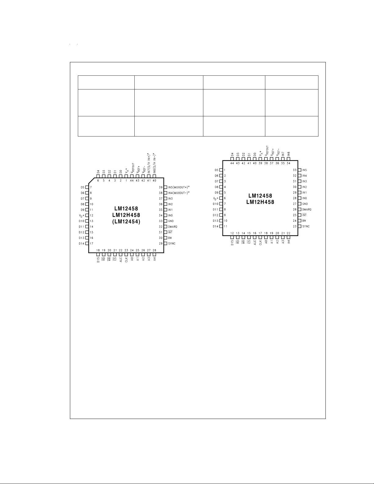
Connection Diagrams
Order Number LM12458CIVF or LM12H458CIVF
* Pin names in ( ) apply to the LM12454 and LM12H454.
DS011264-2
Order Number LM12454CIV,
LM12458CIV or LM12H458CIV
See NS Package Number V44A
Order Number LM12H458MEL/883 or 5962-9319502MYA
See NS Package Number EL44A
See NS Package Number VGZ44A
DS011264-34
www.national.com 2
Page 3
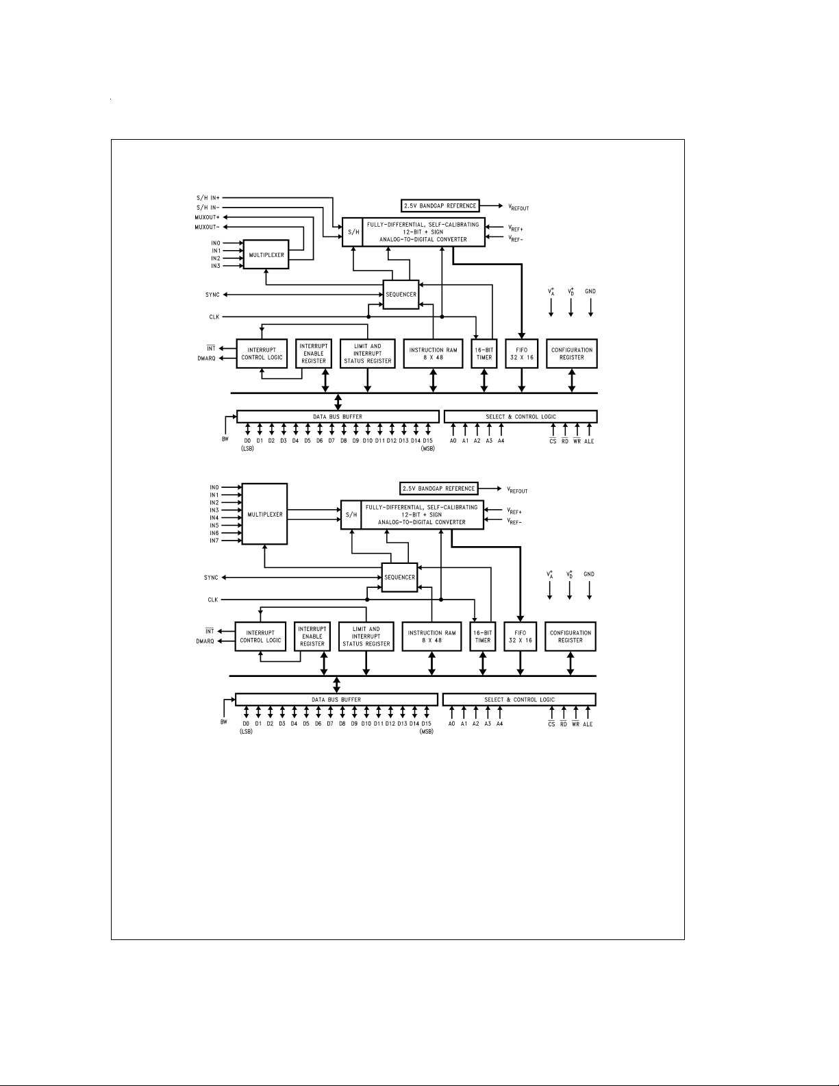
Functional Diagrams
LM12454
DS011264-1
LM12(H)458
DS011264-21
www.national.com3
Page 4
Absolute Maximum Ratings (Notes 1, 2)
If Military/Aerospace specified devices are required,
please contact the National Semiconductor Sales Office/
Distributors for availability and specifications.
Supply Voltage (V
Voltage at Input and Output Pins
except IN0–IN3 (LM12454) −0.3V to V
and IN0–IN7 (LM12(H)458)
Voltage at Analog Inputs IN0–IN3 (LM12454)
and IN0–IN7 (LM12(H)458) GND − 5V to V
+−VD+| 300 mV
|V
A
Input Current at Any Pin (Note 3)
Package Input Current (Note 3)
Power Dissipation (T
V Package (Note 4) 875 mW
Storage Temperature −65˚C to +150˚C
Lead Temperature
V Package, Infrared, 15 sec. +300˚C
EL and W Packages,
Solder, 10 sec. +250˚C
+ and VD+) 6.0V
A
+
+ 0.3V
+
±
5mA
±
=
25˚C)
A
20 mA
+5V
See AN-450 “Surface Mounting Methods and Their Effect on
Product Reliability” for other methods of soldering surface
mount devices.
Operating Ratings (Notes 1, 2)
Temperature Range
≤ TA≤ T
(T
min
LM12454CIV/
LM12(H)458CIV −40˚C ≤ T
LM12458MEL/883 −55˚C ≤ T
Supply Voltage
+, VD+ 3.0V to 5.5V
V
A
+−VD+| ≤100 mV
|V
A
Input Range GND ≤ V
V
IN+
Input Range GND ≤ V
V
IN−
Input Voltage 1V ≤ V
V
REF+
Input Voltage 0V ≤ V
V
REF−
V
REF+−VREF−
Common Mode
V
REF
Range (Note 16) 0.1 V
max
)
A
IN+
IN−
REF+
≤ V
REF−
REF+
1V ≤ V
REF
+
≤ V
A
REFCM
≤ 0.6 V
ESD Susceptibility (Note 5) 1.5 kV
LM12458MEL/883 2.0 kV
Converter Characteristics (Notes 6, 7, 8, 9, 19)
The following specifications apply to the LM12454, LM12458, and LM12H458 for VA+=VD+=5V, V
12-bit + sign conversion mode, f
and V
V
REF+
otherwise specified. Boldface limits apply for T
≤ 25Ω, fully-differential input with fixed 2.5V common-mode voltage, and minimum acquisition time unless
REF−
=
8.0 MHz (LM12H458) or f
CLK
A
=
5.0 MHz (LM12454/8), R
CLK
=
=
to T
T
T
J
MIN
; all other limits T
MAX
S
=
=
T
A
J
Symbol Parameter Conditions Typical Limits Unit
(Note 10) (Note 11) (Limit)
ILE Positive and Negative Integral After Auto-Cal (Notes 12, 17)
±
Linearity Error
TUE Total Unadjusted Error After Auto-Cal (Note 12)
±
Resolution with No Missing Codes After Auto-Cal (Note 12) 13 Bits (max)
DNL Differential Non-Linearity After Auto-Cal
Zero Error After Auto-Cal (Notes 13, 17)
LM12H458
Positive Full-Scale Error After Auto-Cal (Notes 12, 17)
±
±
LM12(H)458MEL
Negative Full-Scale Error After Auto-Cal (Notes 12, 17)
±
LM12(H)458MEL
DC Common Mode Error (Note 14)
±
ILE 8-Bit + Sign and “Watchdog” (Note 12)
Mode Positive and Negative
Integral Linearity Error
TUE 8-Bit + Sign and “Watchdog” Mode After Auto-Zero
±
Total Unadjusted Error
8-Bit + Sign and “Watchdog” Mode 9 Bits (max)
Resolution with No Missing Codes
DNL 8-Bit + Sign and “Watchdog” Mode
Differential Non-Linearity
8-Bit + Sign and “Watchdog” Mode After Auto-Zero
Zero Error
8-Bit + Sign and “Watchdog” Positive
and Negative Full-Scale Error
=
5V, V
REF+
=
25Ω, source impedance for
REF−
25˚C.
1/2
±
1 LSB (max)
1 LSB
3
±
⁄
4
LSB (max)
±
1
1/2
1/2
1/2
2
1/2
±
1.5 LSB (max)
±
2 LSB (max)
±
2.5
±
2 LSB (max)
±
2.5
±
3.5 LSB (max)
±
1/2 LSB (max)
±
3/4 LSB (max)
±
3/4 LSB (max)
±
1/2 LSB (max)
±
1/2 LSB (max)
≤ 85˚C
A
≤ 125˚C
≤ VA+
≤ VA+
≤ VA+
−1V
≤ VA+
=
0V,
+
A
www.national.com 4
Page 5
Converter Characteristics (Notes 6, 7, 8, 9, 19) (Continued)
The following specifications apply to the LM12454, LM12458, and LM12H458 for VA+=VD+=5V, V
12-bit + sign conversion mode, f
and V
V
REF+
otherwise specified. Boldface limits apply for T
≤ 25Ω, fully-differential input with fixed 2.5V common-mode voltage, and minimum acquisition time unless
REF−
=
8.0 MHz (LM12H458) or f
CLK
A
=
5.0 MHz (LM12454/8), R
CLK
=
=
to T
T
T
J
MIN
; all other limits T
MAX
S
=
=
T
A
J
Symbol Parameter Conditions Typical Limits Unit
(Note 10) (Note 11) (Limit)
8-Bit + Sign and “Watchdog” Mode
±
DC Common Mode Error
Multiplexer Channel-to-Channel
±
0.05 LSB
Matching
V
IN+
V
IN−
V
IN+−VIN−
Non-Inverting Input Range GND V (min)
Inverting Input Range GND V (min)
Differential Input Voltage Range −V
Common Mode Input Voltage Range GND V (min)
PSS Power Supply Zero Error V
Sensitivity Full-Scale Error V
(Note 15) Linearity Error
C
REF
C
IN
V
REF+/VREF−
Input Capacitance 85 pF
Selected Multiplexer Channel Input 75 pF
+=VD+=5V±10
A
=
4.5V, V
REF+
REF−
%
=
GND
±
±
±
Capacitance
=
5V, V
REF+
=
25Ω, source impedance for
REF−
25˚C.
1/8 LSB
V
+ V (max)
A
V
+ V (max)
A
+
A
V
+ V (max)
A
V
+ V (max)
A
0.2
0.4
±
1.75 LSB (max)
±
2 LSB (max)
0.2 LSB
=
0V,
V (min)
Converter AC Characteristics (Notes 6, 7, 8, 9, 19)
The following specifications apply to the LM12454, LM12458, and LM12H458 for VA+=VD+=5V, V
12-bit + sign conversion mode, f
and V
V
REF+
otherwise specified. Boldface limits apply for T
≤ 25Ω, fully-differential input with fixed 2.5V common-mode voltage, and minimum acquisition time unless
REF−
=
8.0 MHz (LM12H458) or f
CLK
A
=
5.0 MHz (LM12454/8), R
CLK
=
=
to T
T
T
J
MIN
; all other limits T
MAX
S
=
=
T
A
J
=
5V, V
REF+
=
25Ω, source impedance for
25˚C.
Symbol Parameter Conditions Typical Limits Unit
(Note 10) (Note 11) (Limit)
Clock Duty Cycle 50
40
60
t
C
Conversion Time 13-Bit Resolution, 44 (t
Sequencer State S5 (
Figure 15
)
9-Bit Resolution, 21 (t
Sequencer State S5 (
t
A
Acquisition Time Sequencer State S7 (
Figure 15
Figure 15
)
)9(t
) 44 (t
CLK
) 21 (t
CLK
) 9(t
CLK
)+50ns (max)
CLK
)+50ns (max)
CLK
)+50ns (max)
CLK
Built-in minimum for 13-Bits
Built-in minimum for 9-Bits and 2 (t
) 2(t
CLK
)+50ns (max)
CLK
“Watchdog” mode
t
Z
t
CAL
Auto-Zero Time Sequencer State S2 (
Full Calibration Time Sequencer State S2 (
Figure 15
Figure 15
)76(t
) 4944 (t
CLK
CLK
) 76 (t
) 4944 (t
)+50ns (max)
CLK
)+50ns (max)
CLK
Throughput Rate 89 88 kHz
(Note 18) LM12H458 142 140 (min)
t
WD
“Watchdog” Mode Comparison Sequencer States S6, S4, 11 (t
Time and S5 (
Figure 15
)
) 11 (t
CLK
)+50ns (max)
CLK
REF−
=
0V,
%
(max)
%
(min)
%
www.national.com5
Page 6
Converter AC Characteristics (Notes 6, 7, 8, 9, 19) (Continued)
The following specifications apply to the LM12454, LM12458, and LM12H458 for VA+=VD+=5V, V
12-bit + sign conversion mode, f
and V
V
REF+
otherwise specified. Boldface limits apply for T
≤ 25Ω, fully-differential input with fixed 2.5V common-mode voltage, and minimum acquisition time unless
REF−
=
8.0 MHz (LM12H458) or f
CLK
A
=
5.0 MHz (LM12454/8), R
CLK
=
=
to T
T
T
J
MIN
; all other limits T
MAX
S
=
=
T
A
J
=
5V, V
REF+
=
25Ω, source impedance for
25˚C.
Symbol Parameter Conditions Typical Limits Unit
(Note 10) (Note 11) (Limit)
=
±
DSNR Differential Signal-to-Noise Ratio V
SESNR Single-Ended Signal-to-Noise V
Ratio f
DSINAD Differential Signal-to-Noise + V
Distortion Ratio f
SESINAD Single-Ended Signal-to-Noise + V
Distortion Ratio f
DTHD Differential Total Harmonic V
Distortion f
SETHD Single-Ended Total Harmonic V
Distortion f
DENOB Differential Effective Number V
of Bits f
SEENOB Single-Ended Effective Number V
of Bits f
DSFDR Differential Spurious Free V
Dynamic Range f
Multiplexer Channel-to-Channel V
Crosstalk f
5V
IN
=
f
1 kHz 77.5 dB
IN
=
f
20 kHz 75.2 dB
IN
=
f
40 kHz 74.7 dB
IN
=
5V
IN
p-p
=
1 kHz 69.8 dB
IN
=
f
20 kHz 69.2 dB
IN
=
f
40 kHz 66.6 dB
IN
=
±
5V
IN
=
1 kHz 76.9 dB
IN
=
f
20 kHz 73.9 dB
IN
=
f
40 kHz 70.7 dB
IN
=
5V
IN
p-p
=
1 kHz 69.4 dB
IN
=
f
20 kHz 68.3 dB
IN
=
f
40 kHz 65.7 dB
IN
=
±
5V
IN
=
1 kHz −85.8 dB
IN
=
f
20 kHz −79.9 dB
IN
=
f
40 kHz −72.9 dB
IN
=
5V
IN
p-p
=
1 kHz −80.3 dB
IN
=
f
20 kHz −75.6 dB
IN
=
f
40 kHz −72.8 dB
IN
=
±
5V
IN
=
1 kHz 12.6 Bits
IN
=
f
20 kHz 12.2 Bits
IN
=
f
40 kHz 12.1 Bits
IN
=
5V
IN
p-p
=
1 kHz 11.3 Bits
IN
=
f
20 kHz 11.2 Bits
IN
=
f
40 kHz 10.8 Bits
IN
=
±
5V
IN
=
1 kHz 87.2 dB
IN
=
f
20 kHz 78.9 dB
IN
=
f
40 kHz 72.8 dB
IN
=
5V
IN
PP
=
40 kHz
IN
LM12454 MUXOUT Only −76 dB
LM12(H)458 MUX −78 dB
plus Converter
t
PU
t
WU
Power-Up Time 10 ms
Wake-Up Time 10 ms
REF−
=
0V,
www.national.com 6
Page 7
DC Characteristics (Notes 6, 7, 8, 19)
The following specifications apply to the LM12454, LM12458, and LM12H458 for VA+=VD+=5V, V
=
f
8.0 MHz (LM12H454/8) or f
CLK
face limits apply for T
=
T
A
J
=
5.0 MHz (LM12458), and minimum acquisition time unless otherwise specified. Bold-
CLK
=
to T
T
MIN
; all other limits T
MAX
=
=
T
25˚C.
A
J
REF+
=
5V, V
Symbol Parameter Conditions Typical Limits Unit
(Note 10) (Note 11) (Limit)
+VD+ Supply Current CS=“1”
I
D
LM12454/8 0.55 1.0 mA (max)
LM12H458 0.55 1.2
I
+V
A
+ Supply Current CS=“1”
A
LM12454/8 3.1 5.0 mA (max)
LM12H458 3.1 5.5
I
ST
Stand-By Supply Current (ID++IA+) Power-Down Mode Selected
Clock Stopped 10 µA (max)
8 MHz Clock 40 µA (max)
Multiplexer ON-Channel Leakage Current V
+=5.5V
A
ON-Channel=5.5V 0.3
OFF-Channel=0V 0.1 µA (max)
LM12(H)458MEL 0.5
ON-Channel=0V 0.3
OFF-Channel=5.5V 0.1 µA (max)
LM12(H)458MEL 0.5
Multiplexer OFF-Channel Leakage Current V
+=5.5V
A
ON-Channel=5.5V 0.3
OFF-Channel=0V 0.1 µA (max)
LM12(H)458MEL 0.5
ON-Channel=0V 0.3
OFF-Channel=5.5V 0.1 µA (max)
LM12(H)458MEL 0.5
R
Multiplexer ON-Resistance LM12454
ON
=
V
5V 800 1500 Ω(max)
IN
=
V
2.5V 850 1500 Ω(max)
IN
=
V
0V 760 1500 Ω(max)
IN
Multiplexer Channel-to-Channel LM12454
R
matching V
ON
=
5V
IN
=
V
2.5V
IN
=
V
0V
IN
±
1.0
±
1.0
±
1.0
±
%
%
%
%
3.0
±
%
3.0
±
%
3.0
REF−
=
0V,
(max)
(max)
(max)
Internal Reference Characteristics (Notes 6, 7, 19)
The following specifications apply to the LM12454, LM12458, and LM12H458 for VA+=VD+=5V unless otherwise specified.
Boldface limits apply for T
Symbol Parameter Conditions Typical Limits Unit
V
REFOUT
∆V
Internal Reference Output Voltage 2.5 2.5±4
/∆T Internal Reference Temperature 40 ppm/˚C
REF
Coefficient
∆
/∆ILInternal Reference Load Regulation Sourcing (0<IL≤ +4 mA) 0.2
REF
∆V
I
∆V
SC
Line Regulation 4.5V ≤ VA+ ≤ 5.5V 3 20 mV (max)
REF
Internal Reference Short Circuit Current V
/∆t Long Term Stability 200 ppm/kHr
REF
=
=
to T
T
A
T
J
MIN
; all other limits T
MAX
=
=
T
A
25˚C.
J
(Note 10) (Note 11) (Limit)
%
V (max)
±
LM12(H)458MEL 2.5
Sinking (−1 ≤ I
REFOUT
<
0 mA) 1.2
IL
=
0V 13 25 mA (max)
%
6
%
/mA (max)
%
/mA (max)
www.national.com7
Page 8
Internal Reference Characteristics (Notes 6, 7, 19) (Continued)
The following specifications apply to the LM12454, LM12458, and LM12H458 for VA+=VD+=5V unless otherwise specified.
Boldface limits apply for T
Symbol Parameter Conditions Typical Limits Unit
t
SU
Internal Reference Start-Up Time VA+=VD+=0V→5V 10 ms
=
=
to T
T
A
T
J
MIN
; all other limits T
MAX
=
=
T
25˚C.
A
J
(Note 10) (Note 11) (Limit)
=
C
100 µF
L
Digital Characteristics (Notes 6, 7, 8, 19)
The following specifications apply to the LM12454, LM12458, and LM12H458 for VA+=VD+=5V, unless otherwise specified. Boldface limits apply for T
Symbol Parameter Conditions Typical Limits Unit
V
V
I
IN(1)
I
IN(0)
C
V
V
I
OUT
IN(1)
IN(0)
IN
OUT(1)
OUT(0)
Logical “1” Input Voltage VA+=VD+=5.5V 2.0 V (min)
Logical “0” Input Voltage VA+=VD+=4.5V 0.8 V (max)
Logical “1” Input Current V
Logical “0” Input Current V
D0–D15 Input Capacitance 6 pF
Logical “1” Output Voltage VA+=VD+=4.5V
Logical “0” Output Voltage VA+=VD+=4.5V 0.4 V (max)
TRI-STATE®Output Leakage Current V
=
=
to T
T
T
A
J
MIN
; all other limits T
MAX
=
=
T
25˚C.
A
J
(Note 10) (Note 11) (Limit)
=
5V 0.005 1.0 µA (max)
IN
LM12(H)458MEL 2.0
=
0V −0.005 −1.0 µA (max)
IN
LM12(H)458MEL −2.0
=
I
−360 µA 2.4 V (min)
OUT
=
I
−10 µA 4.25 V (min)
OUT
=
I
1.6 mA
OUT
=
0V −0.01 −3.0 µA (max)
OUT
=
V
5V 0.01 3.0 µA (max)
OUT
Digital Timing Characteristics (Notes 6, 7, 8, 19)
The following specifications apply to the LM12454, LM12458, and LM12H458 for VA+=VD+=5V, t
100 pF on data I/O, INT and DMARQ lines unless otherwise specified. Boldface limits apply for T
other limits T
Figures 8, 9, 10
(See
www.national.com 8
=
=
T
25˚C.
A
J
Symbol Parameter Conditions Typical Limits Unit
) (Note 10) (Note 11) (Limit)
1, 3 CS or Address Valid to ALE Low
Set-Up Time
2, 4 CS or Address Valid to ALE Low
Hold Time
5 ALE Pulse Width 45 ns (min)
6 RD High to Next ALE High
7 ALE Low to RD Low
8 RD Pulse Width
9 RD High to Next RD or WR Low
10 ALE Low to WR Low
11 WR Pulse Width
12 WR High to Next ALE High
13 WR High to Next RD or WR Low
14 Data Valid to WR High Set-Up Time
15 Data Valid to WR High Hold Time
16 RD Low to Data Bus Out of TRI-STATE
=
r
A
t
f
=
T
=
3 ns, and C
=
T
J
MIN
to T
MAX
=
L
; all
40 ns (min)
20 ns (min)
35 ns (min)
20 ns (min)
100 ns (min)
100 ns (min)
20 ns (min)
60 ns (min)
75 ns (min)
140 ns (min)
40 ns (min)
30 ns (min)
40 10 ns (min)
70 ns (max)
Page 9
Digital Timing Characteristics (Notes 6, 7, 8, 19) (Continued)
=
The following specifications apply to the LM12454, LM12458, and LM12H458 for VA+=VD+=5V, t
100 pF on data I/O, INT and DMARQ lines unless otherwise specified. Boldface limits apply for T
other limits T
=
=
T
25˚C.
A
J
r
A
t
f
=
T
=
3 ns, and C
=
T
J
MIN
Symbol Parameter Conditions Typical Limits Unit
Figures 8, 9, 10
(See
17 RD High to TRI-STATE
) (Note 10) (Note 11) (Limit)
=
R
1kΩ 30 10 ns (min)
L
110 ns (max)
18 RD Low to Data Valid (Access Time)
30 10 ns (min)
80 ns (max)
20 Address Valid or CS Low to RD Low
21 Address Valid or CS Low to WR Low
20 ns (min)
20 ns (min)
19 Address Invalid 10 ns (min)
from RD or WR High
22 INT High from RD Low 30 10 ns (min)
60 ns (max)
23 DMARQ Low from RD Low
30 10 ns (min)
60 ns (max)
Note 1: Absolute Maximum Ratings indicate limits beyond which damage to the device may occur.Operating Ratings indicate conditions for which the device is func-
tional, but do not guarantee specific performance limits. For guaranteed specifications and test conditions, see the Electrical Characteristics. The guaranteed specifications apply only for the test conditions listed. Some performance characteristics may degrade when the device is not operated under the listed test conditions.
Note 2: All voltages are measured with respect to GND, unless otherwise specified.
Note 3: When the input voltage (V
The 20 mA maximum package input current rating allows the voltage at any four pins, with an input current of 5 mA, to simultaneously exceed the power supply voltages.
Note 4: The maximum power dissipation must be derated at elevated temperatures and is dictated by T
to ambient thermal resistance), and T
ber given in the Absolute Maximum Ratings, whichever is lower. For this device, T
LM12(H)458 in the V package, when board mounted, is 47˚C/W, in the W package, when board mounted, is 50˚C/W (θJ
board mounted, is 70˚C/W (θJ
Note 5: Human body model, 100 pF discharged through a 1.5 kΩ resistor.
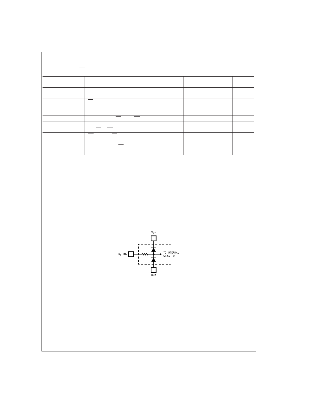
Note 6: Two on-chip diodes are tied to each analog input through a series resistor, as shown below. Input voltage magnitude up to 5V above V
will not damage the LM12454 or the LM12(H)458. However, errors in the A/D conversion can occur if these diodes are forward biased by more than 100 mV.As an
example, if V
+ is 4.5 VDC, full-scale input voltage must be ≤4.6 VDCto ensure accurate conversions.
A
) at any pin exceeds the power supply rails (V
IN
(ambient temperature). The maximum allowable power dissipation at any temperature is PD
A
=
3.5˚C/W).
C
<
IN
Jmax
>
GND or V
(VA+orVD+)), the current at that pin should be limited to 5 mA.
IN
(maximum junction temperature), θJA(package junction
Jmax
=
150˚C, and the typical thermal resistance (θ
=
(T
max
Jmax−TA
) of the LM12454 and
=
5.8˚C/W), and in the EL package, when
C
JA
+ or 5V below GND
A
=
L
to T
MAX
)/θJAor the num-
; all
DS011264-3
+ and VD+ must be connected together to the same power supply voltage and bypassed with separate capacitors at each V+pin to assure conversion/
Note 7: V
A
comparison accuracy.
Note 8: Accuracy is guaranteed when operating at f
Note 9: With the test condition for V
Note 10: Typicals are at T
Note 11: Limits are guaranteed to National’s AOQL (Average Output Quality Level).
Note 12: Positive integral linearity error is defined as the deviation of the analog value, expressed in LSBs, from the straight line that passes through positive
full-scale and zero. For negative integral linearity error the straight line passes through negative full-scale and zero. (See
Note 13: Zero error is a measure of the deviation from the mid-scale voltage (a code of zero), expressed in LSB. It is the worst-case value of the code transitions
between −1 to 0 and 0 to +1 (see
Note 14: The DC common-mode error is measured with both inputs shorted together and driven from 0V to 5V.The measured value is referred to the resulting out-
put value when the inputs are driven with a 2.5V signal.
Note 15: Power Supply Sensitivity is measured after Auto-Zero and/or Auto-Calibration cycle has been completed with V
Note 16: V
(Reference Voltage Common Mode Range) is defined as (V
REFCM
REF(VREF+−VREF−
=
25˚C and represent most likely parametric norm.
A
Figure 8
).
=
5 MHz for the LM12454/8 and f
CLK
) given as +5V, the 12-bit LSB is 1.22 mV and the 8-bit/“Watchdog” LSB is 19.53 mV.
REF++VREF−
=
8 MHz for the LM12H458.
CLK
)/2.
Figure 6 Figure 7
+ and VD+ at the specified extremes.
A
).
www.national.com9
Page 10
Digital Timing Characteristics (Notes 6, 7, 8, 19) (Continued)
Note 17: The LM12(H)454/8’s self-calibration technique ensures linearity and offset errors as specified, but noise inherent in the self-calibration process will result
in a repeatability uncertainty of
Note 18: The Throughput Rate is for a single instruction repeated continuously. Sequencer states 0 (1 clock cycle), 1 (1 clock cycle), 7 (9 clock cycles) and 5 (44
clock cycles) are used (see
version. The Throughput Rate is f
Note 19: A military RETS specification is available upon request.
±
0.10 LSB.
Figure 15
). One additional clock cycle is used to read the conversion result stored in the FIFO, for a total of 56 clock cycles per con-
(MHz)/N, where N is the number of clock cycles/conversion.
CLK
Electrical Characteristics
=
V
V
REF
REF+−VREF−
=
V
V
IN
IN+−VIN−
GND ≤ V
GND ≤ V
IN+≤VA
IN−≤VA
+
+
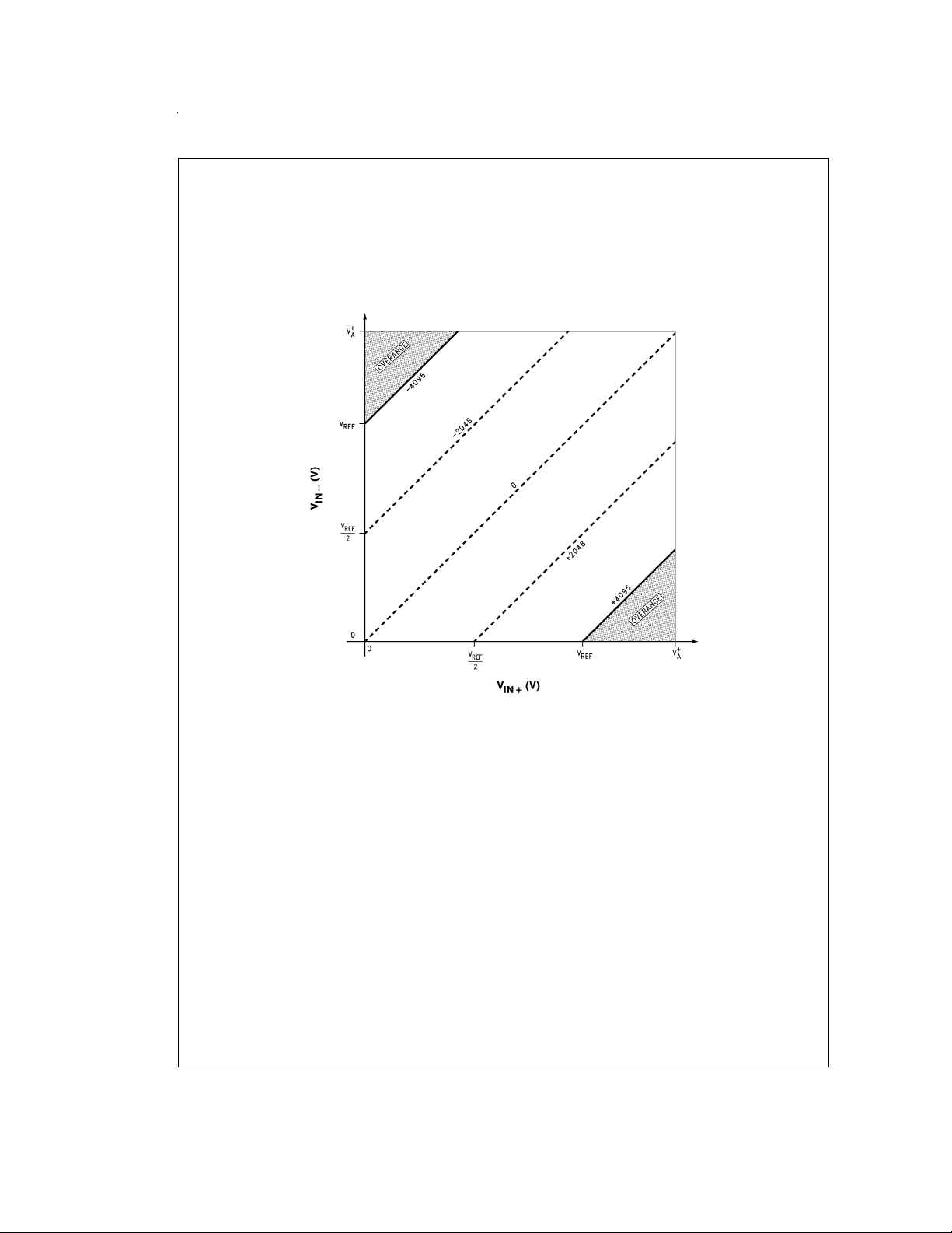
FIGURE 1. The General Case of Output Digital Code vs the Operating Input Voltage Range
www.national.com 10
DS011264-22
Page 11
Electrical Characteristics (Continued)
=
V
IN+−VIN−
IN+≤VA
IN−≤VA
=
+
+
4.096V
V
REF+−VREF−
V
IN
GND ≤ V
GND ≤ V
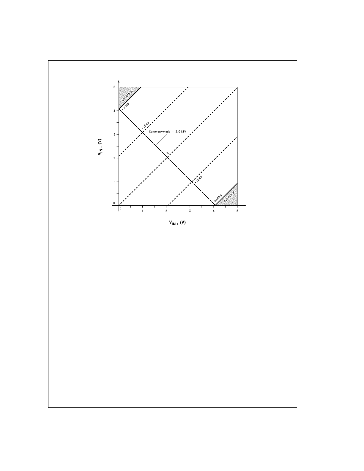
FIGURE 2. Specific Case of Output Digital Code vs the Operating Input Voltage Range for V
DS011264-23
REF
=
4.096V
www.national.com11
Page 12
Electrical Characteristics (Continued)
V
REF
=
V
REF+−VREF−
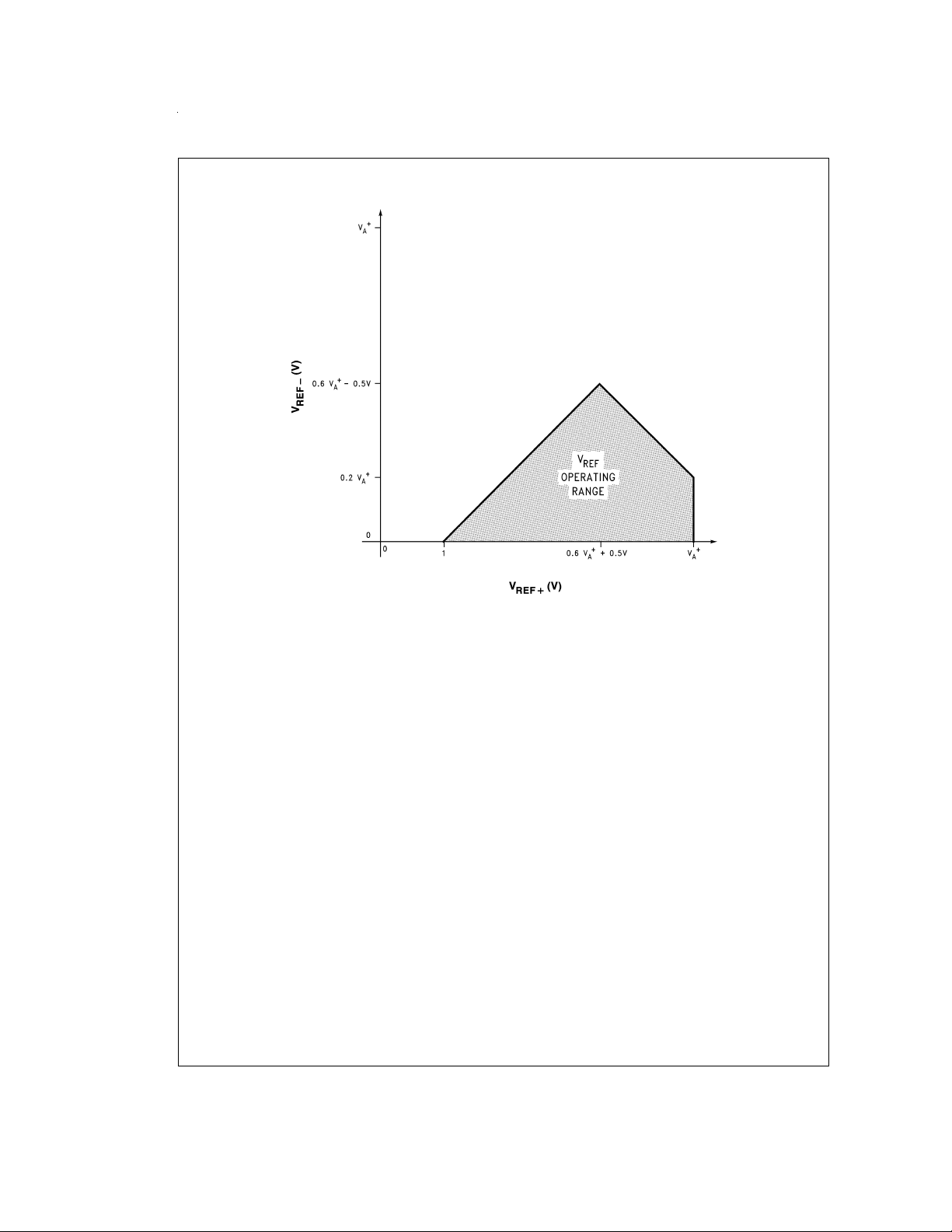
FIGURE 3. The General Case of the V
Operating Range
REF
DS011264-24
www.national.com 12
Page 13
Electrical Characteristics (Continued)
=
V
REF
VA+=5V
V
REF+−VREF−
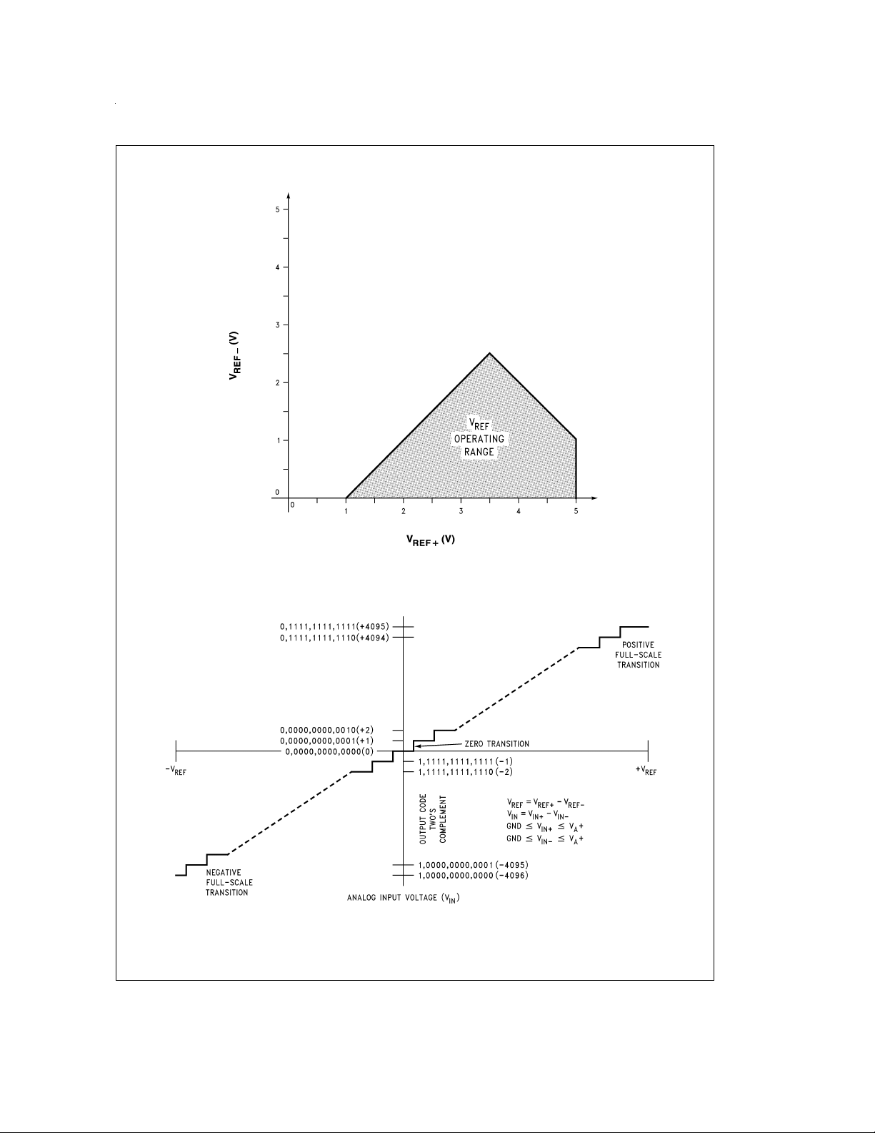
FIGURE 4. The Specific Case of the V
FIGURE 5. Transfer Characteristic
Operating Range for VA+=5V
REF
DS011264-25
DS011264-4
www.national.com13
Page 14

Electrical Characteristics (Continued)
FIGURE 6. Simplified Error Curve vs Output Code without Auto-Calibration or Auto-Zero Cycles
DS011264-5
FIGURE 7. Simplified Error Curve vs Output Code after Auto-Calibration Cycle
FIGURE 8. Offset or Zero Error Voltage
www.national.com 14
DS011264-6
DS011264-7
Page 15

Typical Performance Characteristics (Note 9) The following curves apply for 12-bit + sign mode after
auto-calibration unless otherwise specified. The performance for 8-bit + sign and “watchdog” modes is equal to or better than
shown.
Linearity Error Change
vs Clock Frequency
Linearity Error Change
vs Supply Voltage
Full-Scale Error Change
vs Reference Voltage
DS011264-37
DS011264-40
Linearity Error Change
vs Temperature
Full-Scale Error Change
vs Clock Frequency
Full-Scale Error
vs Supply Voltage
DS011264-38
DS011264-41
Linearity Error Change
vs Reference Voltage
DS011264-39
Full-Scale Error Change
vs Temperature
DS011264-42
Zero Error Change
vs Clock Frequency
DS011264-43
DS011264-44
DS011264-45
www.national.com15
Page 16

Typical Performance Characteristics (Note 9) The following curves apply for 12-bit + sign mode after
auto-calibration unless otherwise specified. The performance for 8-bit + sign and “watchdog” modes is equal to or better than
shown. (Continued)
Zero Error Change
vs Temperature
Analog Supply Current
vs Temperature
V
Load Regulation
REFOUT
DS011264-46
DS011264-49
Zero Error Change
vs Reference Voltage
Digital Supply Current
vs Clock Frequency
V
REFOUT
DS011264-47
DS011264-50
Line Regulation
Zero Error Change
vs Supply Voltage
DS011264-48
Digital Supply Current
vs Temperature
DS011264-51
DS011264-52
www.national.com 16
DS011264-53
Page 17

Typical Dynamic Performance Characteristics The following curves apply for 12-bit + sign
mode after auto-calibration unless otherwise specified.
Bipolar Signal-to-Noise Ratio
vs Input Frequency
DS011264-54
Bipolar Spectral Response
with 1.028 kHz Sine Wave Input
DS011264-57
Bipolar Signal-to-Noise
+ Distortion Ratio
vs Input Frequency
Bipolar Spectral Response
with 10 kHz Sine Wave Input
DS011264-58
DS011264-55
Bipolar Signal-to-Noise
+ Distortion Ratio
vs Input Signal Level
DS011264-56
Bipolar Spectral Response
with 20 kHz Sine Wave Input
DS011264-59
Bipolar Spectral Response
with 40 kHz Sine Wave Input
DS011264-60
Bipolar Spurious Free
Dynamic Range
DS011264-61
Unipolar Signal-to-Noise Ratio
vs Input Frequency
DS011264-62
www.national.com17
Page 18

Typical Dynamic Performance Characteristics The following curves apply for 12-bit + sign
mode after auto-calibration unless otherwise specified. (Continued)
Unipolar Signal-to-Noise
+ Distortion Ratio
vs Input Frequency
DS011264-63
Unipolar Spectral Response
with 10 kHz Sine Wave Input
DS011264-66
Unipolar Signal-to-Noise
+ Distortion Ratio
vs Input Signal Level
Unipolar Spectral Response
with 20 kHz Sine Wave Input
Test Circuits and Waveforms
DS011264-64
DS011264-67
Unipolar Spectral Response
with 1.028 kHz Sine Wave Input
DS011264-65
Unipolar Spectral Response
with 40 kHz Sine Wave Input
DS011264-68
DS011264-12
DS011264-14
FIGURE 9. TRI-STATE Test Circuits and Waveforms
www.national.com 18
DS011264-13
DS011264-15
Page 19

Timing Diagrams V
+=VD+=+5V, t
A
FIGURE 10. Multiplexed Data Bus
1, 3: CS or Address valid to ALE low set-up time.
2, 4: CS or Address valid to ALE low hold time.
5: ALE pulse width
6: RD high to next ALE high
7: ALE low to RD low
8: RD pulse width
9: RD high to next RD or WR low
10: ALE low to WR low
=
=
t
R
F
3 ns, C
=
100 pF for the INT, DMARQ, D0–D15 outputs.
L
DS011264-16
11: WR pulse width
12: WR high to next ALE high
13: WR high to next WR or RD low
14: Data valid to WR high set-up time
15: Data valid to WR high hold time
16: RD low to data bus out of TRI-STATE
17: RD high to TRI-STATE
18: RD low to data valid (access time)
www.national.com19
Page 20

Timing Diagrams V
outputs. (Continued)
+=VD+=+5V, t
A
=
=
t
R
F
3 ns, C
=
100 pF for the INT, DMARQ, D0–D15
L
FIGURE 11. Non-Multiplexed Data Bus (ALE=1)
8: RD pulse width
9: RD high to next RD or WR low
11: WR pulse width
13: WR high to next WR or RD low
14: Data valid to WR high set-up time
15: Data valid to WR high hold time
VA+=VD+=+5V, t
=
t
R
F
3 ns, C
=
100 pF for the INT, DMARQ, D0–D15 outputs.
L
=
FIGURE 12. Interrupt and DMARQ
22: INT high from RD low
23: DMARQ low from RD low
www.national.com 20
DS011264-17
16: RD low to data bus out of TRI-STATE
17: RD high to TRI-STATE
18: RD low to data valid (access time)
19: Address invalid from RD or WR high (hold time)
20: CS low or address valid to RD low
21: CS low or address valid to WR low
DS011264-18
Page 21

Pin Description
VA+VD+ Analog and digital supply voltage pins. The
D0–D15 The internal data input/output TRI-STATE buffers
RD
WR
CS
ALE Address Latch Enable input. It is used in systems
CLK External clock input pin. The LM12(H)454/8 oper-
A0–A4 The LM12(H)454/8’s address lines. They are
SYNC Synchronization input/output. When used as an
LM12(H)454/8’s supply voltage operating range
is +3.0V to +5.5V.Accuracy is guaranteed only if
V
+ and VD+ are connected to the same power
A
supply.Each pin should have a parallel combination of 10 µF (electrolytic or tantalum) and 0.1 µF
(ceramic) bypass capacitors connected between
it and ground.
are connected to these pins. These buffers are
designed to drive capacitive loads of 100 pF or
less. External buffers are necessary for driving
higher load capacitances. These pins allows the
user a means of instruction input and data output. With a logic high applied to the BW pin, data
lines D8–D15 are placed in a high impedance
state and data lines D0–D7 are used for instruction input and data output when the
LM12(H)454/8 is connected to an 8-bit wide data
bus. A logic low on the BW pin allows the
LM12(H)454/8 to exchange information over a
16-bit wide data bus.
Input for the active low READ bus control signal.
The data input/output TRI-STATE buffers, as selected by the logic signal applied to the BW pin,
are enabled when RD and CS are both low. This
allows the LM12(H)454/8 to transmit information
onto the databus.
Input for the active low WRITE bus control signal.
The data input/output TRI-STATE buffers, as selected by the logic signal applied to the BW pin,
are enabled when WR and CS are both low. This
allows the LM12(H)454/8 to receive information
from the databus.
Input for the active low Chip Select control signal.
A logic low should be applied to this pin only during a READ or WRITE access to the
LM12(H)454/8. The internal clocking is halted
and conversion stops while Chip Select is low.
Conversion resumes when the Chip Select input
signal returns high.
containing a multiplexed databus. When ALE is
asserted high, the LM12(H)454/8 accepts information on the databus as a valid address. A
high-to-low transition will latch the address data
on A0–A4 while the CS is low. Any changes on
A0–A4 and CS while ALE is low will not affect the
LM12(H)454/8. See
Figure 10
. When a
non-multiplexed bus is used, ALE is continuously
asserted high. See
Figure 11
.
ates with an input clock frequency in the range of
0.05 MHz to 10.0 MHz.
used to access all internal registers, Conversion
FIFO, and Instruction RAM.
output, it is designed to drive capacitive loads of
100 pF or less. External buffers are necessary for
driving higher load capacitances. SYNC is an in-
put if the Configuration register’s “I/O Select” bit
is low. A rising edge on this pin causes the inter-
nal S/H to hold the input signal. The next rising
clock edge either starts a conversion or makes a
comparison to a programmable limit depending
on which function is requested by a programming
instruction. This pin will be an output if “I/O Select” is set high. The SYNC output goes high
when a conversion or a comparison is started
and low when completed. (See Section 2.2). An
internal reset after power is first applied to the
LM12(H)454/8 automatically sets this pin as an
input.
BW Bus Width input pin. This input allows the
LM12(H)454/8 to interface directly with either an
8- or 16-bit databus.A logic high sets the width to
8 bits and places D8–D15 in a high impedance
state. A logic low sets the width to 16 bits.
INT
Active low interrupt output. This output is designed to drive capacitive loads of 100 pF or less.
External buffers are necessary for driving higher
load capacitances. An interrupt signal is generated any time a non-masked interrupt condition
takes place. There are eight different conditions
that can cause an interrupt. Any interrupt is reset
by reading the Interrupt Status register. (See
Section 2.3.)
DMARQ Active high Direct Memory Access Request out-
put. This output is designed to drive capacitive
loads of 100 pF or less. External buffers are necessary for driving higher load capacitances. It
goes high whenever the number of conversion
results in the conversion FIFO equals a programmable value stored in the Interrupt Enable register. It returns to a logic low when the FIFO is
empty.
GND LM12(H)454/8 ground connection. It should be
connected to a low resistance and inductance
analog ground return that connects directly to the
system power supply ground.
IN0–IN7
(IN0–IN3
LM12H454
LM12454)
The eight (LM12(H)458) or four (LM12454)
analog inputs. A given channel is selected
through the instruction RAM. Any of the channels can be configured as an independent
single-ended input. Any pair of channels,
whether adjacent or non-adjacent, can operate
as a fully differential pair.
S/H IN+
S/H IN−
MUXOUT+
MUXOUT−
V
REF−
The LM12454’s non-inverting and inverting inputs to the internal S/H.
The LM12454’s non-inverting and inverting outputs from the internal multiplexer.
The negative reference input. The
LM12(H)454/8 operate with 0V ≤ V
V
. This pin should be bypassed to ground
REF+
with a parallel combination of 10 µF and 0.1 µF
REF−
(ceramic) capacitors.
V
REF+
The positive reference input. The
LM12(H)454/8 operate with 0V ≤ V
This pin should be bypassed to ground with a
REF+
≤ VA+.
parallel combination of 10 µF and 0.1 µF (ceramic) capacitors.
V
REFOUT
The internal 2.5V bandgap’s output pin. This
pin should be bypassed to ground with a 100
µF capacitor.
≤
www.national.com21
Page 22

Application Information
1.0 Functional Description
The LM12454 and LM12(H)458 are multi-functional Data Acquisition Systems that include a fully differential
12-bit-plus-sign self-calibrating analog-to-digital converter
(ADC) with a two’s-complement output format, an 8-channel
(LM12(H)458) or a 4-channel (LM12454) analog multiplexer,
an internal 2.5V reference, a first-in-first-out (FIFO) register
that can store 32 conversion results, and an Instruction RAM
that can store as many as eight instructions to be sequentially executed. The LM12454 also has a differential multiplexer output and a differential S/H input. All of this circuitry
operates on only a single +5V power supply.
The LM12(H)454/8 have three modes of operation:
12-bit + sign with correction
8-bit + sign without correction
8-bit + sign comparison mode (“watchdog” mode)
The fully differential 12-bit-plus-sign ADC uses a charge redistribution topology that includes calibration capabilities.
Charge re-distribution ADCs use a capacitor ladder in place
of a resistor ladder to form an internal DAC. The DAC is used
by a successive approximation register to generate intermediate voltages between the voltages applied to V
V
. These intermediate voltages are compared against
REF+
the sampled analog input voltage as each bit is generated.
The number of intermediate voltages and comparisons
equals the ADC’s resolution. The correction of each bit’s accuracy is accomplished by calibrating the capacitor ladder
used in the ADC.
Two different calibration modes are available; one compensates for offset voltage, or zero error,while the other corrects
both offset error and the ADC’s linearity error.
When correcting offset only, the offset error is measured
once and a correction coefficient is created. During the full
calibration, the offset error is measured eight times, averaged, and a correction coefficient is created. After completion of either calibration mode, the offset correction coefficient is stored in an internal offset correction register.
The LM12(H)454/8’s overall linearity correction is achieved
by correcting the internal DAC’s capacitor mismatch. Each
capacitor is compared eight times against all remaining
smaller value capacitors and any errors are averaged. Acorrection coefficient is then created and stored in one of the
thirteen internal linearity correction registers. An internal
state machine, using patterns stored in an internal 16 x 8-bit
ROM, executes each calibration algorithm.
Once calibrated, an internal arithmetic logic unit (ALU) uses
the offset correction coefficient and the 13 linearity correction
coefficients to reduce the conversion’s offset error and linearity error, in the background, during the 12-bit + sign conversion. The 8-bit + sign conversion and comparison modes
use only the offset coefficient. The 8-bit + sign mode performs a conversion in less than half the time used by the
12-bit + sign conversion mode.
The LM12(H)454/8’s “watchdog” mode is used to monitor a
single-ended or differential signal’s amplitude. Each
sampled signal has two limits.An interrupt can be generated
if the input signal is above or below either of the two limits.
This allows interrupts to be generated when analog voltage
inputs are “inside the window” or, alternatively, “outside the
window”. After a “watchdog” mode interrupt, the processor
can then request a conversion on the input signal and read
the signal’s magnitude.
REF−
and
The analog input multiplexer can be configured for any combination of single-ended or fully differential operation. Each
input is referenced to ground when a multiplexer channel operates in the single-ended mode. Fully differential analog input channels are formed by pairing any two channels together.
The LM12454’s multiplexer outputs and S/H inputs (MUXOUT+, MUXOUT− and S/H IN+, S/H IN−) provide the option
for additional analog signal processing. Fixed-gain amplifiers, programmable-gain amplifiers, filters, and other processing circuits can operate on the signal applied to the selected multiplexer channel(s). If external processing is not
used, connect MUXOUT+ to S/H IN+ and MUXOUT− to
S/H IN−.
The LM12(H)454/8’s internal S/H is designed to operate at
its minimum acquisition time (1.13 µs, 12 bits) when the
source impedance, R
<
RS≤ 4.17 kΩ, the internal S/H’s acquisition time can be increased to a maximum of 4.88 µs (12 bits, f
See Section 2.1 (Instruction RAM “00”) Bits 12–15 for more
,is≤60Ω (f
S
≤ 8 MHz). When 60Ω
CLK
CLK
=
8 MHz).
information.
An internal 2.5V bandgap reference output is available at pin
44. This voltage can be used as the ADC reference for ratiometric conversion or as a virtual ground for front-end analog
conditioning circuits. The V
to ground with a 100 µF capacitor.
pin should be bypassed
REFOUT
Microprocessor overhead is reduced through the use of the
internal conversion FIFO. Thirty-two consecutive conversions can be completed and stored in the FIFO without any
microprocessor intervention. The microprocessor can, at any
time, interrogate the FIFO and retrieve its contents. It can
also wait for the LM12(H)454/8 to issue an interrupt when
the FIFO is full or after any number (≤32) of conversions
have been stored.
Conversion sequencing, internal timer interval, multiplexer
configuration, and many other operations are programmed
and set in the Instruction RAM.
A diagnostic mode is available that allows verification of the
LM12(H)458’s operation. The diagnostic mode is disabled in
the LM12454. This mode internally connects the voltages
present at the V
internal V
setting the Diagnostic bit (Bit 11) in the Configuration register
REFOUT,VREF+,VREF−
and V
IN+
IN−
S/H inputs. This mode is activated by
, and GND pins to the
to a “1”. More information concerning this mode of operation
can be found in Section 2.2.
2.0 Internal User-Programmable
Registers
INSTRUCTION RAM
The instruction RAM holds up to eight sequentially executable instructions. Each 48-bit long instruction is divided into
three 16-bit sections. READ and WRITE operations can be
issued to each 16-bit section using the instruction’s address
and the 2-bit “RAM pointer” in the Configuration register. The
eight instructions are located at addresses 0000 through
0111 (A4–A1, BW=0) when using a 16-bit wide data bus or
at addresses 00000 through 01111 (A4– A0, BW=1) when
using an 8-bit wide data bus. They can be accessed and programmed in random order.
www.national.com 22
Page 23

2.0 Internal User-Programmable
Registers
Any Instruction RAM READ or WRITE can affect the sequencer’s operation:
The Sequencer should be stopped by setting the RESET
bit to a “1” or by resetting the STARTbit in the Configuration Register and waiting for the current instruction to finish execution before any Instruction RAM READ or
WRITE is initiated.
A soft RESET should be issued by writing a “1” to the
Configuration Register’s RESET bit after any READ or
WRITE to the Instruction RAM.
The three sections in the Instruction RAM are selected by
the Configuration Register’s 2-bit “RAM Pointer”, bits D8 and
D9. The first 16-bit Instruction RAM section is selected with
the RAM Pointer equal to “00”. This section provides multiplexer channel selection, as well as resolution, acquisition
time, etc. The second 16-bit section holds “watchdog” limit
#
1, its sign, and an indicator that shows that an interrupt can
be generated if the input signal is greater or less than the
programmed limit. The third 16-bit section holds “watchdog”
#
limit
2, its sign, and an indicator that shows that an interrupt
can be generated if the input signal is greater or less than the
programmed limit.
Instruction RAM “00”
Bit 0 is the LOOP bit. It indicates the last instruction to be ex-
ecuted in any instruction sequence when it is set to a “1”.
The next instruction to be executed will be instruction 0.
Bit 1 is the PAUSEbit. This controls the Sequencer’s operation. When the PAUSEbit is set (“1”), the Sequencer will stop
after reading the current instruction and before executing it,
and the start bit in the Configuration register is automatically
reset to a “0”. Setting the PAUSEalso causes an interrupt to
be issued. The Sequencer is restarted by placing a “1” in the
Configuration register’s Bit 0 (Start bit).
After the Instruction RAM has been programmed and the
RESET bit is set to “1”, the Sequencer retrieves Instruction
000, decodes it, and waits for a “1” to be placed in the Configuration’s START bit. The START bit value of “0” “overrides” the action of Instruction 000’s PAUSE bit when the Sequencer is started. Once started, the Sequencer executes
Instruction 000 and retrieves, decodes, and executes each
of the remaining instructions. No PAUSE Interrupt (INT 5) is
generated the first time the Sequencer executes Instruction
000 having a PAUSE bit set to “1”. When the Sequencer encounters a LOOP bit or completes all eight instructions, Instruction 000 is retrieved and decoded. A set PAUSE bit in
Instruction 000 now halts the Sequencer before the instruction is executed.
Bits 2–4 select which of the eight input channels (“000” to
“111” for IN0–IN7) will be configured as non-inverting inputs
to the LM12(H)458’s ADC. (See Page 27,
lect which of the four input channels (“000” to “011” for
IN0–IN4) will be configured as non-inverting inputs to the
LM12454’s ADC. (See Page 27,
Bits 5–7 select which of the seven input channels (“001” to
“111” for IN1 to IN7) will be configured as inverting inputs to
the LM12(H)458’s ADC. (See Page 27,
which of the three input channels (“001” to “011” for IN1–IN4)
will be configured as inverting inputs to the LM12454’s ADC.
(See Page 27,
by selecting two multiplexer channels, one operating in the
(Continued)
Table1
Table 2
.)
Table1
Table2
.) Fully differential operation is created
.) They se-
.) They select
non-inverting mode and the other operating in the inverting
mode. A code of “000” selects ground as the inverting input
for single ended operation.
Bit 8 is the SYNC bit. Setting Bit 8 to “1” causes the Sequencer to suspend operation at the end of the internal S/H’s
acquisition cycle and to wait until a rising edge appears at
the SYNC pin. When a rising edge appears, the S/H acquires the input signal magnitude and the ADC performs a
conversion on the clock’s next rising edge. When the SYNC
pin is used as an input, the Configuration register’s “I/O Select” bit (Bit 7) must be set to a “0”. With SYNC configured as
an input, it is possible to synchronize the start of a conversion to an external event. This is useful in applications such
as digital signal processing (DSP) where the exact timing of
conversions is important.
When the LM12(H)454/8 are used in the “watchdog” mode
with external synchronization, two rising edges on the SYNC
input are required to initiate two comparisons. The first rising
edge initiates the comparison of the selected analog input
signal with Limit
second rising edge initiates the comparison of the same analog input signal with Limit
Bit 9 is the TIMER bit. When Bit 9 is set to “1”, the Sequencer will halt until the internal 16-bit Timer counts down
to zero. During this time interval, no “watchdog” comparisons
or analog-to-digital conversions will be performed.
Bit 10 selects the ADC conversion resolution. Setting Bit 10
to “1” selects 8-bit + sign and when reset to “0” selects 12-bit
+ sign.
Bit 11 is the “watchdog” comparison mode enable bit. When
operating in the “watchdog” comparison mode, the selected
analog input signal is compared with the programmable values stored in Limit
and Instruction RAM “10”). Setting Bit 11 to “1” causes two
comparisons of the selected analog input signal with the two
stored limits. When Bit 11 is reset to “0”, an 8-bit + sign or
12-bit + sign (depending on the state of Bit 10 of Instruction
RAM “00”) conversion of the input signal can take place.
#
1 (found in Instruction RAM “01”) and the
#
2 (found in Instruction RAM “10”).
#
1 and Limit#2 (see Instruction RAM “01”
www.national.com23
Page 24

2.0 Internal User-Programmable Registers (Continued)
Don’t Care)
=
IN+
V
IN−
00) Time dog 8/12 Timer Sync (MUXOUT−) (MUXOUT+) Pause Loop
=
1
#
Sign Limit
<
/
>
01) Don’t Care
=
2
#
Sign Limit
<
/
>
10) Don’t Care
=
Mask by CAL Zero
ec
0 Pointer Sel Zero
=
Register (Note 21)
Interrupt Enable R/W Number of Conversions Sequencer INT7 INT6 INT5 INT4 INT3 INT2 INT1 INT0
to Generate INT2 Generate INT1
Address
R Actual Number of of INST7 INST6 INST5 INST4 INST3 INST2 INST1 INST0
being
Register in Conversion FIFO Instruction
Executed
Register
FIFO or Sign Data: MSBs
1: Status
#
2: Status Limit
#
).
Table 2
Register
“0” and A0
=
“0”, Test Bit
=
FIGURE 13. LM12(H)454/8 Memory Map for 16-Bit Wide Databus (BW
0 0 0 Instruction RAM R/W Acquisition Watch- V
111 (Note 20) (Note 20)
0 0 0 Instruction RAM R/W
111
0 0 0 Instruction RAM R/W
0 to (RAM Pointer
A4 A3A2A1 Purpose Type D15 D14 D13 D12 D11 D10 D9 D8 D7 D6 D5 D4 D3 D2 D1 D0
www.national.com 24
0 to (RAM Pointer
111
0 to (RAM Pointer
1 0 0 0 Configuration R/W Don’t Care DIAG Test RAM I/O Auto Chan Stand- Full Auto- Reset Start
1 0 0 1 Register in Conversion FIFO Address to
1 0 1 0 Interrupt Status Conversion Results Sequencer
1 0 1 1 Timer R/W Timer Preset High Byte Timer Preset Low Byte
1 1 0 0 Conversion R Address Sign Conversion Conversion Data: LSBs
1 1 0 1 Limit Status R Limit
Note 20: LM12454 (Refer to
Note 21: LM12(H)458 only. Must be set to “0” for the LM12454.
Page 25

2.0 Internal User-Programmable Registers (Continued)
A4 A3 A2 A1 A0 Purpose Type D7 D6 D5 D4 D3 D2 D1 D0
000
0to0 Pause Loop
111
0 0 0 R/W Watch-
0 to 1 Acquisition Time dog 8/12 Timer Sync
111
000
0 to 0 Comparison Limit
111
000 R/W
0 to 1 Don’t Care
111
000
0 to 0 Comparison Limit
111
000 R/W
0 to 1 Don’t Care
111
10000
10001 R/W
10010
10011 R/W Number of Conversions in Conversion Sequencer Address to
10100
10101 R Actual Number of Conversions Results Address of Sequencer
10110
10111 R/W Timer Preset: High Byte
11000
11001 R Address or Sign Sign Conversion Data: MSBs
11010
11011 R Limit
Instruction
RAM
(RAM
Pointer
00)
Instruction
RAM
(RAM
Pointer
01)
Instruction
RAM
(RAM
Pointer
10)
Configuration
Register
Interrupt
Enable
Register
Interrupt
Status
Register
Timer
Register
Conversion
FIFO
Limit Status
Register
R/W V
=
R/W
=
R/W
=
R/W I/O Auto Chan Stand- Full Auto- Reset Start
Sel Zero
R/W INT7 INT6 INT5 INT4 INT3 INT2 INT1 INT0
R INST7 INST6 INST5 INST4 INST3 INST2 INST1 INST0
R/W Timer Preset: Low Byte
R Conversion Data: LSBs
R Limit
IN−
(MUXOUT−) (Note 22)
ec
Don’t Care
FIFO to Generate INT2 Generate INT1
in Conversion FIFO Instruction
Mask by Cal Zero
V
IN+
(MUXOUT+) (Note 22)
#
1
#
2
DIAG
Test
(Note
23)
#
1 Status
#
2 Status
>/<
>/<
=
0
being Executed
RAM Pointer
FIGURE 14. LM12(H)454/8 Memory Map for 8-Bit Wide Databus (BW=“1” and Test Bit=“0”)
Note 22: LM12454 (Refer to
Note 23: LM12(H)458 only. Must be set to “0” for the LM12454.
Table 2
).
Sign
Sign
www.national.com25
Page 26

2.0 Internal User-Programmable
Registers
Bits 12–15 are used to store the user-programmable acqui-
sition time. The Sequencer keeps the internal S/H in the acquisition mode for a fixed number of clock cycles (nine clock
cycles, for 12-bit + sign conversions and two clock cycles for
8-bit + sign conversions or “watchdog” comparisons) plus a
variable number of clock cycles equal to twice the value
stored in Bits 12–15. Thus, the S/H’s acquisition time is (9 +
2D) clock cycles for 12-bit + sign conversions and (2 + 2D)
clock cycles for 8-bit + sign conversions or “watchdog” comparisons, where D is the value stored in Bits 12–15. The
minimum acquisition time compensates for the typical internal multiplexer series resistance of 2 kΩ, and any additional
delay created by Bits 12–15 compensates for source resistances greater than 60Ω (100Ω). (For this acquisition time
discussion, numbers in ( ) are shown for the LM12(H)454/8
operating at 5 MHz.) The necessary acquisition time is determined by the source impedance at the multiplexer input. If
the source resistance (R
quency is 8 MHz, the value stored in bits 12–15 (D) can be
0000. If R
the value that should be stored in bits 12–15.
for 12-bits + sign
for 8-bits + sign and “watchdog”
is in kΩ and f
R
S
higher integer value. If D is greater than 15, it is advisable to
lower the source impedance by using an analog buffer between the signal source and the LM12(H)458’s multiplexer
inputs. The value of D can also be used to compensate for
the settling or response time of external processing circuits
connected between the LM12454’s MUXOUT and S/H IN
pins.
Instruction RAM “01”
The second Instruction RAM section is selected by placing a
“01” in Bits 8 and 9 of the Configuration register.
Bits 0–7hold “watchdog” limit
RAM “00” is set to a “1”, the LM12(H)454/8 performs a
“watchdog” comparison of the sampled analog input signal
with the limit
same sampled analog input signal with the value found in
#
limit
2 (Instruction RAM “10”).
Bit 8 holds limit
Bit 9’s state determines the limit condition that generates a
“watchdog” interrupt. A “1” causes a voltage greater than
#
limit
1 to generate an interrupt, while a “0” causes a voltage
less than limit
Bits 10–15 are not used.
Instruction RAM “10”
The third Instruction RAM section is selected by placing a
“10” in Bits 8 and 9 of the Configuration register.
Bits 0–7hold “watchdog” limit
RAM “00” is set to a “1”, the LM12(H)454/8 performs a
“watchdog” comparison of the sampled analog input signal
with the limit
by a comparison of the same sampled analog input signal
with the value found in limit
Bit 8 holds limit
(Continued)
)<60Ω (100Ω) and the clock fre-
S
>
60Ω (100Ω), the following equations determine
S
D=0.45 x R
D=0.36 x R
is in MHz. Round the result to the next
CLK
#
1 value first, followed by a comparison of the
#
1’s sign.
#
1 to generate an interrupt.
#
1 value first (Instruction RAM “01”), followed
#
2’s sign.
SxfCLK
SxfCLK
#
1. When Bit 11of Instruction
#
2. When Bit 11of Instruction
#
2.
Bit 9 ’s state determines the limit condition that generates a
“watchdog” interrupt. A “1” causes a voltage greater than
#
limit
2 to generate an interrupt, while a “0” causes a voltage
less than limit
#
2 to generate an interrupt.
Bits 10–15 are not used.
2.2 CONFIGURATION REGISTER
The Configuration register, 1000 (A4–A1, BW=0) or 1000x
(A4–A0, BW=1) is a 16-bit control register with read/write
capability.It acts as the LM12454’s and LM12(H)458’s “control panel” holding global information as well as start/stop, reset, self-calibration, and stand-by commands.
Bit 0 is the START/STOP bit. Reading Bit 0 returns an indication of the Sequencer’s status. A “0” indicates that the Sequencer is stopped and waiting to execute the next instruction. A “1” shows that the Sequencer is running. Writing a “0”
halts the Sequencer when the current instruction has finished execution. The next instruction to be executed is
pointed to by the instruction pointer found in the status register. A “1” restarts the Sequencer with the instruction currently pointed to by the instruction pointer. (See Bits 8–10 in
the Interrupt Status register.)
Bit 1 is the LM12(H)454/8’s system RESET bit. Writing a “1”
to Bit 1 stops the Sequencer (resetting the Configuration register’s START/STOP bit), resets the Instruction pointer to
“000” (found in the Interrupt Status register), clears the Conversion FIFO, and resets all interrupt flags. The RESET bit
will return to “0” after two clock cycles unless it is forced high
by writing a “1” into the Configuration register’s Standby bit.
A reset signal is internally generated when power is first applied to the part. No operation should be started until the RESET bit is “0”.
Writing a “1” to Bit 2 initiates an auto-zero offset voltage calibration. Unlike the eight-sample auto-zero calibration performed during the full calibration procedure, Bit 2 initiates a
“short” auto-zero by sampling the offset once and creating a
correction coefficient (full calibration averages eight samples
of the converter offset voltage when creating a correction coefficient). If the Sequencer is running when Bit 2 is set to “1”,
an auto-zero starts immediately after the conclusion of the
currently running instruction. Bit 2 is reset automatically to a
“0” and an interrupt flag (Bit 3, in the Interrupt Status register)
is set at the end of the auto-zero (76 clock cycles). After
completion of an auto-zero calibration, the Sequencer
fetches the next instruction as pointed to by the Instruction
RAM’s pointer and resumes execution. If the Sequencer is
stopped, an auto-zero is performed immediately at the time
requested.
Writing a “1” to Bit 3 initiates a complete calibration process
that includes a “long” auto-zero offset voltage correction (this
calibration averages eight samples of the comparator offset
voltage when creating a correction coefficient) followed by
an ADC linearity calibration. This complete calibration is
started after the currently running instruction is completed if
the Sequencer is running when Bit 3 is set to “1”. Bit 3 is reset automatically to a “0” and an interrupt flag (Bit 4, in the Interrupt Status register) will be generated at the end of the
calibration procedure (4944 clock cycles). After completion
of a full auto-zero and linearity calibration, the Sequencer
fetches the next instruction as pointed to by the Instruction
RAM’s pointer and resumes execution. If the Sequencer is
stopped, a full calibration is performed immediately at the
time requested.
Bit 4 is the Standby bit. Writing a “1” to Bit 4 immediately
places the LM12(H)454/8 in Standby mode. Normal operation returns when Bit 4 is reset to a “0”. The Standby com-
www.national.com 26
Page 27

2.0 Internal User-Programmable
Registers
mand (“1”) disconnects the external clock from the internal
circuitry, decreases the LM12(H)454/8’s internal analog circuitry power supply current, and preserves all internal RAM
contents. After writing a “0” to the Standby bit, the
LM12(H)454/8 returns to an operating state identical to that
caused by exercising the RESET bit. A Standby completion
interrupt is issued after a power-up completion delay that allows the analog circuitry to settle. The Sequencer should be
restarted only after the Standby completion is issued. The Instruction RAM can still be accessed through read and write
operations while the LM12(H)454/8 are in Standby Mode.
Bit 5 is the Channel Address Mask. If Bit 5 is set to a “1”, Bits
13–15 in the conversion FIFO will be equal to the sign bit (Bit
12) of the conversion data. Resetting Bit 5 to a “0” causes
conversion data Bits 13 through 15 to hold the instruction
pointer value of the instruction to which the conversion data
belongs.
Bit 6 is used to select a “short” auto-zero correction for every
conversion. The Sequencer automatically inserts an
auto-zero before every conversion or “watchdog” comparison if Bit 6 is set to “1”. No automatic correction will be performed if Bit 6 is reset to “0”.
The LM12(H)454/8’s offset voltage, after calibration, has a
typical drift of 0.1 LSB over a temperature range of −40˚C to
+85˚C. This small drift is less than the variability of the
change in offset that can occur when using the auto-zero
correction with each conversion. This variability is the result
of using only one sample of the offset voltage to create a correction value. This variability decreases when using the full
calibration mode because eight samples of the offset voltage
are taken, averaged, and used to create a correction value.
Bit 7 is used to program the SYNC pin (29) to operate as either an input or an output. The SYNC pin becomes an output
when Bit 7 is a “1” and an input when Bit 7 is a “0”. With
SYNC programmed as an input, the rising edge of any logic
signal applied to pin 29 will start a conversion or “watchdog”
comparison. Programmed as an output, the logic level at pin
29 will go high at the start of a conversion or “watchdog”
comparison and remain high until either have finished. See
Instruction RAM “00”, Bit 8.
Bits 8 and 9 form the RAM Pointer that is used to select
each of a 48-bit instruction’s three 16-bit sections during
read or write actions. A “00” selects Instruction RAM section
one, “01” selects section two, and “10” selects section three.
Bit 10 activates the Test mode that is used only during production testing. Leave this bit reset to “0”.
Bit 11 is the Diagnostic bit and is available only in the
LM12(H)458. It can be activated by setting it to a “1” (theTest
bit must be reset to a “0”). The Diagnostic mode, along with
a correctly chosen instruction, allows verification that the
LM12(H)458’s ADC is performing correctly. When activated,
the inverting and non-inverting inputs are connected as
shown in Table I.As an example, an instruction with “001” for
both V
IN+
results in a full-scale output.
2.3 INTERRUPTS
The LM12454 and LM12(H)458 have eight possible interrupts, all with the same priority. Any of these interrupts will
cause a hardware interrupt to appear on the INT pin (31) if
(Continued)
and V
while using the Diagnostic mode typically
IN−
they are not masked (by the Interrupt Enable register). The
Interrupt Status register is then read to determine which of
the eight interrupts has been issued.
TABLE 1. LM12(H)458 Input Multiplexer
Channel Configuration Showing Normal
Mode and Diagnostic Mode
Channel
Selection
Data
000 IN0 GND V
001 IN1 IN1 V
Normal Diagnostic
Mode Mode
V
V
IN+
IN−
V
IN+
REFOUT
REF+
V
GND
V
REF−
IN−
010 IN2 IN2 IN2 IN2
011 IN3 IN3 IN3 IN3
100 IN4 IN4 IN4 IN4
101 IN5 IN5 IN5 IN5
110 IN6 IN6 IN6 IN6
111 IN7 IN7 IN7 IN7
TABLE 2. LM12454 Input Multiplexer
Channel Configuration
Channel
Selection MUX+ MUX−
Data
000 IN0 GND
001 IN1 IN1
010 IN2 IN2
011 IN3 IN3
1XX OPEN OPEN
The Interrupt Status register, 1010 (A4–A1, BW=0) or
1010x (A4–A0, BW=1) must be cleared by reading it after
writing to the Interrupt Enable register. This removes any
spurious interrupts on the INT pin generated during an Interrupt Enable register access.
Interrupt 0 is generated whenever the analog input voltage
on a selected multiplexer channel crosses a limit while the
LM12(H)454/8 are operating in the “watchdog” comparison
mode. Two sequential comparisons are made when the
LM12(H)454/8 are executing a “watchdog” instruction. Depending on the logic state of Bit 9 in the Instruction RAM’s
second and third sections, an interrupt will be generated either when the input signal’s magnitude is greater than or less
than the programmable limits. (See the Instruction RAM, Bit
9 description.) The Limit Status register will indicate which
preprogrammed limit,
#
1or#2 and which instruction was ex-
ecuting when the limit was crossed.
Interrupt 1 is generated when the Sequencer reaches the
instruction counter value specified in the Interrupt Enable
register’s bits 8–10. This flag appears before the instruction’s execution.
Interrupt 2 is activated when the Conversion FIFO holds a
number of conversions equal to the programmable value
stored in the Interrupt Enable register’s Bits 11–15. This
value ranges from 0001 to 1111, representing 1 to 31 conversions stored in the FIFO. A user-programmed value of 0000
has no meaning. See Section 3.0 for more FIFO information.
The completion of the short, single-sampled auto-zero calibration generates Interrupt 3.
www.national.com27
Page 28

2.0 Internal User-Programmable
Registers
The completion of a full auto-zero and linearity
self-calibration generates Interrupt 4.
Interrupt 5 is generated when the Sequencer encounters an
instruction that has its Pause bit (Bit 1 in Instruction RAM
“00”) set to “1”.
The LM12(H)454/8 issues Interrupt 6 whenever it senses
that its power supply voltage is dropping below 4V (typ). This
interrupt indicates the potential corruption of data returned
by the LM12(H)454/8.
Interrupt 7 is issued after a short delay (10 ms typ) while the
LM12(H)454/8 returns from Standby mode to active operation using the Configuration register’s Bit 4. This short delay
allows the internal analog circuitry to settle sufficiently, ensuring accurate conversion results.
2.4 INTERRUPT ENABLE REGISTER
The Interrupt Enable register at address location 1001
(A4–A1, BW=0) or 1001x (A4–A0, BW=1) has READ/
WRITE capability. An individual interrupt’s ability to produce
an external interrupt at pin 31 (INT) is accomplished by placing a “1” in the appropriate bit location. Any of the internal
interrupt-producing operations will set their corresponding
bits to “1” in the Interrupt Status register regardless of the
state of the associated bit in the Interrupt Enable register.
See Section 2.3 for more information about each of the eight
internal interrupts.
Bit 0 enables an external interrupt when an internal “watchdog” comparison limit interrupt has taken place.
Bit 1 enables an external interrupt when the Sequencer has
reached the address stored in Bits 8–10 of the Interrupt Enable register.
Bit 2 enables an external interrupt when the Conversion
FIFO’s limit, stored in Bits 11–15 of the Interrupt Enable register, has been reached.
Bit 3 enables an external interrupt when the single-sampled
auto-zero calibration has been completed.
Bit 4 enables an external interrupt when a full auto-zero and
linearity self-calibration has been completed.
Bit 5 enables an external interrupt when an internal Pause
interrupt has been generated.
Bit 6 enables an external interrupt when a low power supply
condition (V
Bit 7 enables an external interrupt when the LM12(H)454/8
return from power-down to active mode.
Bits 8–10 form the storage location of the
user-programmable value against which the Sequencer’s
address is compared. When the Sequencer reaches an address that is equal to the value stored in Bits 8–10, an internal interrupt is generated and appears in Bit 1 of the Interrupt
Status register. If Bit 1 of the Interrupt Enable register is set
to “1”, an external interrupt will appear at pin 31 (INT).
The value stored in bits 8–10 ranges from 000 to 111, representing 0 to 7 instructions stored in the Instruction RAM. After the Instruction RAM has been programmed and the RESET bit is set to “1”, the Sequencer is started by placing a “1”
in the Configuration register’s START bit. Setting the INT 1
trigger value to 000 does not generate an INT 1 the first
time the Sequencer retrieves and decodes Instruction 000.
The Sequencer generates INT 1 (by placing a “1” in the Interrupt Status register’s Bit 1) the second time and after the
Sequencer encounters Instruction 000. It is important to re-
www.national.com 28
(Continued)
+<4V) has generated an internal interrupt.
A
member that the Sequencer continues to operate even if an
Instruction interrupt (INT 1) is internally or externally generated. The only mechanisms that stop the Sequencer are an
instruction with the PAUSEbit set to “1” (halts before instruction execution), placing a “0” in the Configuration register’s
STARTbit,or placing a “1” in the Configuration register’s RESET bit.
Bits 11–15 hold the number of conversions that must be
stored in the Conversion FIFO in order to generate an internal interrupt. This internal interrupt appears in Bit 2 of the Interrupt Status register. If Bit 2 of the Interrupt Enable register
is set to “1”, an external interrupt will appear at pin 31 (INT).
2.5 INTERRUPT STATUS REGISTER
This read-only register is located at address 1010 (A4–A1,
BW=0) or 1010x (A4–A0,BW=1). The corresponding flag
in the Interrupt Status register goes high (“1”) any time that
an interrupt condition takes place, whether an interrupt is enabled or disabled in the Interrupt Enable register. Any of the
active (“1”) Interrupt Status register flags are reset to “0”
whenever this register is read or a device reset is issued
(see Bit 1 in the Configuration Register).
Bit 0 is set to “1” when a “watchdog” comparison limit interrupt has taken place.
Bit 1 is set to “1” when the Sequencer has reached the address stored in Bits 8–10 of the Interrupt Enable register.
Bit 2 is set to “1” when the Conversion FIFO’s limit, stored in
Bits 11–15 of the Interrupt Enable register, has been
reached.
Bit 3 is set to “1” when the single-sampled auto-zero has
been completed.
Bit 4 is set to “1” when an auto-zero and full linearity
self-calibration has been completed.
Bit 5 is set to “1” when a Pause interrupt has been generated.
Bit 6 is set to “1” when a low-supply voltage condition
(V
+<4V) has taken place.
A
Bit 7 is set to “1” when the LM12(H)454/8 return from
power-down to active mode.
Bits 8–10 hold the Sequencer’s actual instruction address
while it is running.
Bits 11–15 hold the actual number of conversions stored in
the Conversion FIFO while the Sequencer is running.
2.6 LIMIT STATUS REGISTER
The read-only register is located at address 1101 (A4–A1,
BW=0) or 1101x (A4–A0, BW=1). This register is used in
tandem with the Limit
tion RAM. Whenever a given instruction’s input voltage exceeds the limit set in its corresponding Limit register (
#
2), a bit, corresponding to the instruction number, is set in
the Limit Status register. Any of the active (“1”) Limit Status
flags are reset to “0” whenever this register is read or a device reset is issued (see Bit 1 in the Configuration register).
This register holds the status of limits
the eight instructions.
Bits 0–7 show the Limit
(“1”) when the corresponding instruction’s input voltage exceeds the threshold stored in the instruction’s Limit
ter. When, for example, instruction 3 is a “watchdog” operation (Bit 11 is set high) and the input for instruction 3 meets
the magnitude and/or polarity data stored in instruction 3’s
#
Limit
1 register, Bit 3 in the Limit Status register will be set
to a “1”.
#
1 and Limit#2 registers in the Instruc-
#
#
1 and#2 for each of
#
1 status. Each bit will be set high
#
1 regis-
1or
Page 29

2.0 Internal User-Programmable
Registers
Bits 8–15 show the Limit
(“1”) when the corresponding instruction’s input voltage exceeds the threshold stored in the instruction’s Limit
ter. When, for example, the input to instruction 6 meets the
value stored in instruction 6’s Limit
Limit Status register will be set to a “1”.
2.7 TIMER
The LM12(H)454/8 have an on-board 16-bit timer that includes a 5-bit pre-scaler. It uses the clock signal applied to
pin 23 as its input. It can generate time intervals of 0 through
21
2
clock cycles in steps of 25. This time interval can be used
to delay the execution of instructions. It can also be used to
slow the conversion rate when converting slowly changing
signals. This can reduce the amount of redundant data
stored in the FIFO and retrieved by the controller.
The user-defined timing value used by the Timer is stored in
the 16-bit READ/WRITE Timer register at location 1011
(A4–A1, BW=0) or 1011x (A4–A0, BW=1) and is
pre-loaded automatically. Bits 0–7 hold the preset value’s
low byte and Bits 8–15 hold the high byte. The Timer is activated by the Sequencer only if the current instruction’s Bit 9
is set (“1”). If the equivalent decimal value “N” (0 ≤ N ≤ 2
1) is written inside the 16-bit Timer register and the Timer is
enabled by setting an instruction’s bit 9 to a “1”, the Sequencer will delay the same instruction’s execution by halting at state 3 (S3), as shown in
clock cycles.
2.8 DMA
The DMA works in tandem with Interrupt 2. An active DMA
Request on pin 32 (DMARQ) requires that the FIFO interrupt
be enabled. The voltage on the DMARQ pin goes high when
the number of conversions in the FIFO equals the 5-bit value
stored in the Interrupt Enable register (bits 11–15). The voltage on the INT pin goes low at the same time as the voltage
on the DMARQ pin goes high. The voltage on the DMARQ
pin goes low when the FIFO is emptied. The Interrupt Status
register must be read to clear the FIFO interrupt flag in order
to enable the next DMA request.
DMA operation is optimized through the use of the 16-bit
databus connection (a logic “0” applied to the BW pin). Using
this bus width allows DMA controllers that have single address Read/Write capability to easily unload the FIFO. Using
DMA on an 8-bit databus is more difficult. Two read operations (low byte, high byte) are needed to retrieve each conversion result from the FIFO. Therefore, the DMA controller
must be able to repeatedly access two constant addresses
when transferring data from the LM12(H)454/8 to the host
system.
(Continued)
#
2 status. Each bit will be set high
#
2 regis-
#
2 register, Bit 14 in the
16
Figure 15
, for 32 x N + 2
that generated the conversion and the resulting data. These
modes are selected according to the logic state of the Configuration register’s Bit 5.
The FIFO status should be read in the Interrupt Status register (Bits 11–15) to determine the number of conversion results that are held in the FIFO before retrieving them. This
will help prevent conversion data corruption that may take
place if the number of reads are greater than the number of
conversion results contained in the FIFO. Trying to read the
FIFO when it is empty may corrupt new data being written
into the FIFO. Writing more than 32 conversion data into the
FIFO by the ADC results in loss of the first conversion data.
Therefore, to prevent data loss, it is recommended that the
LM12(H)454/8’s interrupt capability be used to inform the
system controller that the FIFO is full.
The lower portion (A0=0) of the data word (Bits 0–7)should
be read first followed by a read of the upper portion (A0=1)
when using the 8-bit bus width (BW=1). Reading the upper
portion first causes the data to shift down, which results in
loss of the lower byte.
Bits 0–12 hold 12-bit + sign conversion data. Bits 0–3 will
be 1110 (LSB) when using 8-bit plus sign resolution.
Bits 13–15 hold either the instruction responsible for the associated conversion data or the sign bit. Either mode is selected with Bit 5 in the Configuration register.
−
Using the FIFO’s full depth is achieved as follows. Set the
value of the Interrupt Enable register’s Bits 11–15 to 11111
and the Interrupt Enable register’s Bit 2 to a “1”. This generates an external interrupt when the 31st conversion is stored
in the FIFO. This gives the host processor a chance to send
a “0” to the LM12(H)454/8’s Start bit (Configuration register)
and halt the ADC before it completes the 32nd conversion.
The Sequencer halts after the current (32) conversion is
completed. The conversion data is then transferred to the
FIFO and occupies the 32nd location. FIFO overflow is
avoided if the Sequencer is halted before the start of the
32nd conversion by placing a “0” in the Start bit (Configuration register). It is important to remember that the Sequencer
continues to operate even if a FIFO interrupt (INT 2) is internally or externally generated. The only mechanisms
that stop the Sequencer are an instruction with the PAUSE
bit set to “1” (halts before instruction execution), placing a “0”
in the Configuration register’s START bit, or placing a “1” in
the Configuration register’s RESET bit.
3.0 FIFO
The result of each conversion stored in an internal read-only
FIFO (First-In, First-Out) register. It is located at 1100
(A4–A1, BW=0) or 1100x (A4–A0, BW=1). This register
has 32 16-bit wide locations. Each location holds 13-bit data.
Bits 0–3 hold the four LSB’s in the 12 bits + sign mode or
“1110” in the 8 bits + sign mode. Bits 4–11 hold the eight
MSB’s and Bit 12 holds the sign bit. Bits 13–15 can hold either the sign bit, extending the register’s two’s complement
data format to a full sixteen bits or the instruction address
www.national.com29
Page 30

4.0 Sequencer
The Sequencer uses a 3-bit counter (Instruction Pointer, or
IP, in
Figure 9
structions stored in the Instruction RAM. The 3-bit counter is
reset to 000 during chip reset or if the current executed instruction has its Loop bit (Bit 1 in any Instruction RAM “00”)
set high (“1”). It increments at the end of the currently executed instruction and points to the next instruction. It will
continue to increment up to 111 unless an instruction’s Loop
bit is set. If this bit is set, the counter resets to “000” and execution begins again with the first instruction. If all instructions have their Loop bit reset to “0”, the Sequencer will execute all eight instructions continuously. Therefore, it is
important to realize that if less than eight instructions are
programmed, the Loop bit on the last instruction must be set.
Leaving this bit reset to “0” allows the Sequencer to execute
“unprogrammed” instructions, the results of which may be
unpredictable.
The Sequencer’s Instruction Pointer value is readable at any
time and is found in the Status register at Bits 8–10. The Sequencer can go through eight states during instruction execution:
State 0: The current instruction’s first 16 bits are read from
the Instruction RAM “00”. This state is one clock cycle long.
State 1: Checks the state of the Calibration and Start bits.
This is the “rest” state whenever the Sequencer is stopped
using the reset, a Pause command, or the Start bit is reset
low (“0”). When the Start bit is set to a “1”, this state is one
clock cycle long.
State 2: Perform calibration. If bit 2 or bit 6 of the Configuration register is set to a “1”, state 2 is 76 clock cycles long.
If the Configuration register’s bit 3 is set to a “1”, state 2 is
4944 clock cycles long.
) to retrieve the programmable conversion in-
State 3: Run the internal 16-bit Timer. The number of
clock cycles for this state varies according to the value
stored in the Timer register. The number of clock cycles is
found by using the expression below
where 0 ≤ T ≤ 2
State 7: Run the acquisition delay and read Limit
value if needed. The number of clock cycles for 12-bit + sign
mode varies according to
where D is the user-programmable 4-bit value stored in bits
12–15 of Instruction RAM “00” and is limited to 0 ≤ D ≤ 15.
The number of clock cycles for 8-bit + sign or “watchdog”
mode varies according to
where D is the user-programmable 4-bit value stored in bits
12–15 of Instruction RAM “00” and is limited to 0 ≤ D ≤ 15.
State 6: Perform first comparison. This state is 5 clock
cycles long.
State 4: Read Limit
State 5: Perform a conversion or second comparison. This
state takes 44 clock cycles when using the 12-bit + sign
mode or 21 clock cycles when using the 8-bit + sign mode.
The “watchdog” mode takes 5 clock cycles.
16
32T + 2
−1.
9+2D
2+2D
#
2. This state is 1 clock cycle long.
#
1’s
www.national.com 30
Page 31

4.0 Sequencer (Continued)
DS011264-19
FIGURE 15. Sequencer Logic Flow Chart (IP=Instruction Pointer)
www.national.com31
Page 32

5.0 Analog Considerations
5.1 REFERENCE VOLTAGE
The difference in the voltages applied to the V
V
defines the analog input voltage span (the difference
REF−
between the voltages applied between two multiplexer inputs
or the voltage applied to one of the multiplexer inputs and
analog ground), over which 4095 positive and 4096 negative
codes exist. The voltage sources driving V
must have very low output impedance and noise.
REF+
The ADC can be used in either ratiometric or absolute reference applications. In ratiometric systems, the analog input
voltage is proportional to the voltage used for the ADC’s reference voltage. When this voltage is the system power supply, the V
nected to GND. This technique relaxes the system reference
pin is connected to VA+ and V
REF+
stability requirements because the analog input voltage and
the ADC reference voltage move together. This maintains
the same output code for given input conditions.
For absolute accuracy,where the analog input voltage varies
between very specific voltage limits, a time and temperature
stable voltage source can be connected to the reference inputs. Typically,thereference voltage’s magnitude will require
an initial adjustment to null reference voltage induced
full-scale errors.
When using the LM12(H)454/8’s internal 2.5V bandgap reference, a parallel combination of a 100 µF capacitor and a
0.1 µF capacitor connected to the V
mended for low noise operation. When left unconnected, the
REFOUT
pin is recom-
reference remains stable without a bypass capacitor. However, ensure that stray capacitance at the V
mains below 50 pF.
REFOUT
5.2 INPUT RANGE
The LM12(H)454/8’s fully differential ADC and reference
voltage inputs generate a two’s-complement output that is
found by using the equation below.
Round up to the next integer value between −4096 to 4095
for 12-bit resolution and between −256 to 255 for 8-bit resolution if the result of the above equation is not a whole number.As an example, V
and V
full-scale, or 0,1111,1111,1111. If V
V
0,1100,0000,0000.
IN+
=
GND. The 12-bit + sign output code is positive
IN−
=
3V,and V
IN−
=
2.5V,V
REF+
=
GND, the 12-bit + sign output code is
REF+
REF−
=
=
5V, V
1V,V
5.3 INPUT CURRENT
A charging current flows into or out of (depending on the input voltage polarity) the analog input pins, IN0–IN7 at the
start of the analog input acquisition time (t
rent’s peak value will depend on the actual input voltage ap-
ACQ
plied.
5.4 INPUT SOURCE RESISTANCE
For low impedance voltage sources (
eration and
<
60Ω for 8 MHz operation), the input charging
<
100Ω for 5 MHz op-
current will decay, before the end of the S/H’s acquisition
time, to a value that will not introduce any conversion errors.
For higher source impedances, the S/H’s acquisition time
REF+
or V
is con-
REF−
pin re-
=
IN+
=
REF−
). This cur-
and
REF−
1.5V
1V,
can be increased. As an example, operating witha5MHz
clock frequency and maximum acquisition time, the
LM12(H)454/8’s analog inputs can handle source impedance as high as 6.67 kΩ. When operating at 8 MHz and
maximum acquisition time, the LM12H454/8’s analog inputs
can handle source impedance as high as 4.17 kΩ. Refer to
Section 2.1, Instruction RAM “00”, Bits 12–15 for further information.
5.5 INPUT BYPASS CAPACITANCE
External capacitors (0.01 µF–0.1 µF) can be connected between the analog input pins, IN0–IN7, and analog ground to
filter any noise caused by inductive pickup associated with
long input leads. It will not degrade the conversion accuracy.
5.6 NOISE
The leads to each of the analog multiplexer input pins should
be kept as short as possible. This will minimize input noise
and clock frequency coupling that can cause conversion errors. Input filtering can be used to reduce the effects of the
noise sources.
5.7 POWER SUPPLIES
Noise spikes on the V
conversion errors; the comparator will respond to the noise.
+ and VD+ supply lines can cause
A
The ADC is especially sensitive to any power supply spikes
that occur during the auto-zero or linearity correction. Low inductance tantalum capacitors of 10 µF or greater paralleled
with 0.1 µF monolithic ceramic capacitors are recommended
for supply bypassing. Separate bypass capacitors should be
used for the V
possible to these pins.
+ and VD+ supplies and placed as close as
A
5.8 GROUNDING
The LM12(H)454/8’s nominal high resolution performance
can be maximized through proper grounding techniques.
These include the use of separate analog and digital ground
planes. The digital ground plane is placed under all components that handle digital signals, while the analog ground
plane is placed under all analog signal handling circuitry.The
digital and analog ground planes are connected at only one
point, the power supply ground. This greatly reduces the occurrence of ground loops and noise.
It is recommended that stray capacitance between the analog inputs or outputs (LM12(H)454: IN0–IN3, MUXOUT+,
MUXOUT−, S/H IN+, S/H IN−; LM12(H)458: IN0–IN7,
V
, and V
REF+
(+1/16th inch) between the analog signal and reference pins
) be reduced by increasing the clearance
REF−
and the ground plane.
5.9 CLOCK SIGNAL LINE ISOLATION
The LM12(H)454/8’s performance is optimized by routing the
analog input/output and reference signal conductors (pins
34–44) as far as possible from the conductor that carries the
clock signal to pin 23. Ground traces parallel to the clock signal trace can be used on printed circuit boards to reduce
clock signal interference on the analog input/output pins.
6.0 Application Circuits
PC EVALUATION/INTERFACE BOARD
Figure 16
designed to interface the LM12(H)454 or LM12(H)458 with
an XT or AT
is the schematic of an evaluation/interface board
®
style computer. The board can be used to de-
www.national.com 32
Page 33

6.0 Application Circuits (Continued)
velop both software and hardware. The board hardwires the
BW (Bus Width) pin to a logic high, selecting an 8-bit wide
databus. Therefore, it is designed for an 8-bit expansion slot
on the computer’s motherboard.
The circuit operates on a single +5V supply derived from the
computer’s +12V supply using an LM340 regulator. This
greatly attenuates noise that may be present on the computer’s power supply lines. However, your application may only
need an LC filter.
Figure 16
V
digital and analog supply pins can be connected together to
the same supply voltage. However,they need separate, multiple bypass capacitors. Multiple capacitors on the supply
pins and the reference inputs ensures a low impedance bypass path over a wide frequency range.
All digital interface control signals (IOR, IOW, and AEN),
data lines (DB0–DB7), address lines (A0–A9), and IRQ (interrupt request) lines (IRQ2, IRQ3, and IRQ5) connections
are made through the motherboard slot connector.All analog
signals applied to, or received by, the input multiplexer
(IN0–IN7 for the LM12(H)458 and IN0–IN3, MUXOUT+,
MUXOUT−, S/H IN+ and S/H IN− for the LM12(H)454),
V
are applied through a DB-37 connector on the rear side of
the board.
ground connections available on the DB-37 connector.
The voltage applied to V
two jumpers, JP1 and JP2. JP1 selects between the voltage
applied to the DB-37’s pin 24 or GND and applies it to the
LM12(H)454/8’s V
LM12(H)454/8’s internal reference output, V
voltage applied to the DB-37’s pin 22 and applies it to the
LM12(H)454/8’s V
also shows the recommended supply (VA+ and
+) and reference input (V
D
REF+,VREF−,VREFOUT
Figure 16
shows that there are numerous analog
REF−
REF+
and V
REF+
REF−
, and the SYNC signal input/ output
and V
REF−
REF+
input. JP2 selects between the
input.
) bypassing. The
is selected using
, and the
REFOUT
TABLE 3. LM12(H)454/8 Evaluation/Interface
Board SW DIP-8 Switch Settings
for Available I/O Memory Locations
Hexidecimal SW DIP-8
I/O Memory
Base Address SW1 SW2 SW3 SW4
(SEL0) (SEL1) (SEL2) (SEL3)
100 ON ON ON ON
120 OFF ON ON ON
140 ON OFF ON ON
160 OFF OFF ON ON
180 ON ON OFF ON
1A0 OFF ON OFF ON
1C0 ON OFF OFF ON
300 OFF OFF OFF ON
340 ON ON ON OFF
280 OFF ON ON OFF
2A0 ON OFF ON OFF
The board allows the use of one of three Interrupt Request
(IRQ) lines IRQ2, IRQ3, and IRQ5. The individual IRQ line
can be selected using switches 5, 6, and 7 of SW DIP-8.
When using any of these three IRQs, the user needs to ensure that there are no conflicts between the evaluation board
and any other boards attached to the computer’s motherboard.
Switches 1–4, along with address lines A5–A9 are used as
inputs to GAL16V8 Programmable GateArray (U2). This device forms the interface between the computer’s control and
address lines and generates the control signals used by the
LM12(H)454/8 for CS, WR, and RD. It also generates the
signal that controls the data buffers. Several address ranges
within the computer’s I/O memory map are available. Refer
to Table III for the switch settings that gives the desired I/O
memory address range. Selection of an address range must
be done so that there are no conflicts between the evaluation
board and any other boards attached to the computer’s
motherboard. The GAL equations are shown in
The GAL functional block diagram is shown in
Figures 20, 21, 22, 23
show the layout of each layer in the
Figure 18
Figure 19
.
3-layer evaluation/interface board plus the silk-screen layout
showing parts placement.
side,
Figure 22
is the middle or ground plane layer,
is the circuit side, and
Figure 21
Figure 20
is the top or component
Figure 23
is the parts layout.
.
www.national.com33
Page 34

6.0 Application Circuits (Continued)
Note: The layout utilizes a split ground plane. The analog ground plane is placed under all analog signals and U5 pins 1, 34–44. The remaining signals and
pins are placed over the digital ground. The single point ground connection is at U6, pin 2, and this is connected to the motherboard pin B1.
FIGURE 16. Schematic for the LM12(H)454/8 Evaluation Interface
Board for XT and AT Style Computers, Order Number LM12458EVAL
www.national.com 34
DS011264-26
Page 35

6.0 Application Circuits (Continued)
Parts List:
Y1 HC49U, 8 MHz crystal
D1 1N4002
L1 33 µH
P1 DB37F; parallel connector
R1 10 MΩ,5%,
R2 2 kΩ,5%,
RN1 10 kΩ, 6 resistor SIP, 5%,
JP1, JP2 HX3, 3-pin jumper
S1 SW DIP-8; 8 SPST switches
C1–3, C6, C9–11,
C19, C22 0.1 µF, 50V, monolithic ceramic
C4 68 pF, 50V, ceramic disk
C5 15 pF, 50V, ceramic disk
C7, C21 100 µF, 25V, electrolytic
C8, C12, C20 10 µF, 35V, electrolytic
C13, C16 0.01 µF, 50V, monolithic ceramic
C14, C18 1 µF, 35V, tantalum
C15, C17 100 µF, 50V, ceramic disk
U1 MM74HCT244N
U2 GAL16V8-20LNC
U3 MM74HCT245N
U4 MM74HCU04N
U5 LM12(H)458CIV or LM12454CIV
U6 LM340AT-5.0
SK1 44-pin PLCC socket
A1 LM12(H)458/4 Rev. D PC Board
1
⁄4W
1
⁄4W
1
⁄8W
FIGURE 17. Parts List for the LM12(H)454/8 Evaluation Interface
Board for XT and AT Style Computers, Order Number LM12458EVAL
www.national.com35
Page 36

6.0 Application Circuits (Continued)
FIGURE 18. Logic Equations Used to Program the GAL16V8
www.national.com 36
DS011264-32
Page 37

6.0 Application Circuits (Continued)
FIGURE 19. GAL Functional Block Diagram
DS011264-27
DS011264-31
FIGURE 20. Silk-Screen Layout Showing Parts Placement on the LM12(H)454/8 Evaluation/Interface Board
www.national.com37
Page 38

6.0 Application Circuits (Continued)
FIGURE 21. LM12(H)454/8 Evaluation/Interface Board Component-Side Layout Positive
www.national.com 38
DS011264-28
Page 39

6.0 Application Circuits (Continued)
FIGURE 22. LM12(H)454/8 Evaluation/Interface Board Ground-Plane Layout Negative
DS011264-29
www.national.com39
Page 40

6.0 Application Circuits (Continued)
FIGURE 23. LM12(H)454/8 Evaluation/Interface Circuit-Side Layout Positive
www.national.com 40
DS011264-30
Page 41

Physical Dimensions inches (millimeters) unless otherwise noted
Order Number LM12458MEL/883 or 5962-9319501MYA,
LM12H458MEL/883 or 5962-9319502MYA
NS Package Number EL44A
www.national.com41
Page 42

Physical Dimensions inches (millimeters) unless otherwise noted (Continued)
Order Number LM12454CIV, LM12458CIV or LM12H458CIV
Order Number LM12H458CIVF or LM12458CIVF
NS Package Number V44A
NS Package Number VGZ44A
www.national.com 42
Page 43

Notes
LM12454/LM12458/LM12H458
12-Bit + Sign Data Acquisition System with Self-Calibration
LIFE SUPPORT POLICY
NATIONAL’S PRODUCTS ARE NOT AUTHORIZED FOR USE AS CRITICAL COMPONENTS IN LIFE SUPPORT
DEVICES OR SYSTEMS WITHOUT THE EXPRESS WRITTEN APPROVAL OF THE PRESIDENT AND GENERAL
COUNSEL OF NATIONAL SEMICONDUCTOR CORPORATION. As used herein:
1. Life support devices or systems are devices or
systems which, (a) are intended for surgical implant
into the body, or (b) support or sustain life, and
whose failure to perform when properly used in
accordance with instructions for use provided in the
2. A critical component is any component of a life
support device or system whose failure to perform
can be reasonably expected to cause the failure of
the life support device or system, or to affect its
safety or effectiveness.
labeling, can be reasonably expected to result in a
significant injury to the user.
National Semiconductor
Corporation
Americas
Tel: 1-800-272-9959
Fax: 1-800-737-7018
Email: support@nsc.com
www.national.com
National does not assume any responsibility for use of any circuitry described, no circuit patent licenses are implied and National reserves the right at any time without notice to change said circuitry and specifications.
National Semiconductor
Europe
Fax: +49 (0) 1 80-530 85 86
Email: europe.support@nsc.com
Deutsch Tel: +49 (0) 1 80-530 85 85
English Tel: +49 (0) 1 80-532 78 32
Français Tel: +49 (0) 1 80-532 93 58
Italiano Tel: +49 (0) 1 80-534 16 80
National Semiconductor
Asia Pacific Customer
Response Group
Tel: 65-2544466
Fax: 65-2504466
Email: sea.support@nsc.com
National Semiconductor
Japan Ltd.
Tel: 81-3-5639-7560
Fax: 81-3-5639-7507
 Loading...