

Page 1
LM1238
110 MHz I
2
C Compatible RGB Preamplifier with Internal
Simple OSD Generator and 4 DACs
General Description
The LM1238 pre-amp is an integrated, three channel video
pre-amp. It has an I2C compatible interface which allows
control of all the parameters necessary to directly setup and
adjust the gain and contrast in the CRT display. Four I2C
compatible DACs are available to control monitor bias and
brightness circuits. The LM1238 preamp is designed to be
100% compatible with the LM246x high gain driver family
and the LM2479/80 Clamp ICs.
Black level clamping of the video signal is carried out directly
on the AC coupled input signal into the high impedance
pre-amplifier inputs, eliminating the need for additional
clamp capacitors. Horizontal and vertical blanking of the
outputs is provided. Vertical blanking is optional and its
duration is register programmable.
Features
n I2C compatible microcontroller interface
n Internal OSD generator with 16 sets of color icons
n OSD override allows OSD messages to be displayed
while blanking input video
n Internally generated burn-in screen
n 4 DAC outputs (8-bit resolution) for bus controlled CRT
bias and brightness
n Spot killer which blanks the video outputs when V
CC
falls below the specified threshold
n Suitable for use with discrete or integrated clamp, with
software configurable brightness mixer
n H and V blanking (V blanking is optional and has
register programmable width)
n Power Saving Mode with 65% power reduction
n Matched to LM246x driver and 2479/80 clamp
Applications
n Low end 15" and 17" bus controlled monitors with OSD
n 1024x768 displays up to 85 Hz requiring OSD capability
n Very low cost systems with LM246x driver
Block and Connection Diagram
20038701
FIGURE 1. Order Number LM1238AAC/NA
See NS Package Number N24D
June 2003
LM1238 110 MHz I
2
C Compatible RGB Preamplifier with Internal Simple OSD Generator 4 DACs
© 2003 National Semiconductor Corporation DS200387 www.national.com
Page 2
Absolute Maximum Ratings (Notes 1, 3)
If Military/Aerospace specified devices are required, please contact the National Semiconductor Sales Office/
Distributors for availability and specifications.
Supply Voltage, Pins 15 and 19 6.0V
Peak Video DC Output Source Current
(Any One Amp) Pins 18, 19 or 20 1.5 mA
Voltage at Any Input Pin (V
IN
)V
CC
+0.5>V
IN
>
−0.5V
Thermal Resistance to Ambient (θ
JA
) 51˚C/W
Power Dissipation (P
D
)
(Above 25˚C Derate Based
on θ
JA
and TJ) 2.4W
Thermal Resistance to case (θ
JC
) 32˚C/W
Junction Temperature (T
J
) 150˚C
ESD Susceptibility (Note 4) 3.5 kV
Video Inputs 0.0V
PP
<
V
IN
<
1.2V
PP
ESD Machine Model (Note 13) 350V
Storage Temperature −65˚C to +150˚C
Lead Temperature (Soldering, 10 sec.) 265˚C
Operating Ratings (Note 2)
Ambient Temperature
Range
0˚C to +70˚C
Supply Voltage V
CC
4.75V<V
CC
<
5.25V
Video Inputs 0
<
Vin≤ 1.0 V
P-P
Video Signal Electrical Characteristics
Unless otherwise noted: TA= 25˚C, VCC= +5.0V, VIN= 0.70 V
P-P,VABL=VCC,CL
= 8 pF, Video Outputs = 2.0 V
P-P
. Setting
numbers refer to the definitions in Table 1. See Note 7 for Min and Max parameters and Note 6 for Typicals.
Symbol Parameter Conditions Min Typ Max Units
I
S
Supply Current Test Setting 1, both supplies, no
output loading. See Note 8.
190 245 mA
I
S-PS
Supply Current, Power Save Mode Test Setting 1, both supplies, no
output loading. See Note 8.
60 82 mA
V
O BLK
Active Video Black Level Output
Voltage
Test Setting 4, no AC input signal,
DC offset (register 0x8438 set to
0xd5).
1.2 VDC
V
O BLK STEP
Active Video Black Level Step Size Test Setting 4, no AC input signal. 100 mVDC
V
O
Max Maximum Video Output Voltage Test Setting 3, Video in = 0.70 V
P-P
3.9 4.3 V
LE Linearity Error Test Setting 4, staircase input
signal (see Note 9).
5%
t
r
Video Rise Time Note 5, 10% to 90%, Test Setting
4, AC input signal.
3.7 ns
OS
R
Rising Edge Overshoot Note 5, Test Setting 4, AC input
signal.
2%
t
f
Video Fall Time Note 5, 90% to 10%, Test Setting
4, AC input signal.
3.5 ns
OS
F
Falling Edge Overshoot Note 5, Test Setting 4, AC input
signal.
2%
BW Channel bandwidth (−3 dB) Note 5, Test Setting 4, AC input
signal.
110 MHz
V
SEP
10 kHz Video Amplifier 10 kHz Isolation Note 14, Test Setting 8. −60 dB
V
SEP
10 MHz Video Amplifier 10 MHz Isolation Note 14, Test Setting 8. −50 dB
A
V
Max Maximum Voltage Gain Test Setting 8, AC input signal. 3.8 4.2 V/V
A
V
C-50% Contrast Attenuation@50% Test Setting 5, AC input signal. −5.2 dB
A
V
Min/AVMax Maximum Contrast Attenuation indBTest Setting 2, AC input signal.
−20 dB
A
V
G-50% Gain Attenuation@50% Test Setting 6, AC input signal. −4.2 dB
A
V
G-Min Maximum Gain Attenuation Test Setting 7, AC input signal. −12 dB
A
V
Match Maximum Gain Match between
channels
Test Setting 3, AC input signal.
±
0.5
dB
LM1238
www.national.com 2
Page 3
Video Signal Electrical Characteristics (Continued)
Unless otherwise noted: TA= 25˚C, VCC= +5.0V, VIN= 0.70 V
P-P,VABL=VCC,CL
= 8 pF, Video Outputs = 2.0 V
P-P
. Setting
numbers refer to the definitions in Table 1. See Note 7 for Min and Max parameters and Note 6 for Typicals.
Symbol Parameter Conditions Min Typ Max Units
A
V
Track Gain Change between channels Tracking when changing from Test
Setting 8 to Test Setting 5. See
Note 11.
±
0.5
dB
V
ABL
TH ABL Control Range upper limit Note 12, Test Setting 4, AC input
signal.
4.8 V
V
ABL
Range ABL Gain Reduction Range Note 12, Test Setting 4, AC input
signal.
2.8 V
A
V 3.25/AV Max
ABL Gain Reduction at 3.25V Note 12, Test Setting 4, AC input
signal. V
ABL
= 3.25V
−3 dB
I
ABL
Active ABL Input bias current during ABL Note 12, Test Setting 4, AC input
signal. V
ABL=VABL
MIN GAIN
10 µA
I
ABL
Max ABL input current sink capability Note 12, Test Setting 4, AC input
signal.
1.0 mA
V
ABL
Max Maximum ABL Input voltage during
clamping
Note 12, Test Setting 4, AC input
signal. I
ABL=IABL
MAX
V
CC
+
0.1
V
R
IP
Minimum Input resistance pins 5, 6,7.Test Setting 4.
20 MΩ
OSD Electrical Characteristics
Unless otherwise noted: TA= 25˚C, VCC= +5.0V. See Note 7 for Min and Max parameters and Note 6 for Typicals.
Symbol Parameter Conditions Min Typ Max Units
V
OSDHIGH
max Maximum OSD Level with OSD
Contrast 11
Palette Set at 111, OSD Contrast =
11, Test Setting 3
4.3 V
V
OSDHIGH
10 Maximum OSD Level with OSD
Contrast 10
Palette Set at 111, OSD Contrast =
10, Test Setting 3
3.8 V
V
OSDHIGH
01 Maximum OSD Level with OSD
Contrast 01
Palette Set at 111, OSD Contrast =
01, Test Setting 3
3.0 V
V
OSDHIGH
00 Maximum OSD Level with OSD
Contrast 00
Palette Set at 111, OSD Contrast =
00, Test Setting 3
2.3 V
∆V
OSD
(Black) Difference between OSD Black
Level and Video Black Level (same
channel)
Register 08=0x18, Input Video =
Black, Same Channel, Test Setting
8
20 mV
∆V
OSD
(White) Output Match between Channels Palette Set at 111, OSD Contrast =
11, Maximum difference between R,
G and B
5%
V
OSD-out
(Track) Output Variation between Channels OSD contrast varied from max to
min
5%
DAC Output Electrical Characteristics
Unless otherwise noted: TA= 25˚C, VCC= +5.0V, VIN= 0.7V, V
ABL=VCC,CL
= 8 pF, Video Outputs = 2.0 V
P-P
. See Note 7
for Min and Max parameters and Note 6 for Typicals. DAC parameters apply to all 4 DACs.
Symbol Parameter Conditions Min Typ Max Units
V
Min DAC
Min output voltage of DAC Register Value = 0x00 0.5 0.7 V
V
Max DAC
Mode 00
Max output voltage of DAC Register Value = 0xFF,
DCF[1:0] = 00b
3.5 4.2 V
V
Max DAC
Mode 01
Max output voltage of DAC in DCF
mode 01
Register Value = 0xFF,
DCF[1:0] = 01b
1.85 2.35 V
∆V
Max DAC
(Temp)
Variation in voltage of DAC with
temperature
0
<T<
70˚C ambient
±
0.5 mV/˚C
LM1238
www.national.com3
Page 4
DAC Output Electrical Characteristics (Continued)
Unless otherwise noted: TA= 25˚C, VCC= +5.0V, VIN= 0.7V, V
ABL=VCC,CL
= 8 pF, Video Outputs = 2.0 V
P-P
. See Note 7
for Min and Max parameters and Note 6 for Typicals. DAC parameters apply to all 4 DACs.
Symbol Parameter Conditions Min Typ Max Units
∆V
Max DAC(VCC
) Variation in voltage of DAC with
V
CC
4.75<V
CC
<
5.25V
±
50 mV/V
Linearity Linearity of DAC over its range 5 %
Monotonicity Monotonicity of the DAC Excluding dead zones
±
0.5 LSB
I
MAX
Max Load Current −1.0 1.0 mA
System Interface Signal Characteristics
Unless otherwise noted: TA= 25˚C, VCC= +5.0V, VIN= 0.7V, V
ABL=VCC,CL
= 8 pF, Video Outputs = 2.0 V
P-P
. See Note 7
for Min and Max parameters and Note 6 for Typicals. DAC parameters apply to all 4 DACs.
Symbol Parameter Conditions Min Typ Max Units
V
VTH+
VFLYBACK positive switching
guarantee.
Vertical Blanking triggered
2.0 V
V
SPOT
Spot Killer Voltage Note 17, VCCAdjusted to Activate 3.4 3.9 4.3 V
V
Ref
V
Ref
Output Voltage 1.25 1.45 1.65 V
V
IL
(SCL, SDA) Logic Low Input Voltage −0.5 1.5 V
V
IH
(SCL, SDA) Logic High Input Voltage
3.0
VCC+
0.5
V
I
L
(SCL, SDA) Logic Low Input Current SDA or SCL, Input Voltage = 0.4V
±
10 µA
I
H
(SCL, SDA) Logic High Input Voltage SDA or SCL, Input Voltage = 4.5V
±
10 µA
V
OL
(SCL, SDA) Logic Low Output Voltage IO= 3 mA 0.5 V
f
H
Min Minimum Horizontal Frequency PLL & OSD Operational; PLL
Range = 0
25 kHz
f
H
Max Maximum Horizontal Frequency PLL & OSD Operational; PLL
Range = 3
100 110 kHz
I
HFB IN
Max Horizontal Flyback Input Current Absolute Maximum During Flyback 5 mA
I
IN
Peak Current during flyback Design Value 4 mA
I
HFB OUT
Max Horizontal Flyback Input Current Absolute Maximum During Scan −700 µA
I
OUT
Peak Current during Scan Design Value −550 µA
I
IN THRESHOLD
IINH-Blank Detection Threshold 0 µA
t
H-BLANK ON
H-Blank Time Delay - On + Zero crossing of I
HFB
to 50% of
output blanking start. I
24
= +1.5mA
45 ns
t
H-BLANK OFF
H-Blank Time Delay - Off − Zero crossing of I
HFB
to 50% of
output blanking end. I
24
= −100µA
85 ns
V
BLANK
Max Maximum Video Blanking Level Test Setting 4, AC input signal. 0 0.25 V
f
FREERUN
Free Run H Frequency, including H
Blank
42 kHz
t
PW CLAMP
Minimum Clamp Pulse Width See Note 15 200 ns
V
CLAMP MAX
Maximum Low Level Clamp Pulse
Voltage
Video Clamp Functioning
2.0 V
V
CLAMP MIN
Minimum High Level Clamp Pulse
Voltage
Video Clamp Functioning
3.0 V
I
CLAMP
Low Clamp Gate Low Input Current V23= 2V −0.4 µA
I
CLAMP
High Clamp Gate High Input Current V23= 3V 0.4 µA
t
CLAMP-VIDEO
Time from End of Clamp Pulse to
Start of Video
Referenced to Blue, Red and Green
inputs
50 ns
Note 1: Limits of Absolute Maximum Ratings indicate below which damage to the device must not occur.
Note 2: Limits of operating ratings indicate required boundaries of conditions for which the device is functional, but may not meet specific performance limits.
Note 3: All voltages are measured with respect to GND, unless otherwise specified.
Note 4: Human body model, 100 pF discharged through a 1.5 kΩ resistor.
LM1238
www.national.com 4
Page 5
System Interface Signal Characteristics (Continued)
Note 5: Input from signal generator: tr,t
f
<
1 ns.
Note 6: Typical specifications are specified at +25˚C and represent the most likely parametric norm.
Note 7: Tested limits are guaranteed to National’s AOQL; (Average Outgoing Quality Level).
Note 8: The supply current specified is the quiescent current for V
CC
and 5V Dig with RL=∞. Load resistors are not required and are not used in the test circuit,
therefore all the supply current is used by the pre-amp.
Note 9: Linearity Error is the maximum variation in step height of a 16 step staircase input signal waveform with a 0.7 V
P-P
level at the input. All 16 steps equal,
with each at least 100 ns in duration.
Note 10: dt/dV
CC
= 200*(t5.5V–t4.5V)/ ((t5.5V + t4.5V)) %/V, where:
t5.5V is the rise or fall time at V
CC
= 5.5V, and t4.5V is the rise or fall time at VCC= 4.5V.
Note 11: ∆A
V
track is a measure of the ability of any two amplifiers to track each other and quantifies the matching of the three gain stages. It is the difference in
gain change between any two amplifiers with the contrast set to A
V
C−50% and measured relative to the AVmax condition. For example, at AVmax the three
amplifiers’ gains might be 12.1 dB, 11.9 dB, and 11.8 dB and change to 2.2 dB, 1.9 dB and 1.7 dB respectively for contrast set to A
V
C−50%. This yields a typical
gain change of 10.0 dB with a tracking change of
±
0.2 dB.
Note 12: ABL should provide smooth decrease in gain over the operational range of 0 dB to −5 dB
∆A
ABL
= A(V
ABL=VABL MAX GAIN
)–A(V
ABL=VABL MIN GAIN
)
Beyond −5 dB the gain characteristics, linearity and pulse response may depart from normal values.
Note 13: Machine Model ESD test is covered by specification EIAJ IC-121-1981. A 200 pF cap is charged to the specific voltage, then discharged directly into the
IC with no external series resistor (resistance of discharge path must be under 50Ω).
Note 14: Measure output levels of the other two undriven amplifiers relative to the driven amplifier to determine channel separation. Terminate the undriven amplifier
inputs to simulate generator loading. Repeat test at f
IN
= 10 MHz for V
SEP 10 MHZ
.
Note 15: A minimum pulse width of 200 ns is the guaranteed minimum for a horizontal line of 15 kHz. This limit is guaranteed by design. If a lower line rate is used
then a longer clamp pulse may be required.
Note 16: Adjust input frequency from 10 MHz (A
V
max reference level) to the −3 dB corner frequency (f
−3 dB
).
Note 17: Once the spot killer has been activated, the LM1238 remains in the off state until V
CC
is cycled (reduced below 0.5V and then restored to 5V).
Hexadecimal and Binary Notation
Hexadecimal numbers appear frequently throughout this
document, representing slave and register addresses, and
register values. These appear in the format “0x...”. For example, the slave address for writing the registers of the
LM1238 is hexadecimal BA, written as 0xBA. On the other
hand, binary values, where the individual bit values are
shown, are indicated by a trailing “b”. For example, 0xBA is
equal to 10111010b. A subset of bits within a register is
referred to by the bit numbers in brackets following the
register value. For example, the OSD contrast bits are the
fourth and fifth bits of register 0x0818. Since the first bit is bit
0, the OSD contrast register is 0x0818[4:3].
Register Test Settings
Table 1 shows the definitions of the Test Settings 1–8 referred to in the specifications sections. Each test setting is a
combination of five hexadecimal register values, Contrast,
Gain (Blue, Red, Green) and DC offset.
TABLE 1. Test Setting Definitions
Control No. of Bits
Test Settings
1234 5678
Contrast 7 0x7F
(Max)
0x00
Min
0x7F
(Max)
0x7F
(Max)
0x40
(50.4%)
0x7F
(Max)
0x7F
(Max)
0x7F
(Max)
B, R, G
Gain
7 0x7F
(Max)
0x7F
(Max)
0x7F
(Max)
Set V
O
to
2V
P-P
0x7F
(Max)
0x40
(50%)
0x00
(Min)
0x7F
(Max)
DC Offset 3 0x00
(Min)
0x05 0x07
(Max)
0x05 0x05 0x05 0x05 0x05
LM1238
www.national.com5
Page 6
Typical Performance Characteristics
VCC= 5V, TA= 25˚C unless otherwise specified
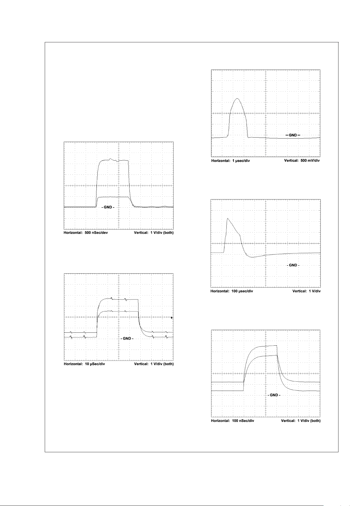
SYSTEM INTERFACE SIGNALS
The Horizontal and Vertical Blanking and the Clamping input
signals are important for proper functionality of the LM1238.
Both blanking inputs must be present for OSD synchronization. In addition, the Horizontal blanking input also assists in
setting the proper cathode black level, along with the Clamping pulse. The Vertical blanking input initiates a blanking
level at the LM1238 outputs which is programmable from 3
to 127 lines (we recommend at least 10). This can be optionally disabled so there is no vertical blanking.
20038754
FIGURE 2. Logic Horizontal Blanking
20038755
FIGURE 3. Logic Vertical Blanking
20038756
FIGURE 4. Deflection Horizonal Blanking
20038757
FIGURE 5. Deflection Vertical Blanking
20038758
FIGURE 6. Logic Clamp Pulse
LM1238
www.national.com 6
Page 7
Typical Performance
Characteristics
VCC= 5V, TA= 25˚C unless
otherwise specified (Continued)
Figure 2 and Figure 3 show the case where the Horizontal
and Vertical inputs are logic levels. Figure 2 shows the
smaller pin 24 voltage superimposed on the horizontal
blanking pulse input to the neck board with R
H
= 4.7K and
C
17
= 0.1µF. Note where the voltage at pin 24 is clamped to
about 1 volt when the pin is sinking current. Figure 3 shows
the smaller pin 1 voltage superimposed on the vertical blanking input to the neck board with C
4
jumpered and RV= 4.7K.
Figure 4 and Figure 5 show the case where the horizontal
and vertical inputs are from deflection. Figure 4 shows the
pin 24 voltage which is derived from a horizontal flyback
pulse of 35 volts peak to peak with R
H
= 8.2K and C
17
jumpered. Figure 5 shows the pin 1 voltage which is derived
from a vertical flyback pulse of 55 volts peak to peak with C
4
= 1500pF and RV= 120K.
Figure 6 shows the pin 23 clamp input voltage superimposed
on the neck board clamp logic input pulse. R
31
= 1K and
should be chosen to limit the pin 23 voltage to about 2.5V
peak to peak. This corresponds to the application circuit
given in Figure 9.
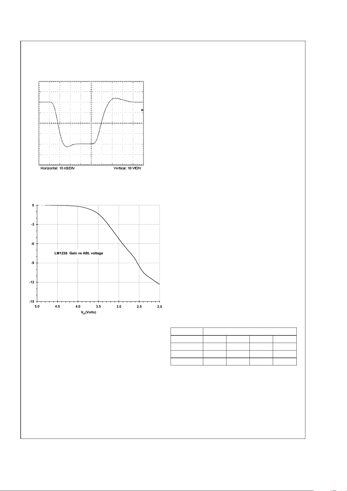
CATHODE RESPONSE
Figure 7 shows the response at the red cathode for the
application circuit in Figures 9, 10. The input video risetime is
1.5 nanoseconds. The resulting leading edge has a 10.1
nanosecond risetime and a 8% overshoot, while the trailing
edge has a 8.3 nanosecond risetime and a 2% overshoot
with an LM2469 driver.
ABL GAIN REDUCTION
The ABL function reduces the contrast level of the LM1238
as the voltage on pin 22 is lowered from V
CC
to around 2
volts. Figure 8 shows the amount of gain reduction as the
voltage is lowered from V
CC
(5.0V) to 2V. The gain reduction
is small until V
22
reaches the knee anound 3.7V, where the
slope increases. Many system designs will require about 3 to
5 dB of gain reduction in full beam limiting. Additional attenuation is possible, and can be used in special circumstances.
However, in this case, video performance such as video
linearity and tracking between channels will tend to depart
from normal specifications.
OSD PHASE LOCKED LOOP
Table 2 shows the recommended horizontal scan rate
ranges (in kHz) for each combination of PLL register setting,
0x081E [1:0], and the pixels per line register setting, 0x0802
[7:6]. While the OSD PLL may lock for other combinations,
the performance of the loop will be improved if these recommendations are followed. NR means the combination of PLL
and PPL is not recommended for any scan rate.
TABLE 2. OSD Register Recommendations
Pixels per Line
PLL Range 130 176 240 352
1 30-45 30-41 30-40 30-41
2 45-89 41-82 40-79 41-82
3 89-100 82-100 79-100 82-100
20038759
FIGURE 7. Red Cathode Response
20038760
FIGURE 8. ABL Gain Reduction Curve
LM1238
www.national.com7
Page 8
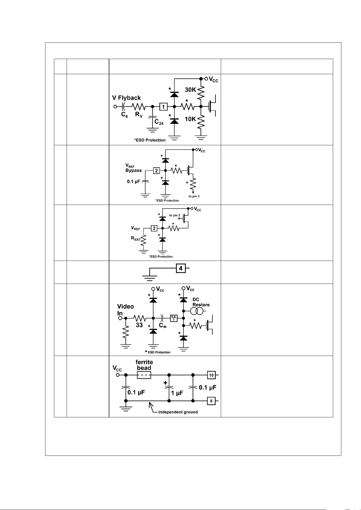
Pin Descriptions and Application Information
Pin
No.
Pin Name Schematic Description
1 V Flyback
Required for OSD synchronization and is also
used for vertical blanking of the video outputs.
The actual switching threshold is about 35% of
V
CC
. For logic level inputs C4can be a jumper,
but for flyback inputs, an AC coupled
differentiator is recommended, where R
V
is large
enough to prevent the voltage at pin 1 from
exceeding V
CC
or going below GND. C4should
be small enough to flatten the vertical rate ramp
at pin 1. C
24
may be needed to reduce noise.
2V
REF
Bypass Provides filtering for the internal voltage which
sets the internal bias current in conjunction with
R
EXT
. A minimum of 0.1 µF is recommended for
proper filtering. This capacitor should be placed
as close to pin 2 and the pin 4 ground return as
possible.
3V
REF
Current Set External resistor, 10k 1%, sets the internal bias
current level for optimum performance of the
LM1238. This resistor should be placed as close
to pin 3 and the pin 4 ground return as possible.
4 Analog Ground
This is the ground for the analog portions of the
LM1238 internal circuitry.
5
6
7
Blue Video In
Red Video In
Green Video In
These video inputs must be AC coupled with a
.0047 µF cap. Internal DC restoration is done at
these inputs. A series resistor of about 33Ω and
external ESD protection diodes should also be
used for protection from ESD damage.
8
10
PLL Ground
PLL V
CC
The ground pin should be connected to the rest
of the circuit ground by a short but independent
PCB trace to prevent contamination by
extraneous signals. The V
CC
pin should be
isolated from the rest of the V
CC
line by a ferrite
bead and bypassed to pin 8 with an electrolytic
capacitor and a high frequency ceramic.
LM1238
www.national.com 8
Page 9

Pin Descriptions and Application Information (Continued)
Pin
No.
Pin Name Schematic Description
9 PLL Filter Recommended topology and values are shown
to the left. It is recommended that both filter
branches be bypassed to the independent
ground as close to pin 8 as possible. Great care
should be taken to prevent external signals from
coupling into this filter from video, I
2
C, etc.
11 SDA
The I2C compatible data line. A pull-up resistor
of about 2 Kohms should be connected between
this pin and V
CC
. A resistor of at least 100Ω
should be connected in series with the data line
for additional ESD protection.
12 SCL
The I2C compatible clock line. A pull-up resistor
of about 2 kΩ should be connected between this
pin and V
CC
. A resistor of at least 100Ω should
be connected in series with the clock line for
additional ESD protection.
13
14
15
16
DAC 4 Output
DAC 2 Output
DAC 3 Output
DAC 1 Output
DAC outputs for cathode cut-off adjustments and
brightness control. DAC 4 can be set to change
the outputs of the other three DACs, acting as a
brightness control. The DAC values and the
special DAC 4 function are set through the I
2
C
compatible bus. A resistor of at least 100Ω
should be connected in series with these outputs
for additional ESD protection.
17
18
Ground
V
CC
Ground pin for the digital portion of the LM1238
circuitry, and power supply pin for both analog
and digital sections of the LM1238. Note the
recommended charge storage and high
frequency capacitors which should be as close
to pins 17 and 18 as possible.
19
20
21
Green Output
Red Output
Blue Output
These are the three video output pins. They are
intended to drive the LM246x family of cathode
drivers. Nominally, about 2V peak to peak will
produce 40V peak to peak of cathode drive.
LM1238
www.national.com9
Page 10

Pin Descriptions and Application Information (Continued)
Pin
No.
Pin Name Schematic Description
22 ABL The Automatic Beam Limiter input is biased to
the desired beam current limit by R
ABL
and V
BB
and normally keeps D
INT
forward biased. When
the current resupplying the CRT capacitance
(averaged by C
ABL
) exceeds this limit, then D
INT
begins to turn off and the voltage at pin 22
begins to drop. The LM1238 then lowers the
gain of the three video channels until the beam
current reaches an equilibrium value.
23 CLAMP
This pin accepts either TTL or CMOS logic
levels. The internal switching threshold is
approximately one-half of V
CC
. An external
series resistor, R
31
, of about 1k is recommended
to avoid overdriving the input devices. In any
event, R
EXT
must be large enough to prevent the
voltage at pin 23 from going higher than V
CC
or
below GND.
24 H Flyback
Proper operation requires current reversal. R
H
should be large enough to limit the peak current
at pin 24 to about +4 ma during blanking, and
−500 µA during scan. C
17
is usually needed for
logic level inputs and should be large enough to
make the time constant, R
HC17
significantly
larger than the horizontal period. R
34
and C8are
typically 300 ohms and 330 pf when the flyback
waveform has ringing and needs filtering. C
18
may be needed to filter extraneous noise and
can be up to 100 pF.
LM1238
www.national.com 10
Page 11

Schematic Diagram
20038716
FIGURE 9. LM123x-LM246x Demo Board Schematic
LM1238
www.national.com11
Page 12

Schematic Diagram
20038717
FIGURE 10. LM123x-LM246x Demo Board Schematic (continued)
LM1238
www.national.com 12
Page 13

PCB Layout
20038718
FIGURE 11. LM123x-LM246x Demo Board Layout
LM1238
www.national.com13
Page 14

OSD Operation
The LM1238 is designed to enable ultra-low cost OSD operation in monitors that usually use a simple button + LED
interface instead of OSD.
The basic screen is formed by a frame as shown in figure 12
below. The frame consists of a screen image with a bar
graph beneath the image and an index pointer on the right
hand side. This basic frame is common to all different views
of the OSD. The blank ’screen image’ of the screen in figure
12 is used to display one (or one set) of the available icons
which would correspond to the adjustment being carried out.
The available icons are shown in Figures 13 and 14. The 16
position index pointer is used to provide an indication of
which icon set of the 16 available is currently displayed. The
16 icon sets can be arranged in any order. The bar graph is
adjustable to 32 different lengths and can be used to indicate
where the adjustment level is in the available adjustment
range.
OSD MODES
Two modes of operation are available: alternating sequence
and fixed icon. In the alternating sequence mode, the display
will sequence through the three icons in the selected icon
set. For example, if the color temperature icon set (Icon set
15) is selected, the icon display will sequence from the 9300
icon (Screen 0) to the 6500 icon (Screen 1) to the 5000 icon
(Screen 2), then back to the 9300 icon (Screen 0). This
sequence will be continuously repeated under hardware
control. The rate of the sequence is controllable in increments of 8 frames of video by programming the lower 4 bits
of control register 0x0804 via the I2C interface. The display
is also capable of continuously displaying one of the three
icons in the set by programming bits 4 and 5 of control
register 0x0804.
OSD Constant Character Height Function
A constant height function is included in the LM1238 to
maintain a constant OSD height as the number of horizontal
image lines varies. Certain OSD character lines must be
repeated in order to maintain a constant height as a percentage of the vertical image size. The constant character height
function implements an approximation algorithm that determines which lines are repeated, and how many times each
line is repeated. This will maintain a relatively constant
height and position for the OSD window.
OSD SIZE AND POSITION
The size and position of the OSD is controlled by two registers. The available selections for horizontal size are 130,
176, 240, and 352 pixels per line. The horizontal position is
controllable in 64 steps of 8 pixels. The start point is referenced to the horizontal blank pulse. The available selections
for the vertical height of the OSD are 95, 130, 180, and 240
lines per field. The vertical position is adjustable in 64 increments of 8 OSD lines. The start point is referenced to the
vertical blank pulse.
20038761
FIGURE 12. Basic OSD Frame
LM1238
www.national.com 14
Page 15

OSD Operation (Continued)
20038763
FIGURE 13. The First 8 Icon Sets (0-7)
LM1238
www.national.com15
Page 16

OSD Operation (Continued)
20038762
FIGURE 14. Last 8 Icon Sets (8-15)
LM1238
www.national.com 16
Page 17

Microcontroller Interface
The microcontroller interfaces to the LM1238 preamp via the
I
2
C compatible interface. The protocol of the interface begins
with a Start Pulse followed by a byte comprised of a seven
bit Slave Device Address and a Read/Write bit. Since the
first byte is composed of both the address and the read/write
bit, the address of the LM1238 for writing is 0xBA
(10111010b) and the address for reading is 0xBB
(10111011b). The development software provided by National Semiconductor will automatically take care of the difference between the read and write addresses if the target
address under the communications tab is set to 0xBA. Fig-
ure 15 and Figure 16 show a write and read sequence on the
I
2
C compatible interface.
WRITE SEQUENCE
The write sequence begins with a start condition which
consists of the master pulling SDA low while SCL is held
high. The slave device address is next sent. The address
byte is made up of an address of seven bits (7-1) and the
read/write bit (0). Bit 0 is low to indicate a write operation.
Each byte that is sent is followed by an acknowledge. When
SCL is high the master will release the SDA line. The slave
must pull SDA low to acknowledge. The register to be written
to is next sent in two bytes, the least significant byte being
sent first. The master can then send the data, which consists
of one or more bytes. Each data byte is followed by an
acknowledge bit. If more than one data byte is sent the data
will increment to the next address location. See Figure 15.
READ SEQUENCE
Read sequences are comprised of two I
2
C compatible transfer sequences: The first is a write sequence that only transfers the two byte address to be accessed. The second is a
read sequence that starts at the address transferred in the
previous address only write access and increments to the
next address upon every data byte read. This is shown in
Figure 16. The write sequence consists of the Start Pulse,
the Slave Device Address, the Read/Write bit (a zero, indicating a write) and the Acknowledge bit; the next byte is the
least significant byte of the address to be accessed, followed
by its Acknowledge bit. This is then followed by a byte
containing the most significant address byte, followed by its
Acknowledge bit. Then a Stop bit indicates the end of the
address only write access. Next the read data access will be
performed beginning with the Start Pulse, the Slave Device
Address, the Read/Write bit ( a one, indicating a read) and
the Acknowledge bit. The next 8 bits will be the read data
driven out by the LM1238 preamp associated with the address indicated by the two address bytes. Subsequent read
data bytes will correspond to the next increment address
locations. Data should only be read from the LM1238 when
both OSD windows are disabled.
20038726
FIGURE 15. I2C Compatible Write Sequence
LM1238
www.national.com17
Page 18

Microcontroller Interface (Continued)
20038727
FIGURE 16. I2C Compatible Read Sequence
LM1238
www.national.com 18
Page 19

LM1238 Address Map
TABLE 3. I2C Address Space
Address Range R/W Description
0x0800h-0x0805h R/W OSD register set up data
0x0810h-0x081Fh R/W Preamp register set up data
Pre-Amp Interface I2C Registers
TABLE 4. LM1238 Pre-Amplifier Interface I2C Registers
Register Address Default D7 D6 D5 D4 D3 D2 D1 D0
BGAINCTRL 0x0810 0xE0h RSV BGAIN[6:0]
GGAINCTRL 0x0811 0xE0h RSV GGAIN[6:0]
RGAINCTRL 0x0812 0xE0h RSV RGAIN[6:0]
CONTRCTL 0x0813 0xE0h RSV CONTRAST[6:0]
DAC2CTRL 0x0814 0x80h DAC2[7:0]
DAC3CTRL 0x0815 0x80h DAC3[7:0]
DAC1CTRL 0x0816 0x80h DAC1[7:0]
DAC4CTRL 0x0817 0x80h DAC4[7:0]
DCF/OSD-Con/DC 0x0818 0x94h
*
RSV DCONFIG[1..0] OSD_CONT[1..0] DC_OFFSET[2..0]
GLOBALCTRL 0x0819 0x00h
*
D_ID[5:0] PS BV
CLMP/PLL/VBL/OOR 0x81E 0x16h
*
INT NV CLMP FRE OOR VBL PFR[1:0]
SRTSTCTRL 0x81F 0x00h
*
RSV RSV RSV RSV RSV RSV RSV SRST
TABLE 5. OSD Interface I
2
C Registers
Register Address Default D7 D6 D5 D4 D3 D2 D1 D0
BAR_CNTL 0x0800h 0x00h BAR[4:0] CNTL[2:0]
ICN_INDX 0x0801h 0x00h ICON[3:0] INDEX[2:0]
HORIZ 0x0802h 0xD0h PPL[1:0] HPOS[5:0]
VERT 0x0803h 0xCCh HT[1:0] VPOS[5:0]
ALT 0x0804h 0x04h RSV RSV ASO1 ASO0 ALT[3:0]
VERTBLNK 0x0805h 0x10h RSV VB[6:0]
Control Register Definitions
OSD INTERFACE REGISTERS
Bar Indicator and OSD Interface Control Register (I
2
C address 0x0800h)
Register Name (address): BAR_CNTL (0x0800h)
76543210
BAR4 BAR3 BAR2 BAR1 BAR0 CNTL2 CNTL1 CNTL0
Bits 2– 0 OSD Controls. These three bits turn on and off the OSD window and allow the up, down, left and right icons to be
highlighted in color 1 out of the 8 colors available.
Note that when the highlight bits are turned on, the control codes will be reset to 001b, after 32 vertical field periods.
Reading back the register more than 32 fields after a write to these bits will give 00 for the bits 1 and 2.
210
0 0 0 Turn off OSD
0 0 1 Turn on OSD and normal button colors
0 1 0 Turn on OSD and highlight up arrow for 32 vertical periods.
1 0 0 Turn on OSD and highlight down arrow for 32 vertical
periods.
0 1 1 Turn on OSD and highlight “+” for 32 vertical periods.
LM1238
www.national.com19
Page 20

Control Register Definitions (Continued)
210
1 1 1 Turn on OSD and highlight “−” for 32 vertical periods.
Bits 7– 3 Bar Indicator. These five bits determine the length of the bar indicator on a scale of 0–31. A value of 0 results in no
indicator. 31 results in a full scale indicator.
Icon Select and Index Position Register (I
2
C address 0x0801h)
Register Name (address): ICN_INDX (0x0801h)
76543210
ICN3 ICN2 INC1 INC0 INDX3 INDX2 INDX1 INDX0
Bits 3– 0 Index Pointer. These four bits determine the location of the pointer on a scale of 0–15. A value of 0 positions the pointer
at the top. A value of 15 positions it at the bottom.
Bits 7– 4 Icon Select. These four bits determine the icon set (0 through 15) that is displayed.
Horiz. Pixels Per Line and OSD Horiz. Position Register (I
2
C address 0x0802h)
Register Name (address): HORIZ (0x0802h)
76543210
PPL1 PPL0 HPOS5 HPOS4 HPOS3 HPOS2 HPOS1 HPOS0
Bits 5– 0 Horizontal Position. These six bits set the position of the image relative to the blanking pulse in increments of 8 pixels
(i.e., one character cell).
Bits 7– 6 Pixels Per Line. These two bits set the horizontal size of the image, in pixels per line.
TABLE 6. Pixels Per Line vs Register Value
Pixel Per Line
Register Value
Pixels Per Line
00 130
01 176
10 240
11 352
OSD Vertical Height and Vertical Position Register (I
2
C address 0x0803h)
Register Name (address): VERT (0x0803h)
76543210
HT1 HT0 VPOS5 VPOS4 VPOS3 VPOS2 VPOS1 VPOS0
Bits 5– 0 Vertical Position. This six bit value sets the position of the image relative to the vertical blank pulse in increments of 8
OSD lines (one character cell height).
Bits 7– 6 Vertical Height. This two bit value sets the nominal height of the OSD by controlling the average number of OSD lines
per frame.
TABLE 7. OSD Lines Per Field vs Vertical Height Register
Vertical Height
Register Value
OSD Lines Per Field
00 95
01 130
10 180
11 260
LM1238
www.national.com 20
Page 21

Control Register Definitions (Continued)
Icon Alternate Period Control Register (I
2
C address 0x0804h)
Register Name (address): ALT (0x0804h)
76543210
RSV RSV ASO1 ASO0 ALT3 ALT2 ALT1 ALT0
Bits 3– 0 Icon Alternate Period. These four bits set the period at which the icon will switch between images, in increments of eight
vertical fields.
Bits 5– 4 Alternate Sequence Override. These two bits enable the automatic alternating sequence of icons, or allow the icon to
be set to one of the three alternative screens.
TABLE 8. Alternating Icon Sequence Override
Sequence Override
Register Value
Effect
00 Automatic Alternating Sequence
01 Set for Icon Screen 0
10 Set for Icon Screen 1
11 Set for Icon Screen 2
Bits 7– 6 Reserved.
Vertical Blank Duration Control Register (I
2
C address 0x0805h)
Register Name (address): VERTBLNK (0x0805h)
76543210
RSV VB6 VB5 VB4 VB3 VB2 VB1 VB0
Bits 6– 0 Vertical Blank Duration. These seven bits set the duration of the VBLANK signal in numbers of horizontal scans.
Bit 7 Reserved.
PRE-AMPLIFIER INTERFACE REGISTERS
Blue Channel Gain Control Register (I
2
C address 0x0810h)
Register Name (address): BGAINCTRL (0x0810h)
76543210
RSV BG BG BG BG BG BG BG
Bits 6– 0 Blue Channel Gain Control. These seven bits determine the gain for the Blue Channel.
Bit 7 Reserved.
Green Channel Gain Control Register (I
2
C address 0x0811h)
Register Name (address): GGAINCTRL1 (0x0811h)
76543210
RSV GG GG GG GG GG GG GG
Bits 6– 0 Green Channel Gain Control. These seven bits determine the gain for the Green Channel.
Bit 7 Reserved.
Red Channel Gain Control Register (I
2
C address 0x0812h)
Register Name (address): RGAINCTRL1 (0x0812h)
76543210
RSV RG RG RG RG RG RG RG
Bits 6– 0 Red Channel Gain Control. These seven bits determine the gain for the Red Channel.
Bit 7 Reserved.
LM1238
www.national.com21
Page 22

Control Register Definitions (Continued)
Contrast Control Register (I
2
C address 0x0813h)
Register Name (address): CONTRCTRL (0x0813h)
76543210
RSV CO CG CG CG CG CG CG
Bits 6– 0 Contrast Gain Control. These seven bits determine the overall gain of all the three channels.
Bit 7 Reserved.
DAC2 Register (I
2
C address 0x0814h)
Register Name (address): DAC2CTRL (0x0814h)
76543210
D2–7 D2–6 D2–5 D2–4 D2– 3 D2– 2 D2–1 D2– 0
Bits 7– 0 These bits determine the output voltage of DAC2.
DAC3 Register (I
2
C address 0x0815h)
Register Name (address): DAC3CTRL (0x0815h)
76543210
D3–7 D3–6 D3–5 D3–4 D3– 3 D3– 2 D3–1 D3– 0
Bits 7– 0 These bits determine the output voltage of DAC3.
DAC1 Register (I
2
C address 0x0816h)
Register Name (address): DAC1CTRL (0x0816h)
76543210
D1–7 D1–6 D1–5 D1–4 D1– 3 D1– 2 D1–1 D1– 0
Bits 7– 0 These bits determine the output voltage of DAC1.
DAC4 Register (I
2
C address 0x0817h)
Register Name (address): DAC4CTRL (0x0817h)
76543210
D4–7 D4–6 D4–5 D4–4 D4– 3 D4– 2 D4–1 D4– 0
Bits 7– 0 These bits determine the output voltage of DAC4.
DCoffset/OSD Contrast/DAC Configuration Control Register (I
2
C address 0x0818h)
Register Name (address): DCF/OSD_CON/DC (0x0818h)
76543210
RSV DCF1 DCF0 OSD OSD DC2 DC1 DC0
Bits 2– 0 DC Offset Control. These three bits determine the active video DC offset to all three channels.
Bits 4– 3 OSD Contrast Control. These two bits determine the contrast level of the OSD information.
Bit 5 DAC1–3 Configuration. When this bit is a 0 (default) the DAC outputs of DAC1–3 are full scale (0.5V–4.5V). When this
bit is 1, the range of DAC1– 3 are halved (0.5V–2.5V).
Bit 6 DAC4 Configuration. When this bit is a 0 (default), the DAC4 output is not mixed with the other DAC outputs. When the
bit is one, 50% of the DAC4 output is added to DAC1– 3.
Bit 7 Reserved.
LM1238
www.national.com 22
Page 23

Control Register Definitions (Continued)
Global Video Control Register (I
2
C address 0x0819h)
Register Name (address): GLOBALCTRL (0x0819h)
76543210
D_ID5 D_ID4 D_ID3 D_ID2 D_ID1 D_ID0 PS BV
Bit 0 Blank Video. When this bit is a one, blank the video output. When this bit is a zero allow normal video out. This register
bit is OR’d with the other video blank signals, both active and static, and sent to the preamplifier as BLANK_OUT.
Bit 1 Power Save. When this bit is a one, shut down the analog circuits to support sleep mode. When this bit is a zero
(default) enable the analog circuits for normal operation. This register bit is fed to the preamplifier interface as
PWR_SAVE so that the amplifier can be put in to low power sleep mode. It is also OR’d with the blanking signals to
blank the video.
Bits 7– 2 Die ID. These bits are read only masked so that they can be assigned a value to differentiate between masked dies and
die revisions.
PLL Range Register (I
2
C address 0x081Eh)
Register Name (address): CLMP/PLL/VBL/OOR (0x081Eh)
76543210
INT BIS CLMP FRE OOR VBL PFR1 PFR0
Bits 1– 0 PLL Frequency Range Control. These bits assist the PLL in locking to the desired pixel frequency. They are set based
upon the nominal desired horizontal frequency range as per the PLL section. These bits, PFR0,1 are presented at the
PLL interface as the signals ‘Free_run_freq0’, and ‘Free_run_freq1’.
Bit 2 Vertical Blank Disable. When this bit is set to 0, the internally generated vertical blanking pulse is OR’d with the
horizontal blank pulse internal to the logic core, to blank the video during retrace. When this bit is set to 1 (default) the
internal vertical blanking is disabled.
Bit 3 OSD Override. When this bit is 0 (default) normal video operation is assumed. When this bit is 1, the OSD select is
overridden, and OSD only is selected, preventing normal video from being displayed (used for ‘out-of-range’ condition).
Bit 4 Free Run Enable. When this bit is set to 0 (default), the PLL will be supplied with the H flyback synchronization pulse.
When set to 1, the H flyback pulse will be gated off.
Bit 5 Clamp Polarity. Determines the polarity of the clamp signal used by the LM1238. When this bit is 0 (default) the LM1238
requires a positive clamp signal. When this bit is 1, the LM1238 requires a negative going clamp signal.
Bit 6 Burn-in Screen Enable (BIS). When this bit is a ’1’, the burn-in screen is active and input video will be ignored. When
this bit is a ’0’ (default), the burn-in screen is disabled.
Bit 7 Interface. When this bit is set to 1, the jitter reduction circuit is set to alternate the phase every alternate field. When it
is set to 0 (default), normal progressive scan is assumed.
Software Reset and Test Control Register (I
2
C address 0x081Fh)
Register Name (address): SRTSTCTRL (0x081Fh)
76543210
RSV RSV RSV RSV RSV RSV RSV SRST
Bit 0 Software Reset. Setting this bit causes a software reset. All registers (except this one) are loaded with their default
values. All operations currently in progress are aborted (except for I
2
C transactions). This bit automatically clears itself
when the reset has been completed.
Bits 1– 7 Reserved.
LM1238
www.national.com23
Page 24

Physical Dimensions inches (millimeters) unless otherwise noted
LIFE SUPPORT POLICY
NATIONAL’S PRODUCTS ARE NOT AUTHORIZED FOR USE AS CRITICAL COMPONENTS IN LIFE SUPPORT
DEVICES OR SYSTEMS WITHOUT THE EXPRESS WRITTEN APPROVAL OF THE PRESIDENT AND GENERAL
COUNSEL OF NATIONAL SEMICONDUCTOR CORPORATION. As used herein:
1. Life support devices or systems are devices or
systems which, (a) are intended for surgical implant
into the body, or (b) support or sustain life, and
whose failure to perform when properly used in
accordance with instructions for use provided in the
labeling, can be reasonably expected to result in a
significant injury to the user.
2. A critical component is any component of a life
support device or system whose failure to perform
can be reasonably expected to cause the failure of
the life support device or system, or to affect its
safety or effectiveness.
National Semiconductor
Americas Customer
Support Center
Email: new.feedback@nsc.com
Tel: 1-800-272-9959
National Semiconductor
Europe Customer Support Center
Fax: +49 (0) 180-530 85 86
Email: europe.support@nsc.com
Deutsch Tel: +49 (0) 69 9508 6208
English Tel: +44 (0) 870 24 0 2171
Français Tel: +33 (0) 1 41 91 8790
National Semiconductor
Asia Pacific Customer
Support Center
Email: ap.support@nsc.com
National Semiconductor
Japan Customer Support Center
Fax: 81-3-5639-7507
Email: jpn.feedback@nsc.com
Tel: 81-3-5639-7560
www.national.com
LM1238 110 MHz I
2
C Compatible RGB Preamplifier with Internal Simple OSD Generator 4 DACs
National does not assume any responsibility for use of any circuitry described, no circuit patent licenses are implied and National reserves the right at any time without notice to change said circuitry and specifications.
 Loading...