

Page 1
LM122/LM322/LM3905 Precision Timers
General Description
The LM122 series are precision timers that offer great versatility with high accuracy. They operate with unregulated
supplies from 4.5V to 40V while maintaining constant timing
periods from microseconds to hours. Internal logic and regulator circuits complement the basic timing function
enabling the LM122 series to operate in many different applications with a minimum of external components.
The output of the timer is a floating transistor with built in
current limiting. It can drive either ground referred or supply
referred loads up to 40V and 50 mA. The floating nature of
this output makes it ideal for interfacing, lamp or relay driving, and signal conditioning where an open collector or emitter is required. A ‘‘logic reverse’’ circuit can be programmed
by the user to make the output transistor either ‘‘on’’ or
‘‘off’’ during the timing period.
The trigger input to the LM122 series has a threshold of
1.6V independent of supply voltage, but it is fully protected
against inputs as high as
g
40VÐeven when using a 5V
supply. The circuitry reacts only to the rising edge of the
trigger signal, and is immune to any trigger voltage during
the timing periods.
An internal 3.15V regulator is included in the timer to reject
supply voltage changes and to provide the user with a convenient reference for applications other than a basic timer.
External loads up to 5 mA can be driven by the regulator. An
internal 2V divider between the reference and ground sets
the timing period to 1 RC. The timing period can be voltage
controlled by driving this divider with an external source
through the V
achieved.
pin. Timing ratios of 50:1 can be easily
ADJ
The comparator used in the LM122 utilizes high gain PNP
input transistors to achieve 300 pA typical input bias current
over a common mode range of 0V to 3V. A boost terminal
allows the user to increase comparator operating current for
timing periods less than 1 ms. This lets the timer operate
over a 3 ms to multi-hour timing range with excellent repeatability.
The LM122 operates over a temperature range of
a
125§C. An electrically identical LM322 is specified from
0
Ctoa70§C. The LM3905 is identical to the LM122 series
§
except that the boost and V
able, limiting minimum timing period to 1 ms.
Features
Y
Immune to changes in trigger voltage during timing
interval
Y
Timing periods from microseconds to hours
Y
Internal logic reversal
Y
Immune to power supply ripple during the timing
interval
Y
Operates from 4.5V to 40V supplies
Y
Input protected tog40V
Y
Floating transistor output with internal current limiting
Y
Internal regulated reference
Y
Timing period can be voltage controlled
Y
TTL compatible input and output
February 1995
pin options are not avail-
ADJ
b
55§Cto
LM122/LM322/LM3905 Precision Timers
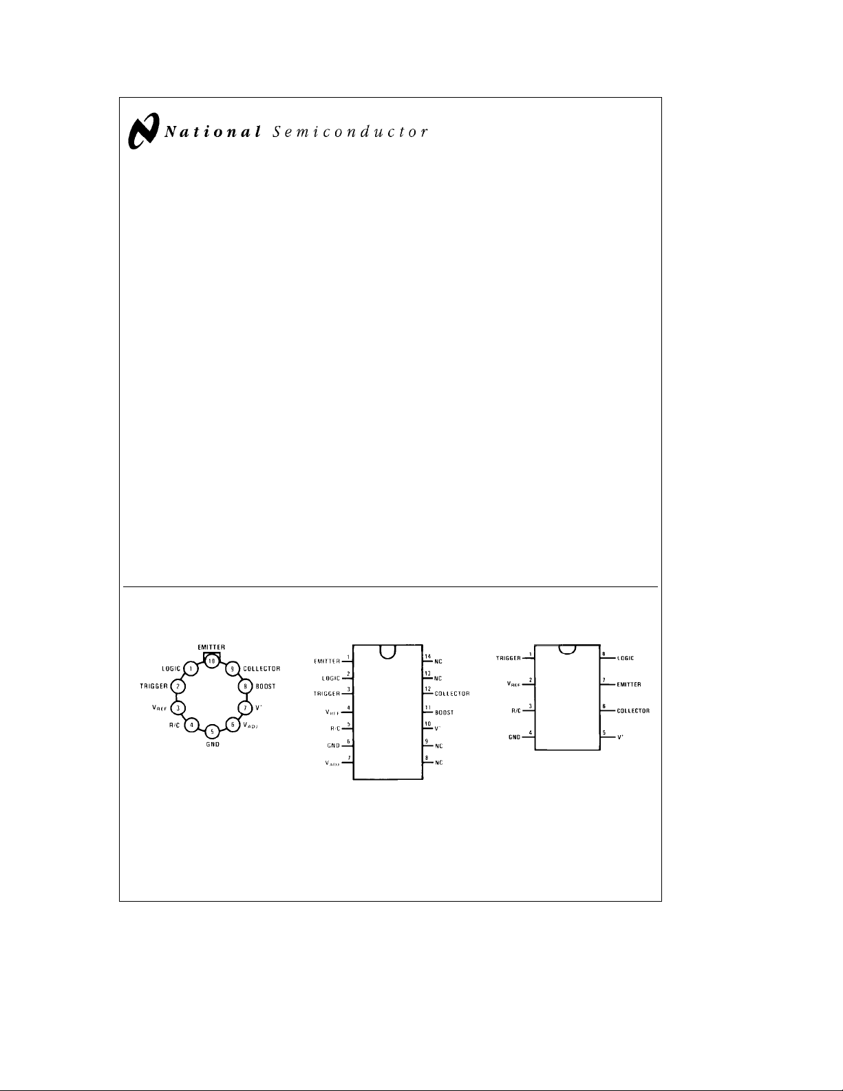
Connection Diagrams
Metal Can Package
TL/H/7768– 6
Dual-In-Line Package
Top View
Order Number LM122H
See NS Package Number H10C
Top View
TL/H/7768– 7
Order Number LM322N
See NS Package Number N14A
C
1995 National Semiconductor Corporation RRD-B30M115/Printed in U. S. A.
TL/H/7768
Dual-In-Line Package
TL/H/7768– 8
Top View
Order Number LM3905N
See NS Package Number N08E
Page 2
Absolute Maximum Ratings
If Military/Aerospace specified devices are required,
please contact the National Semiconductor Sales
Office/Distributors for availability and specifications.
Power Dissipation 500 mW
a
V
Voltage 40V
Collector Output Voltage 40V
Current 5 mA
V
REF
Trigger Voltage
V
Voltage (Forced) 5V
ADJ
g
40V
Logic Reverse Voltage 5.5V
Output Short Circuit Duration (Note 1)
Lead Temperature
(Soldering, 10 sec.) 260
Operating Temperature Range
LM122
LM322 0
LM3905 0
b
55§CsT
CsT
§
CsT
§
s
a
125§C
A
s
a
70§C
A
s
a
70§C
A
§
Electrical Characteristics (Note 2)
Parameter Conditions
a
Timing Ratio T
Comparator Input T
Current Boost Tied to V
Trigger Voltage T
Trigger Current T
Supply Current T
Timing Ratio 4.5VsV
e
25§C, 4.5VsV
A
Boost Tied to V
e
25§C, 4.5VsV
A
e
25§C, 4.5VsV
A
e
25§C, V
A
t
25§C, 4.5VsV
A
a
s
Boost Tied to V
a
Comparator Input 4.5VsV
s
TRIG
s
a
a
40V 0.62 0.644 0.61 0.654 0.61 0.654
a
40V 0.626 0.632 0.638 0.620 0.632 0.644 0.620 0.632 0.644
, (Note 3) 0.620 0.632 0.644 0.620 0.632 0.644
a
s
40V 0.3 1.0 0.3 1.5 0.5 1.5 nA
a
s
40V 1.2 1.6 2 1.2 1.6 2 1.2 1.6 2 V
e
2V 25 25 25 mA
a
s
40V 2.5 4 2.5 4.5 2.5 4.5 mA
40V
Current Boost Tied to Va, (Note 4) 100 150 nA
a
Trigger Voltage 4.5VsV
Trigger Current V
Output Leakage V
Current
Capacitor Saturation R
Voltage R
TRIG
CE
t
t
s
40V 0.8 2.5 0.8 2.5 0.8 2.5 V
e
2.5V 200 200 200 mA
e
40V
t
1MX 2.5 2.5 2.5 mV
e
10 kX 25 25 25 mV
Reset Resistance 150 150 150 X
Reference Voltage T
Reference Regulation 0sI
Collector Saturation I
Voltage I
Emitter Saturation T
Voltage T
e
25§C 3 3.15 3.3 3 3.15 3.3 3 3.15 3.3 V
A
s
3mA 2050 2050 2050mV
OUT
a
s
4.5V
L
L
A
A
s
V
40V 6 25 6 25 6 25 mV
e
8 mA 0.25 0.4 0.25 0.4 0.25 0.4 V
e
50 mA 0.7 1.4 0.7 1.4 0.7 1.4 V
e
e
25§C, I
25§C, I
e
3 mA 1.8 2.2 1.8 2.2 1.8 2.2 V
L
e
50 mA 2.1 3 2.1 3 2.1 3 V
L
Average Temperature
Coefficient of Timing 0.003 0.003 0.003 %/
Ratio
Minimum Trigger Width V
Note 1: Continuous output shorts are not allowed. Short circuit duration at ambient temperatures up to 40§C may be calculated from te120/VCEseconds, where
is the collector to emitter voltage across the output transistor during the short.
V
CE
Note 2: These specifications apply for T
Note 3: Output pulse width can be calculated from the following equation: t
saturation voltage. This reduces to t
Note 4: Sign reversal may occur at high temperatures (
Note 5: Refer to RETS122X drawing of military LM122H version for specifications.
e
3V 0.25 0.25 0.25 ms
TRIG
s
s
T
T
AMIN
e
(Rt)(Ct) for all but the most critical applications.
unless otherwise noted.
A
AMAX
l
100§C) where comparator input current is predominately leakage. See typcial curves.
LM122 LM322 LM3905
Min Typ Max Min Typ Max Min Typ Max
30 100 30 100 nA
0.62 0.644 0.61 0.654
b
55
b
22
b
2.5 2.5 nA
155mA
e
(Rt)(Ct)[1b2(0.632br)bVC/V
) where r is timing ratio and VCis capacitor
REF
Units
C
C
§
2
Page 3
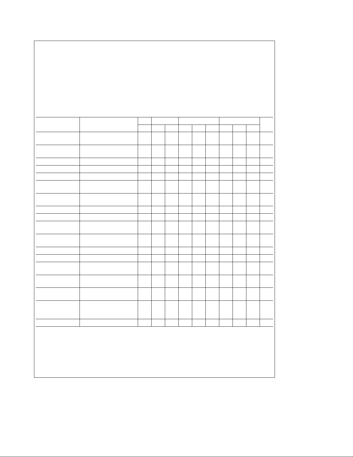
Typical Performance Characteristics
Comparator Bias Current Comparator Bias Current (LM122/LM322)
Supply Current Trigger Input Characteristics Trigger Threshold
Comparator Bias Current
TL/H/7768– 3
Output Transistor Saturation
Characteristics at Low Currents
Reference Regulation Reference Regulation Suggested Timing Components
Short Output Pulse
(LM122/LM322)
Collector Output Saturation
Characteristics at High Current
Short Output Pulse
(LM122/LM322)
Timing Error Due to
Comparator Bias Current
Logic Pin Characteristics
TL/H/7768– 4
3
Page 4
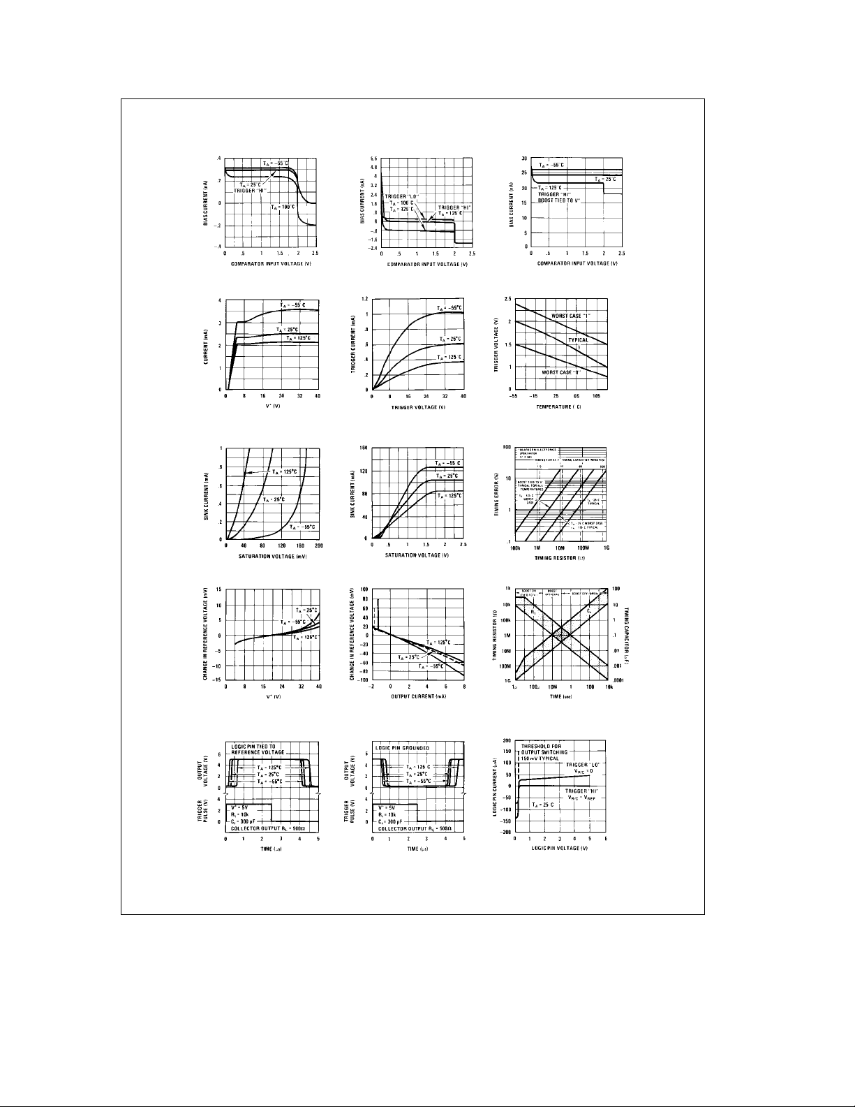
Schematic Diagram
TL/H/7768– 5
4
Page 5
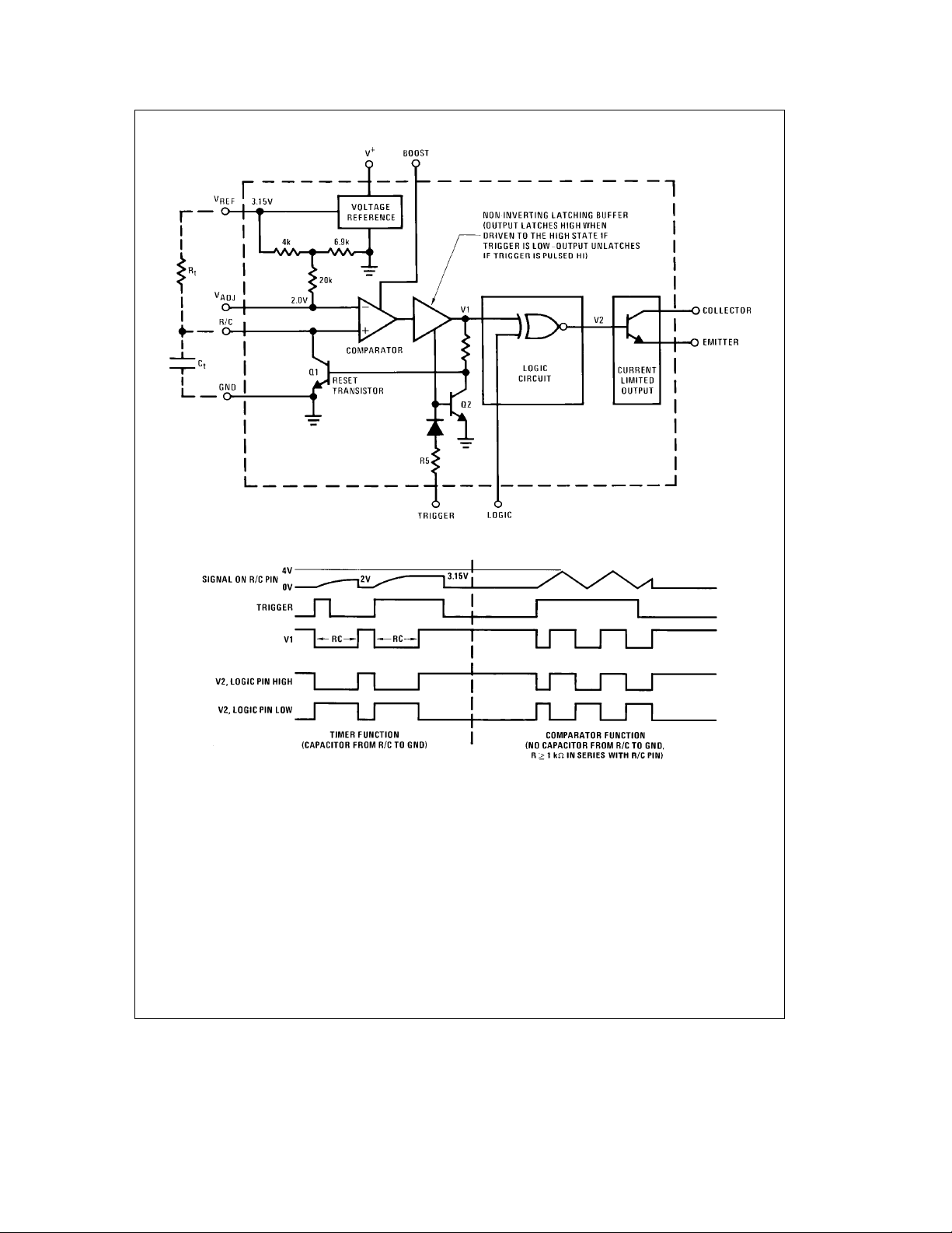
Functional Diagram
Timing Diagram
TL/H/7768– 9
Pin Function Description
One of the main features of the LM122 is its great versatility.
Since this device is unique, a description of the functions
and limitations of each pin is in order. This will make it much
easier to follow the discussion of the various applications
presented in this note.
a
V
is the positive supply terminal of the LM122. When using a single supply, this terminal may be driven by any voltage between 4.5V and 40V. The effect of supply variations
on timing period is less than 0.005%/V, so supplies with
high ripple content may be used without causing pulse width
changes. Supply bypassing on V
but may be necessary when driving highly reactive loads.
a
is not generally needed
Quiescent current drawn from the V
2.5 mA, independent of the supply voltage. Of course, additional current will be drawn if the reference is externally
loaded.
The V
enced to the ground pin. Up to 5.0 mA can be drawn from
this pin for driving external networks. In most applications
the timing resistor is tied to V
situations where a more linear charging current is required.
The regulated voltage is very useful in applications where
the LM122 is not used as a timer; such as switching regulators, variable reference comparators, and temperature con-
5
pin is the output of a 3.15V series regulator refer-
REF
a
terminal is typically
, but it need not be in
REF
TL/H/7768– 10
Page 6

Pin Function Description (Continued)
trollers. Typical temperature drift of the reference is less
than 0.01%/
The trigger terminal is used to start a timing cycle (see
functional diagram). Initially, Q1 is saturated, C
charged and the latching buffer output (V1) is latched high.
A trigger pulse unlatches the buffer, V1 goes low and turns
Q1 off. The timing capacitor C
will begin to charge. When the voltage at the R/C terminal
reaches the 2.0V threshold of the comparator, the comparator toggles, latching the buffer output (V1) in the high state.
This turns on Q1, discharges the capacitor C
is ready to begin again.
If the trigger is held high as the timing period ends, the
comparator will toggle and V1 will go high exactly as before.
However, V1 will not be latched and the capacitor will not
discharge until the trigger again goes low. When the trigger
goes low, V1 remains high but is now latched.
Trigger threshold is typically 1.6V at 25
perature dependence of
the trigger source is typically 20 mA at threshold, rising to
600 mA at 30V, then leveling off due to FET action of the
series resistor, R5. For negative input trigger voltages, the
only current drawn is leakage in the nA region. The trigger
can be driven from supplies as high as
device supply voltage is only 5V.
The R/C pin is tied to the non-inverting side of the comparator and to the collector of Q1. Timing ends when the voltage
on this pin reaches 2.0V (1 RC time constant referenced to
the 3.15V regulator). Q1 turns on only if the trigger voltage
has dropped below threshold. In comparator or regulator
applications of the timer, the trigger is held permanently
high and the R/C pin acts just like the input to an ordinary
comparator. The maximum voltages which can be applied to
this pin are
typically 300 pA when the voltage is negative with respect to
the V
leakage levels. In the boosted mode, input current is typically 30 nA. Gain of the comparator is very high, 200,000 or
more, depending on the state of the logic reverse pin and
the connection of the output transistor.
The ground pin of the LM122 need not necessarily be tied
to system ground. It can be connected to any positive or
negative voltage as long as the supply is negative with respect to the V
for the input trigger if the trigger voltage is referred to system ground. This can be done by capacitive coupling or by
actual resistive or active level shifting. One point must be
kept in mind; the emitter output must not be held above the
ground terminal with a low source impedance. This could
occur, for instance, if the emitter were grounded when the
ground pin of the LM122 was tied to a negative supply.
The terminal labled V
tor and to a voltage divider between V
divider voltage is set at 63.2% of V
groundÐexactly one RC time constant. The impedance of
the divider is increased to about 30k with a series resistor to
C.
§
connected from R/C to GND
t
and the cycle
t
C and has a tem-
b
5.0 mV/§C. Current drawn from
a
5.5V andb0.7V. Current from the R/C pin is
terminal. For higher voltages, the current drops to
ADJ
a
terminal. Level shifting may be necessary
is tied to one side of the compara-
ADJ
§
g
40V, even when
and ground. The
REF
with respect to
REF
is dis-
t
present a minimum load on external signals tied to V
This resistor is a pinched type with a typical variation in
nominal value of
b
50%,a100% and a TC of 0.7%/§C. For
this reason, external signals (typically a pot between V
and ground) connected to V
sistance as low as possible. For small changes in V
should have a source re-
ADJ
to several kX is all right, but for large variations, 250X or
ADJ
ADJ
REF
,up
less should be maintained. This can be accomplished with a
1k pot, since the maximum impedance from the wiper is
250X. If a voltage is forced on V
voltage should be limited to
limited to
g
1.0 mA. This includes capacitively coupled sig-
from a hard source,
ADJ
b
0.5, anda5.0V, or current
nals because even small values of capacitors contain
enough energy to degrade the input stage if the capacitor is
driven with a large, fast slewing signal. The V
used to abort the timing cycle. Grounding this pin during the
pin may be
ADJ
timing period causes the timer to react just as if the capacitor voltage had reached its normal RC trigger point; the
capacitor discharges and the output charges state. An exception to this occurs if the trigger pin is held high, when the
V
pin is grounded. In this case, the output changes
ADJ
state, but the capacitor does not discharge.
If the trigger drops while V
will occur immediately and the cycle will be over. If the trigger is still high when V
may not change state, depending on the voltage across the
is being held low, discharge
ADJ
is released, the output may or
ADJ
timing capacitor. For voltages below 2.0V across the timing
capacitor, the output will change state immediately, then
once more as the voltage rises past 2.0V. For voltages
above 2.0V, no change will occur in the output. This pin is
not available on the LM2905/LM3905.
In noisy environments or in comparator-type applications, a
bypass capacitor on the V
eliminate spurious outputs because it is high impedance
terminal may be needed to
ADJ
point. The size of the cap will depend on the frequency and
energy content of the noise. A 0.1 mF will generally suffice
for spike suppression, but several mF may be used if the
timer is subjected to high level 60 Hz EMI.
The emitter and the collector outputs of the timer can be
treated just as if they were an ordinary transistor with 40V
minimum collector-emitter breakdown voltage. Normally, the
emitter is tied to the ground pin and the signal is taken
from the collector,orthecollector is tied to V
a
and the
signal is taken from the emitter. Variations on these basic
connections are possible. The collector can be tied to any
positive voltage up to 40V when the signal is taken from the
emitter. However, the emitter will not be pulled higher than
the supply voltage on the V
to a voltage less than the V
a
pin. Connecting the collector
a
voltage is allowed. The emit-
ter should not be connected to a low impedance load other
than that to which the ground pin is tied. The transistor has
built-in current limiting with a typical knee current of 120 mA.
Temporary short circuits are allowed; even with collector-
emitter voltages up to 40V. The power x time product, however, must not exceed 15 watt-seconds for power levels
above the maximum rating of the package. A short to 30V,
.
6
Page 7

Pin Function Description (Continued)
for instance, cannot be held for more than 4 seconds.
These levels are based on 40
perature. When driving inductive loads, always use a clamp
diode to protect the transistor from inductive kick-back.
A boost pin is provided on the LM122 to increase the speed
of the internal comparator. The comparator is normally operated at low current levels for lowest possible input current.
For timing periods less than 1 ms, where low input current is
not needed, comparator operating current can be increased
several orders of magnitude. Shorting the boost terminal to
a
V
increases the emitter current of the vertical PNP drivers
in the differential stage from 25 nA to 5 mA. This pin is not
available on the LM3905.
With the timer in the unboosted state, timing periods are
accurate down to about 1 ms. In the boosted mode, loss of
accuracy due to comparator speed is only about 800 ns, so
timing periods of several microseconds can be used. The
800 ns error is relatively insensitive to temperature, so temperature coefficient of pulse width is still good.
The Logic pin is used to reverse the signal appearing at the
output transistor. An open or ‘‘high’’ condition on the logic
pin programs the output transistor to be ‘‘off’’ during the
timing period and ‘‘on’’ all other times. Grounding the logic
pin reverses the sequence to make the transistor ‘‘on’’ during the timing period. Threshold for the logic pin is typically
100 mV with 150 mA flowing out of the terminal. If an active
drive to the logic pin is desired, a saturated transistor drive
is recommended, either with a discrete transistor or the
open collector output of integrated logic. A maximum V
of 25 mV at 200 mA is required. Minimum and maximum
voltages that may appear on the logic pin are 0 and
respectively.
C maximum initial chip tem-
§
SAT
a
5.0,
FIGURE 1. Basic Timer-Collector
TL/H/7768– 11
Output and Timing Chart
TL/H/7768– 12
FIGURE 2. Basic Timer-Emitter Output and Timing Chart
Typical Applications
Basic Timers
Figure 1
is a basic timer using the collector output. Rtand C
set the time interval with RLas the load. During the timing
interval the output may be either high or low depending on
the connection of the logic pin. Timing waveforms are
shown in the sketch along side
ger pulse may be either shorter or longer than the output
pulse width.
Figure 2
is again a basic timer, but with the output taken
from the emitter of the output transistor. As with the collector output, either a high or low condition may be obtained
during the timing period.
Simulating a Thermal Delay Relay
Figure 3
is an application where the LM122 is used to simulate a thermal delay relay which prevents power from being
applied to other circuitry until the supply has been on for
some time. The relay remains de-energized for R
onds after V
until V
the relay is energized as soon as V
is applied, then closes and stays energized
CC
is turned off.
CC
Figure 4
onds later, the relay is de-energized and stays off until the
V
supply is recycled.
CC
Figure 1
. Note that the trig-
sec-
tCt
is a similar circuit except that
is applied. RtCtsec-
CC
t
FIGURE 3. Time Out on Power Up
(Relay Energized R
a
5V Supply Driving 28V Relay
Figure 5
shows the timer interfacing 5V logic to a high volt-
age relay. Although the V
a
28V supply, this may be an unnecessary waste of power
Seconds after VCCis Applied)
tCt
a
terminal could be tied to the
in the IC or require extra wiring if the LM122 is on a logic
card. In either case, the threshold for the trigger is 1.6V.
7
TL/H/7768– 13
Page 8

Typical Applications (Continued)
mined by the time required to discharge C
nal discharge transistor. A conservative value for C
chosen from the graph included with
cies below 1 kHz, the frequency error introduced by C
few tenths of one percent or less for R
through the inter-
t
Figure 20
t
500k.
t
f
. For frequen-
*See Chart
can be
is a
f
FIGURE 4. Time Out on Power Up (Relay Energized
TL/H/7768– 14
Until
RtCtSeconds After VCCis Applied)
FIGURE 5. 5V Logic Supply Driving 28V Relay
TL/H/7768– 15
30V Supply Interfacing with 5V Logic
Figure 6
indicates the ability of the timer to interface to digital logic when operating off a high supply voltage. V
swings betweena5V and ground with a minimum fanout of
OUT
5 for medium speed TTL. If the logic is sensitive to rise/fall
time of the trailing edge of the output pulse, the trigger pin
should be low at that time.
TL/H/7768– 17
TL/H/7768– 18
FIGURE 7. Oscillator
One Hour Timer with Reset and Manual Cycle End
Figure 8
shows the LM122 connected as a one hour timer
with manual controls for start, reset, and cycle end. S1
starts timing, but has no effect after timing has started. S2 is
a center off switch which can either end the cycle prematurely with the appropriate change in output state and discharging of C
change in output. In the latter case, a new timing period
, or cause Ctto be reset to 0V without a
t
starts as soon as S2 is released.
FIGURE 6. 30V Supply Interfacing with 5V Logic
TL/H/7768– 16
Astable Operation
The LM122 can be made into a self-starting oscillator by
feeding the output back to the trigger input through a capacitor as shown in
R1)(Ct). The output is a narrow negative pulse whose width
is approximately 2R
should be as small as possible. The minimum value is deter-
Figure 7
. Operating frequency is 1/(R
. For optimum frequency stability, C
2Cf
t
*Dearborn
Electronics
LP9A1A476K
Polycarbonate
a
f
FIGURE 8. One Hour Timer with Reset
and Manual Cycle End
TL/H/7768– 19
8
Page 9

Typical Applications (Continued)
The average charging current through R
some attention must be paid to parts layout to prevent stray
leakage paths. The suggested timing capacitor has a typical
self time constant of 300 hours and a guaranteed minimum
of 25 hours at
a
25§C. Other capacitor types may be used if
sufficient data is available on their leakage characteristics.
Two Terminal Time Delay Switch
The LM122 can be used as a two terminal time delay switch
if an ‘‘on’’ voltage drop of 2V to 3V can be tolerated. In
Figure 9
, the timer is used to drive a relay ‘‘on’’ R
seconds after application of power. ‘‘Off’’ current of the
switch is 4 mA maximum, and ‘‘on’’ current can be as high
as 50 mA.
Zero Power Dissipation Between Timing Intervals
In some applications it is desirable to reduce supply current
drain to zero between timing cycles. In
accomplished by using an external PNP as a latch to drive
a
the V
pin of the timer.
Between timing periods Q1 is off and no supply current is
drawn. When a trigger pulse of 5V minimum amplitude is
received, the LM122 output transistor and Q1 latch for the
duration of the timing period. D1 prevents the step on the
a
V
pin from coupling back into the trigger pin. If the trigger
input is a short pulse, C1 and R2 may be eliminated. R
must have a minimum value of (VCC)/(2.5 mA).
is about 30 nA, so
t
t
Figure 10
this is
#
C
t
TL/H/7768– 21
FIGURE 10. Zero Power Dissipation
Between Timing Intervals
L
FIGURE 9. 2-Terminal Time Delay Switch
TL/H/7768– 20
Frequency to Voltage Converter
An accurate frequency to voltage converter can be made
with the LM122 by averaging output pulses with a simple
one pole filter as shown in
Figure 11
. Pulse width is adjusted
with R2 to provide initial calibration at 10 kHz. The collector
of the output transistor is tied to V
plitude pulses equal to V
C1 filter the pulses to give a dc output equal to,
(R
)(Ct)(V
t
put. If better linearity is desired R5 can be tied to the sum-
)(f). Linearity is about 0.2% for a 0V to 1V out-
REF
REF
, giving constant am-
REF
at the emitter output. R4 and
ming node of an op amp which has the filter in the feedback
path. If a low output impedance is desired, a unity gain buffer such as the LM110 can be tied to the output. An analog
meter can be driven directly by placing it in series with R5 to
ground. A series RC network across the meter to provide
damping will improve response at very low frequencies.
Pulse Width Detector
By driving the logic terminal of the LM122 simultaneous to
the trigger input, a simple, accurate pulse width detector can
be made
(Figure 12)
.
FIGURE 11. Frequency to Voltage Converter.
(Tachometer) Output Independent of Supply Voltage.
e
*V
0forWR1C
OUT
Pulse OuteWbR1C1forWR1C
1
FIGURE 12. Pulse Width Detector
9
TL/H/7768– 22
TL/H/7768– 23
1
Page 10

Typical Applications (Continued)
In this application the logic terminal is normally held high by
R3. When a trigger pulse is received, Q1 is turned on, driving the logic terminal to ground. The result of triggering the
timer and reversing the logic at the same time is that the
output does not change from its initial low condition. The
only time the output will change states is when the trigger
input stays high longer than one time period set by R
C
. The output pulse width is equal to the input trigger width
t
minus R
trigger pulses by prematurely resetting the timing capacitor
when the trigger pulse drops. C
which would occur at the output due to propagation delays
Ct. C2 insures no output pulse for short (kRC)
#
t
filters the narrow spikes
L
during switching.
5V Switching Regulator
Figure 13
is an application where the LM122 does not use
its timing function. A switching regulator is made using the
internal reference and comparator to drive a PNP transistor
switch. Features of this circuit include a 5.5V minimum input
voltage at 1A output current, low part count, and good effi-
l
ciency (
75%) for input voltages to 10V. Line and load
regulation are less than 0.5% and output ripple at the
switching frequency is only 30 mV. Q1 is an inexpensive
plastic device which does not need a heatsink for ambient
temperature up to 50
ode. Output voltage can be adjusted between 1V and 30V
C. D1 should be a fast switching di-
§
by choosing proper values for R2, R3, R4, and R5. For outputs less than 2V, a divider with 250X Thevinin resistance
must be connected between V
point tied to V
*No. 22 Wire Wound on Molybdenum Permalloy Core TL/H/7768–24
ADJ
.
and ground with its tap
REF
FIGURE 13. 5V Switching Regulator with
1 Amp Output and 5.5V Minimum Input
and
t
Grounding V
capacitor had reached its normal discharge point. A new
will end the timing cycle just as if the timing
ADJ
timing cycle can be started by the trigger terminal as soon
as the ground is released. A switching transistor is best for
driving V
current is about 300 mA.
A timing cycle may also be ended by a positive pulse to a
resistor (R
The pulse amplitude must be at least equal to V
but should not exceed 5.0V. When the timing capacitor dis-
to as near ground as possible. Worst case sink
ADJ
s
Rt/100) in series with the timing capacitor.
ADJ
(2.0V),
charges, a negative spike of up to 2.0V will occur across the
resistor, so some caution must be used if the drive pulse is
used for other circuitry.
FIGURE 14. Cycle Interrupt
TL/H/7768– 25
The output of the timer can be wire ORed with a discrete
transistor or an open collector logic gate output. This allows
overriding of the timer output, but does not cause the timer
to be reset until its normal cycle time has elapsed.
Using the LM122 as a Comparator
A built-in reference and zero volt common mode limit make
the LM122 very useful as a comparator. Threshold may be
adjusted from zero to three volts by driving the V
nal with a divider tied to V
voltage is typically
b
55§Ctoa125§C. Offset voltage drift in the comparator is
typically 25 mV/
boosted. A resistor can be inserted in series with the input
g
C in the boosted mode and 50 mV/§C un-
§
to allow overdrives up to
. Stability of the reference
REF
1% over a temperature range of
g
50V as shown in
termi-
ADJ
Figure 15
There is actually no limit on input voltage as long as current
is limited to
g
1 mA. The resistor shown contributes a worst
case of 5 mV to initial offset. In the unboosted mode, the
error drops to 0.25 mV maximum. The capability of operating off a single 5V supply with internal reference should
make this comparator very useful.
.
Application Hints
Aborting a Timing Cycle
The LM122 does not have an input specifically allocated to
a stop-timing function. If such a function is desired, it may be
accomplished several ways:
Ground V
#
#
#
ADJ
Raise R/C more positive than V
Wire ‘‘OR’’ the output
ADJ
10
Page 11

Application Hints (Continued)
*Timer Protected
Against Damage
for up to 50V
Figure 16
TL/H/7768– 26
. This con-
REF
FIGURE 15. Comparator with 0V to 3V Threshold
Eliminating Timing Cycle Upon Initial
Application of Power
The LM122 will normally start a timing cycle (with no trigger
input) when V
a
is first turned on. If this characteristic is
undesirable, it can be defeated by tying the timing capacitor
to V
instead of ground as shown in
REF
nection does not affect operation of the timer in any other
way. If an electrolytic timing capacitor is used, be sure the
negative end is tied to the R/C pin and the positive end to
V
. A 1.0 kX resistor should be included in series with the
REF
timing capacitor to limit the surge current load on V
when the capacitor is discharged.
‘‘high’’ is 2.5V. R2 may be calculated from the divider equation with R1 to give these levels.
*Select for Proper Level Shift
Emitter Terminal or Emitter Load must be Tied to GND Pin of Timer
TL/H/7768– 28
FIGURE 17. Operating Off Dual Supplies
Linearizing the Charging Sweep
In some applications (such as a linear pulse width modulator) it may be desirable to have the timing capacitor charge
from a constant current source. A simple way to accomplish
this is shown in
Figure 18
.
FIGURE 16. Eliminating Initial Timing Cycle
TL/H/7768– 27
Using Dual Supplies
The LM122 can be operated off dual supplies as shown in
Figure 17
cannot be tied to ground, it must either drive a load referred
to V
. The only limitation is that the emitter terminal
b
or be actually tied to Vbas shown. Although capacitive coupling is shown for the trigger input (to allow 5V triggering), a resistor can be substituted for C1. R2 must be
chosen to give proper level shifting between the trigger signal and the trigger pin of the timer. Worst case ‘‘lo’’ on the
trigger pin (with respect to V
b
) is 0.8V, and worst case
FIGURE 18. Temperature Compensated
Linear Charging Sweep
Q1 converts the current through R1 to a current source independent of the voltage across C
added to make the current through R1 independent of supply variations and temperature changes. (D2 is a low TC
type) D2 and R3 can be omitted if the V
. R2, R3, D1, and D2 are
t
a
supply is stable
and D1 and R2 can be omitted also if temperature stability is
not critical. With D1, D2, R2 and R3 omitted, the current
through R1 will change about 0.015%/
and 0.1%/
C with a 5.0V supply.
§
C with a 15V supply
§
11
TL/H/7768– 29
Page 12

Application Hints (Continued)
Triggering with Negative Edge
Although the LM122 is triggered by a positive going trigger
signal, a differentiator tied to a normally ‘‘high’’ trigger will
result in negative edge triggering. In
the dual purpose of holding the trigger pin normally high and
differentiating the input trigger pulse coupled through C1.
The timing diagram included with
gering actually occurs a short time after the negative going
trigger, while positive going triggers have no effect. The delay time between a negative trigger signal and actual starts
of timing is approximately (0.5 to 1.5) (R1
on the trigger amplitude, or about 2.5 to 7.5 ms with the
values shown. This time will have to be increased for C
larger than 0.01 mF because Ctis charged to V
er the trigger pin is kept high and must reset itself during the
short time that the trigger pin voltage is low. A conservative
value for C1 is:
C1
Chain of Timers
The LM122 can be connected as a chain of timers quite
easily with no interface required. In
t
10
Figure 21
C
t
Figure 20A
Figure 19
shows that trig-
C1) depending
#
, R1 serves
whenev-
REF
and
20B
, two
t
TL/H/7768– 30
FIGURE 19. Timer Triggered by Negative
Edge of Input Pulse
possible connections are shown. In both cases, the output
of the timer is low during the timing period so that the positive going signal at the end of the timing period can trigger
the next timer. There is no limitation on the timing period of
one timer with respect to any other timer before or after it,
because the trigger input to any timer can be high or low
when that timer ends its timing period.
(a)
(b)
FIGURE 20. Chain of Timers
12
TL/H/7768– 31
TL/H/7768– 32
TL/H/7768– 33
Page 13

Physical Dimensions inches (millimeters)
Metal Can Package (H)
Order Number LM122H
NS Package Number H10C
Dual-In-Line Package (N)
Order Number LM322N
NS Package Number N14A
13
Page 14

Physical Dimensions inches (millimeters) (Continued)
LM122/LM322/LM3905 Precision Timers
Dual-In-Line Package (N)
Order Number LM3905N
NS Package Number N08E
LIFE SUPPORT POLICY
NATIONAL’S PRODUCTS ARE NOT AUTHORIZED FOR USE AS CRITICAL COMPONENTS IN LIFE SUPPORT
DEVICES OR SYSTEMS WITHOUT THE EXPRESS WRITTEN APPROVAL OF THE PRESIDENT OF NATIONAL
SEMICONDUCTOR CORPORATION. As used herein:
1. Life support devices or systems are devices or 2. A critical component is any component of a life
systems which, (a) are intended for surgical implant support device or system whose failure to perform can
into the body, or (b) support or sustain life, and whose be reasonably expected to cause the failure of the life
failure to perform, when properly used in accordance support device or system, or to affect its safety or
with instructions for use provided in the labeling, can effectiveness.
be reasonably expected to result in a significant injury
to the user.
National Semiconductor National Semiconductor National Semiconductor National Semiconductor
Corporation Europe Hong Kong Ltd. Japan Ltd.
1111 West Bardin Road Fax: (
Arlington, TX 76017 Email: cnjwge@tevm2.nsc.com Ocean Centre, 5 Canton Rd. Fax: 81-043-299-2408
Tel: 1(800) 272-9959 Deutsch Tel: (
Fax: 1(800) 737-7018 English Tel: (
National does not assume any responsibility for use of any circuitry described, no circuit patent licenses are implied and National reserves the right at any time without notice to change said circuitry and specifications.
Fran3ais Tel: (
Italiano Tel: (
a
49) 0-180-530 85 86 13th Floor, Straight Block, Tel: 81-043-299-2309
a
49) 0-180-530 85 85 Tsimshatsui, Kowloon
a
49) 0-180-532 78 32 Hong Kong
a
49) 0-180-532 93 58 Tel: (852) 2737-1600
a
49) 0-180-534 16 80 Fax: (852) 2736-9960
 Loading...