

Page 1
LM1204 150 MHz RGB Video Amplifier System
General Description
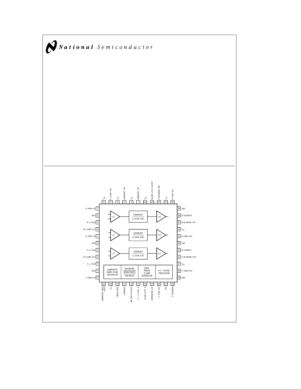
The LM1204 is a triple 150 MHz video amplifier system
designed specifically for high resolution RGB video display
applications. In addition to three matched video amplifiers,
the LM1204 contains a DC operated contrast control, a DC
operated drive control for each amplifier, and a dual clamping system for both brightness control and video blanking.
The LM1204 also contains a back porch clamp pulse generator which is activated by an externally supplied
g
H/HV
sync signal or by an external composite video signal. The
g
H/HV sync input will have priority over the composite vid-
eo input. A single
b
H/HV sync output is provided for the
automatically selected sync input signal. The back porch
clamp pulse width is user adjustable from 0.3 msto4ms.
The LM1204 video output stage will directly drive most
Hybrid or discrete CRT amplfier input stages without the
need for an external buffer transistor. The device has been
designed to operate from a 12V supply with all DC controls
operating over a 0V to 4V range providing for an easy interface to serial digital buss controlled monitors.
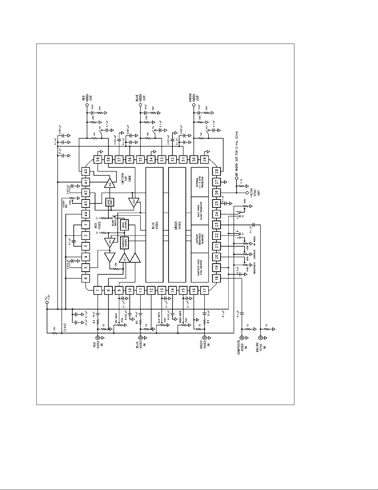
Block Diagram and Connection Diagram
Features
Y
Built-in video blanking function
Y
Built-in sync separator for composite video input
Y
Includes DC restoration of video signals
Y
Back porch clamp pulse width user adjustable
Y
DC control of brightness, contrast, blanking level, drive
and cutoff
Y
DC controls are 0V to 4V for easy interfacing to a
digitally controlled system
Key Specifications
Y
150 MHz large signal bandwidth (typ)
Y
2.3 ns rise/fall times (typ)
Y
0.1 dB contrast tracking (typ)
Y
g
3 dB drive (D gain) adjustments on R, G, B channels
(typ)
Applications
Y
High resolution CRT monitors
Y
Video AGC amplifier
Y
Wideband amplifier with gain and DC offset control
Top View
LM1204 150 MHz RGB Video Amplifier System
December 1994
Ordering Information
TL/H/11238– 1
Order Number LM1204V
See NS Package Number V44A
C
1995 National Semiconductor Corporation RRD-B30M115/Printed in U. S. A.
TL/H/11238
Page 2
Absolute Maximum Ratings (Note 1)
If Military/Aerospace specified devices are required,
please contact the National Semiconductor Sales
Office/Distributors for availability and specifications.
Supply Voltage, V
Pins 2, 4, 6, 19, 31, 41, 44 (Note 3) 13.5V
Peak Video Output Source Current
(Any One Amplifier) Pins 30, 35 or 39 30 mA
Voltage at Any Input Pin, V
MaximumgH Sync Input Voltage 5.5 V
Power Dissipation, PD (Above 25§C
Derate Based on iJAand TJ) 2.4W
CC
IN
GNDsV
s
V
IN
CC
Thermal Resistance, i
Junction Temperature, T
JA
J
52§C/W
150§C
ESD Susceptibility (Note 4) 2.5 kV
Storage Temperature
b
65§Cto150§C
Lead Temperature
Vapor Phase (60 seconds) 215
Infrared (15 seconds) 220
PP
Operating Ratings (Note 2)
C
§
C
§
Temperature Range 0§Cto70§C
Supply Voltage, V
CC
10.8VsV
CC
s
13.2V
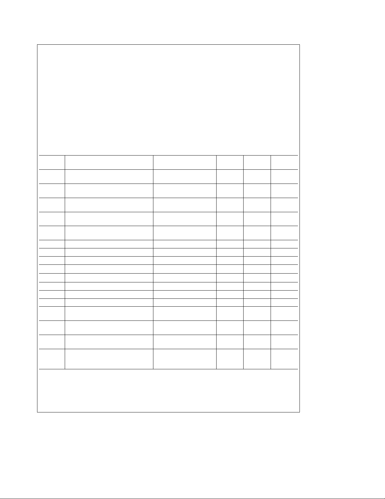
DC Electrical Characteristics (Video Amplifier Section)
The following specifications apply for VCC(pins 2, 4, 6, 19, 31, 36, 41 and 44)e12V and T
e
S1
B, S2eB, S3, 4, 5 closed, V9, 13, 15e2V, V20, 21, 22, 24, 43e0.5V unless otherwise specified; see test circuit,
Figure 1
.
Symbol Parameter Conditions
I
I
Blank
I
Blank
I
Clamp
I
Clamp
V
V
V
H
V
L
V
CM43
I
I
24h
I
24l
I
FB
I
BB
I
CB
24h
B
24l
Supply Current No Video or Sync Input
S
Signals, S1
e
A (Max)
Input Bias Current S1eA
(Pin 9, 13, 15, 20, 21 or 22) (Max)
Blank Gate Input High Current V24e4V
Blank Gate Input Low Current V24e0V
Feedback Input Current
(Pin 28, 33 or 38)
Blank Cap Charge Current V
a
Blank Cap Discharge Current V
b
32,37,42
32,37,42
e
0V 185 75 mA (Min)
e
5V
Blank Cap Bias Current (Pins 32, 37, 42) 20 nA
Clamp Cap Charge Current V
a
Blank Cap Discharge Current V
b
5,10,14
5,10,14
e
0V 185 75 mA (Min)
e
5V
Clamp Cap Bias Current (Pins 5, 10, 14) 20 nA
Blank Gate High Input Voltage Input Signal is Not Blanked 2 V (Min)
Blank Gate Low Input Voltage Input Signal is Blanked 0.8 V (Max)
Blank Comparator Offset Voltage Voltage between V43 and
Any One Video Output (Max)
Video Output High Voltage R
(Pins 30, 35, 40) V28, 33, 38
Video Output Low Voltage R
(Pins 30, 35, 40) V28, 33, 38
e
350X
L
L
e
350X
e
0V
e
4V
Common Mode Range of Blank 0.5 V(Min)
Comparator (Pins 43, 28, 33, 38)
e
25§C unless otherwise specified.
A
Typical Limit
(Note 5) (Note 6)
100 125
0.3 2
0.01 2
25
150 nA
b
185
b
185
b
75 mA (Min)
b
75 mA (Min)
250
8.7 7 V(Min)
0.1 0.5 V(Max)
4 V(Max)
Units
mA
mA
mA
(Max)
mA
(Max)
mV
2
Page 3
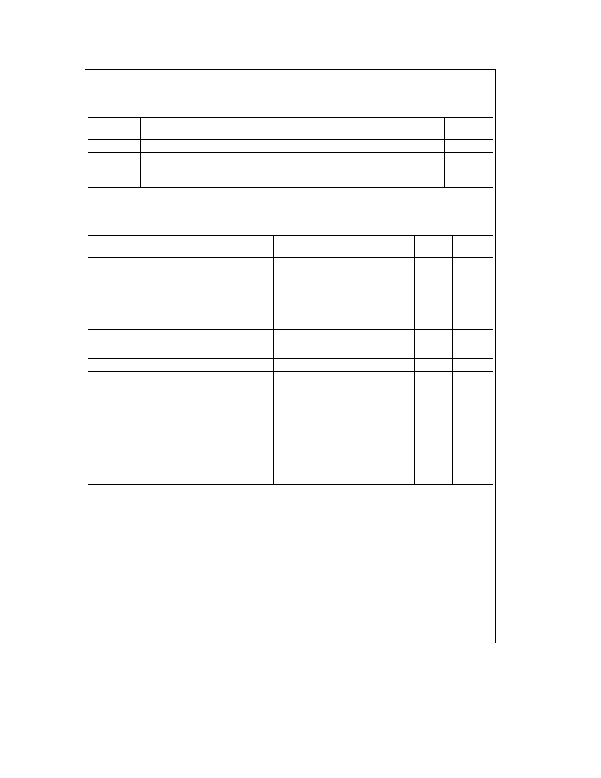
DC Electrical Characteristics (Sync Separator/Processor Section)
The following specifications apply for VCC(Pins 2, 4, 6, 19, 31, 36, 41 and 44)e12V and T
specified. S1
Circuit
Symbol Parameter Conditions
b
HV
b
HV
V
23
Figure 1
OH
OL
e
B, S2eB, S3, 4, 5 closed, V9, 13, 15e2V, V20, 21, 22, 24, 43e0.5V, unless otherwise specified; see Test
.
Typical Limit
(Note 5) (Note 6)
b
H Sync Output Logic High (Pin 26) 4.2 2.4 V(Min)
b
H Sync Output Logic Low (Pin 26) 0.1 0.4 V(Max)
Quiescent DC Voltage atgH
Sync Input
3V
e
25§C, unless otherwise
A
Units
AC Electrical Characteristics (Video Amplifier Section)
The following specifications apply for VCC(Pins 2, 4, 6, 19, 31, 36, 41 and 44)e12V and T
specified. S1
Figure 1
Symbol Parameter Conditions
R
IN
A
Vmax
DA
Vtrack
DA
V2V
DA
V0.5V
DGain D Gain Range (Pins 9, 13, 15) V9, 13, 15e0V to 4V
DV
O
f
b
3dB
THD Video Amplifier Distortion V
t
R
t
F
V
ISO (1 MHz)
V
ISO (130 MHz)
e
B, S2eB, S3, 4, 5 closed, V9, 13, 15, 21, 24, 43e4V, V20e2V, unless otherwise specified; see Test Circuit
.
Video Amplifier Input Resistance 20 kX
Maximum Video Amplifier Gain f
e
12 kHz 10 5.5 V/V(Min)
IN
Amplifier Gain (Contrast)
Tracking (Note 7)
Attenuation at 2V Ref: A
Attenuation at 0.5V Ref: A
V21e2V 6 dB
V
max
V21e0.5V 28 20 dB(Min)
V
max
Max Brightness Tracking Error (Note 8) 100 mV
Video Amplifier Bandwidth (Note 9) V
e
3.5 V
OUT
OUT
PP
e
1VPP,fe12 kHz 0.3 %
Video Output Rise Time (Note 9) Square Wave Input
V
OUT
e
3.5 VPP,R
e
350X
L
Video Output Fall Time (Note 9) Square Wave Input
V
OUT
e
3.5 VPP,R
e
350X
L
Video Amplifier 1 MHz
Isolation (Notes 9, 10)
Video Amplifier 130 MHz
Isolation (Notes 9, 10)
e
25§C, unless otherwise
A
Typical Limit
(Note 5) (Note 6)
Units
0.1 dB
g
3dB
150 MHz
2.0 ns
2.3 ns
b
50 dB
b
10 dB
3
Page 4
AC Electrical Characteristics (Sync Separator/Processor Section)
The following specifications apply for VCC(Pins 2, 4, 6, 19, 31, 36, 41 and 44)e12V and T
specified. S1
e
A, S2eB, S3, 4, 5 closed, V9, 13, 15, 20, 21, 43e2V, unless otherwise specified; see Test Circuit
e
25§C, unless otherwise
A
Figure 1
and Timing Diagram for input waveform.
Symbol Parameter Conditions
V
18(Min)
V
18(Max)
V
23
Composite Video Input Voltage S2eA, Inpute10% Duty
(Pin 18) Cycle, Test for Loss of BP (Min)
Composite Video Input Voltage Pulse at Pin 26
(Pin 18) (Max)
g
H Sync Input Voltage (Pin 23) Inpute10% Duty Cycle
Back Porch Clamp Pulse Width S2eA, Pin 26eBP Output
e
at V
1V (Max)
24
Back Porch Clamp Pulse Width
e
at V
4V (Max)
24
Typical Limit
(Note 5) (Note 6)
0.15
2
1.6
1 1.4
300 600
Units
V
V
V
(Min)
ms
ns
MaximumgH Sync Input Frequency 600 KHz
D
HI
D
LO
t
pdl1
t
pdh1
t
pd1
t
pdl2
t
pdh2
t
pd2
t
pdl2–tpdl1
Note 1: Absolute Maximum Ratings indicate limits beyond which damage to the device may occur.
Note 2: Operating Ratings indicate conditions for which the device is functional, but do not guarantee specific performance limits. For guaranteed specifications
and test conditions, see the Electrical Characteristics. The guaranteed specifications apply only for the test conditions listed. Some performance characteristics
may degrade when the device is not operated under the listed test conditions.
Note 3: V
Note 4: Human body model, 100 pF discharged through a 1.5 kX resistor.
Note 5: Typical specifications are specified at
Note 6: Tested limits are guaranteed to National’s AOQL (Average Outgoing Quality Level).
Note 7: DA
gain change between any two amplifiers with the contrast voltage, V21, at either 4V or 2V measured relative to an A
max, the three amplifier gains might be 17.4 dB, 16.9 dB and 16.4 dB and change to 7.3 dB, 6.9 dB and 6.5 dB respectively for V21e2V. This yields the measured
typical
Note 8: Brightness tracking error is measured with all three video channels set for equal gain. The measured value is limited by the resolution of the measurement
equipment.
Note 9: When measuring video amplifier bandwidth or pulse rise and fall times, a double sided full ground plane printed circuit board is recommended. Video
amplifier isolation tests also require this printed circuit board. The measured rise and fall times are effective rise and fall times, taking into account the rise and fall
times of the generator.
Note 10: Measure output levels of either undriven amplifier relative to the driven amplifier to determine channel isolation. Terminate the undriven amplifier inputs.
Max Duty Cycle of Active High Test for Loss of Sync
H Sync (Pin 23) at Pin 26
Max Duty Cycle of Active Low
H Sync (Pin 23)
g
H Sync Input tobH Sync Inpute10% Duty Cycle
Output Low Delay
g
H Sync Input tobH Sync Inpute10% Duty Cycle
Output High Delay
g
H Sync Input Trailing Edge to Inpute10% Duty Cycle,
Back Porch Clamp Output Delay S2
e
A
Composite Video Input tobH Inpute10% Duty Cycle
Sync Output Low Delay
Composite Video Input tobH Inpute10% Duty Cycle
Sync Output High Delay
Composite Video Input Trailing Inpute10% Duty Cycle
Edge to Back Porch Clamp Output Delay S2
e
A
Composite Video andgH Sync Input Inpute10% Duty Cycle
b
to
H Sync Output Delta Delay
supply pins 2, 4, 6, 19, 31, 36, 41 and 44 must be externally wired together to prevent internal damage during VCCpower on/off cycle.
CC
a
25§C and represent the most likely parametric norm.
tracking is a measure of the ability of any two amplifiers to track each other and quantifies the matching of the three attenuators. It is the difference in
V
g
0.1 dB channel tracking.
22 %
22 %
100 ns
65 ns
70 ns
106 ns
68 ns
78 ns
6ns
max condition V21e4V. For example, at A
V
PP
PP
PP
V
4
Page 5
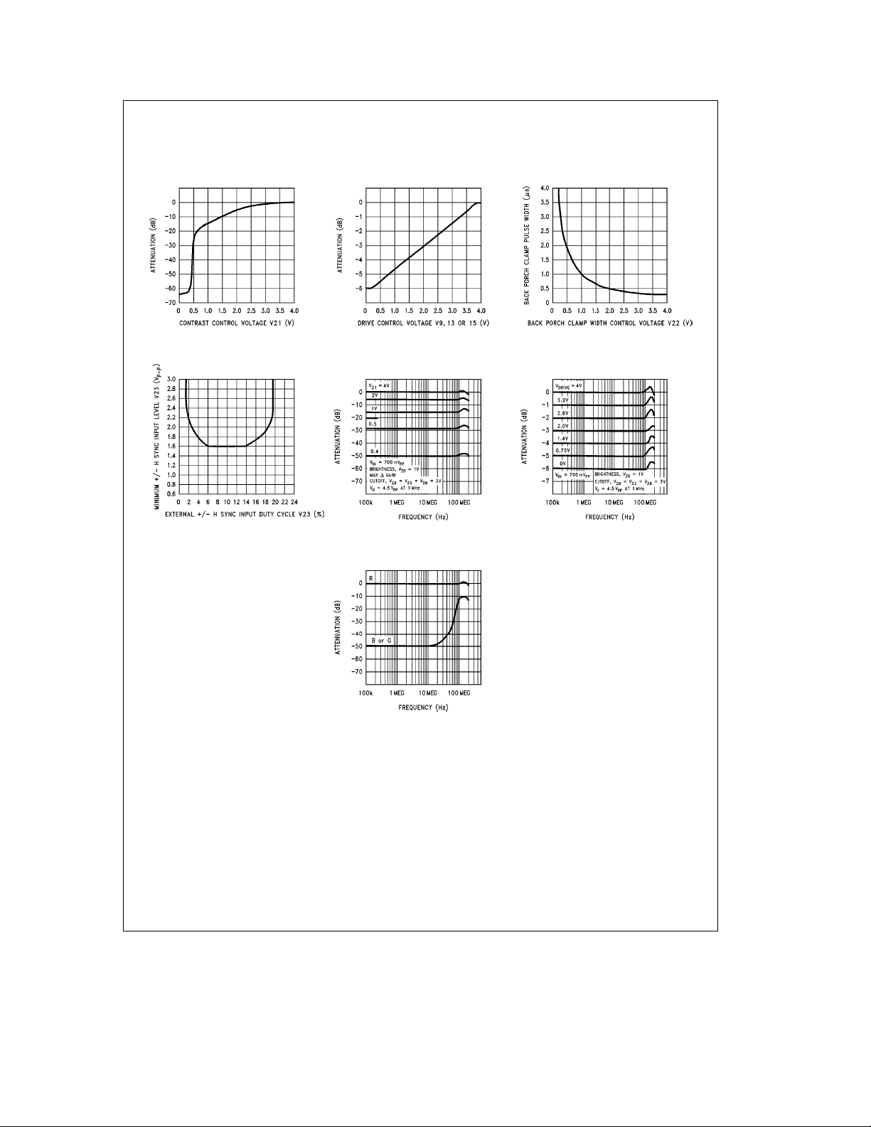
Typical Performance Characteristics V
CC
e
12V, T
e
25§C unless otherwise specified
A
Attenuation vs Contrast
Control Voltage (
Minimum External
Sync Input Level (V
vs Input Duty Cycle (%)
f
e
g
H
PP
12 kHz)
Attenuation vs Drive
Control Voltage (
f
e
12 kHz)
Back Porch Clamp Pulse
Width vs Pin 22 Voltage
)
Contrast vs Frequency Drive Control vs Frequency
Crosstalk vs Frequency
TL/H/11238– 2
5
Page 6
TL/H/11238– 3
FIGURE 1. LM1204 Test Circuit
6
Page 7

Timing Diagram
Input/Output Stages
b
H Sync Output Stage
TL/H/11238– 4
Composite Video Input
TL/H/11238– 6
TL/H/11238– 5
Video Output Stage
TL/H/11238– 21
7
Page 8

Input/Output Stages (Continued)
g
H/HV Sync Input
TL/H/11238– 7
Video Input Stage
TL/H/11238– 8
Pin Descriptions
VCC(Pins 2, 4, 6, 19, All VCCpins must be externally wired together. For stable operation, each supply pin should be
31, 36, 41, 44) bypassed with a 0.01 mF and a 0.1 mF capacitor connected as close to the pin as is possible.
Contrast Cap (Pins 1, 3) An external decoupling capacitor of value 0.1 mF should be connected between pins 1 and 3 for
R Clamp Cap (Pin 5) A 0.022 mFto0.1mF capacitor should be connected from this pin to ground. This capacitor allows
B Clamp Cap (Pin 10) A 0.022 mFto0.1mF capacitor should be connected from this pin to ground. This capacitor allows
G Clamp Cap (Pin 14) A 0.022 mFto0.1mF capacitor should be connected from this pin to ground. This capacitor allows
R Video In (Pin 7) This is the input for the red channel video signal, the signal should be AC coupled to the input through
B Video In (Pin 11) This is the input for the blue channel video signal, the signal should be AC coupled to the input
G Video In (Pin 17) This is the input for the green channel video signal, the signal should be AC coupled to the input
R D Gain (Pin 9) This is the gain adjustment pin for the red video channel. A 0V to 4V
B D Gain (Pin 13) This is the gain adjustment pin for the blue video channel. A 0V to 4 V
G D Gain (Pin 15) This is the gain adjustment pin for the green video channel. A 0V to 4 V
Compose Video Input This is the sync separator input pin. For Sync on Green systems, the green channel video signal
(Pin 18) should be AC coupled to pin 18 through a 0.1 mF capacitor.
Brightness Control If the LM1204 is used without blanking then this pin should be biased at 2.0 V
(Pin 20) for all three video channels is now controlled by pin 43 (blank level adjust pin). See
Contrast Control This pin simultaneously controls the gain of all three video channels. A 0V to 4 VDCinput voltage is
(Pin 21) applied to this pin, with 0V corresponding to minimum gain (i.e., maximum attenuation of video signal)
contrast control.
clamping of the red channel video signal to the reference black level.
clamping of the blue channel video signal to the reference black level.
clamping of the green channel video signal to the reference black level.
a10mF capacitor.
through a 10 mF capacitor.
through a 10 mF capacitor.
voltage is applied to this pin to
vary the gain of the red channel. Usually, the red channel is set for maximum gain and the gains of the
DC
blue and green channels are reduced relative to the red channel until white balance is achieved on
the CRT screen.
voltage is applied to this pin
to vary the gain of the blue channel.
to vary the gain of the green channel.
DC
voltage is applied to this pin
DC
. Brightness control
DC
Figure 4
.Ifthe
LM1204 is used with blanking then this pin allows the user to simultaneously DC offset the video
portion of the output signals of all three channels thus allowing brightness control (See
Figure 5
).
and 4V corresponding to maximum gain (i.e., minimum attenuation of the video signal).
8
Page 9

Pin Descriptions (Continued)
Back Porch Clamp Width The LM1204 provides DC restoration or clamping during the back porch interval of the video signal.
Adjust (Pin 22) The width of LM1204’s internally generated back porch clamp signal can be varied by applying a 0V
g
H Sync In (Pin 23) This is the external sync input pin, it accepts a negative or positive polarity signal, either horizontal
Blank Gate In (Pin 24) This is the blank gate input pin. The LM1204 allows video blanking at the preamplifier. If blanking is
Integrator Cap (Pin 25) A 0.1 mF capacitor should be connected from this pin to ground. This capacitor allows the LM1204 to
b
H Sync Out (Pin 26) This output pin provides a negative polarity horizontal sync signal for other system uses. There is
G Feedback (Pin 28) This is the cutoff adjustment input for the green video channel. The green video output signal from
B Feedback (Pin 33) This is the cutoff adjustment input for the blue video channel. The blue video output signal from pin
R Feedback (Pin 38) This is the cutoff adjustment input for the red video channel. The red video output signal from pin 40
G Video Output This is the green channel video output.
(Pin 30)
B Video Output This is the blue channel video output.
(Pin 35)
R Video Output This is the red channel video output.
(Pin 40)
G Blank Clamp Cap A 0.022 mFto0.1mF capacitor should be connected from this pin to ground. This capacitor allows
(Pin 32) blanking for the green video channel.
B Blank Clamp Cap A 0.022 mFto0.1mF capacitor should be connected from this pin to ground. This capacitor allows
(Pin 37) blanking for the blue video channel.
R Blank Clamp Cap A 0.022 mFto0.1mF capacitor should be connected from this pin to ground. This capacitor allows
(Pin 42) blanking for the red video channel.
Blank Level Adjust This pin serves two functions depending on whether the LM1204 is used with blanking or without
(Pin 43) blanking. If blanking is not selected then pin 20 should be biased at 2.0 V
GND (Pins 8, 12 16, 27, Ground. All ground pins must be connected to the ground plane.
29, 34, 39)
to4V
voltage to this pin. The back porch clamp signal width can be varied from approximately
DC
0.3 msto4.0ms by applying 4V to 0.5V respectively. By connecting the blank gate input pin (pin 24)
to V
, the back porch clamp pulse can be monitored on thebH Sync output pin (pin 26). See
CC
Figures 4
and5. By connecting pin 22 to VCC, the LM1204 functions as a non-gated amplifier
requiring no clamping. See Section 4 under application hints for further information.
sync or a composite sync (1.2 V
polarity (TTL compatible) horizontal sync or composite sync output on pin 26. If the composite video
minimum amplitude). The LM1204 also provides a negative
PP
input (pin 18) is not used then an H Sync signal should be AC coupled to this pin through a 0.1 mF
capacitor. The
g
H Sync input has priority over the composite video input if both signals are present.
desired then a TTL compatible, negative polarity blanking signal should be applied to this pin. During
the blanking interval, all three video outputs are level shifted to the blank level set by the voltage at
pin 43. If blanking is not required then, pin 24 should be biased at 4V.
Connecting pin 24 to V
signal. The user can observe the change in back porch width as the potential at pin 22 is varied (see
Figures 4
integrate the
and5).
g
H Sync input signal and genreate the proper polarity switch forbH Sync output.
approximately 100 ns delay between the
will cause pin 26 to output the internally generated back porch clamp
CC
g
H Sync input signal at pin 23 and thebH Sync output
signal at pin 26.
Connecting pin 24 to V
signal. The user can observe the change in back porch clamp pulse width as the potential at pin 22 is
varied (See
Figures 4
will cause pin 26 to output the internally generated back porch clamp
CC
and5).
pin 30 is fed back to this input through a potentiometer thus allowing the user to individually adjust
the cutoff (black reference) level for each gun. The signal level at this pin should be between 0.5V
and 4V.
35 is fed back to this input through a potentiometer thus allowing the user to individually adjust the
cutoff (black reference) level for each gun. The signal level at this pin should be between 0.5V and
4V.
is fed back to this input through a potentiometer thus allowing the user to individualy adjust the cutoff
(black reference) level for each gun. The signal level at this pin should be between 0.5V and 4V.
and pin 43 assumes the
role of brightness control. Varying the potential at pin 43 will simultaneously DC offset the video
output signals of all three channels (See
Figure 4
). If the LM1204 is used with blanking then during
DC
the blanking interval, all three video output signals will be level shifted to the blank level. The desired
blank level can be set by adjusting the potential at pin 43. Brightness control is now made possible
by varying the potential at pin 20. Adjusting the brightness control DC offsets the video portion of the
signal relative to the fixed blank level (all channels are affected simultaneously). See
Figure 5
.
9
Page 10

Applications Hints
The LM1204 is a wideband video amplifier system designed
specifically for high resolution RGB CRT monitors. The device includes circuitry for DC restoration of video signals
and also allows contrast and brightness control. DC restoration is done during the back porch interval of the video signal. An internal sync separator generates a back porch
clamp signal either from a ‘‘Sync on Green’’ signal applied
to the composite video input (pin 18) or from an externally
g
supplied
g
is not present then the device syncs off the composite video
input. The internally generated back porch clamp pulse
width is user adjustable.
A blanking function is also included. This allows the user to
cutoff the beam current in the CRT’s guns during the blanking interval thereby preventing horizontal retrace lines from
being visible. Normally blanking is done by applying a high
voltage pulse at the grid. However, blanking at the cathode
using the LM1204 leads to ease of design and lowered cost.
Figure 2
nel and the control logic. The two modes of operation, with
and without blanking, are described below in detail.
H Sync signal . The LM1204 first looks at the
H Sync input (pin 23), if an external horizontal sync signal
shows the block diagram of the green video chan-
1.0 Operation without Blanking
For operation without blanking, the blank gate input (pin 24)
should be connected to
parator to connect switch S2 to position Y (See
Furthermore, the brightness control input pin (pin 20) should
be biased at a potential between 1V (Min) and 3.8V (Max), it
is best to bias this pin at 2V. The video signal is AC coupled
to the input of the LM1204 as shown for the green channel
in
Figure 2
nal (See
clamping pulse goes low, causing switches S1A and S1B to
be closed. The closure of S1A causes g
itor C2 to a potential determined by the DC voltage at pin
20. This allows g
coupled video signal at the input of A1. When the back
porch clamping pulse is high, S1A and S1B are opened.
With S1A open, g
now holds the DC bias voltage. The transconductance
stage g
and holds the input of A1 at the desired DC bias.
The LM1204 uses black level clamping at the back porch of
the video signal to accomplish DC restoration. The transconductance stage g
clamp period to provide a sample and hold function. During
the back porch clamp period, DC feedback from LM1204’s
video output is compared with the voltage set by potentiometer R9. Depending on A2’s output voltage, C6 is either
charged or discharged so that the feedback loop consisting
of g
black level. All this occurs during the back porch clamp period. During the video portion of the signal, g
and C6 holds the fixed black level reference voltage. The
beginning of each new line on the raster always starts from
a fixed reference black level thus restoring the DC component of each line.
A2 is a summing amplifier that adds a DC offset component
from g
R9 will DC offset the output signals of all three channels
thus providing brightness control. Individual cutoff adjust-
. During the back porch interval of the video sig-
Figure 3
1 therefore functions as a sample and hold device
m
2 and A2 is stabilized and the output is clamped to the
m
2 to the video signal from the multiplier. Adjusting
m
a
4V. This causes the blank com-
Figure 2
), the internally generated back porch
1 to charge capac-
m
1 to set up an average DC bias for the AC
m
1 is effectively disconnected from C2, C2
m
2 is enabled during the back porch
m
2 is disabled
m
ment for each channel is done by varying the feedback voltage at each of the R, G and B feedback inputs (Pins 38, 28
and 33). For example, cutoff adjustment for the green channel is done by potentiometer R8 shown in
Adjusting the contrast control (potentiometer R3 in
2
) varies the peak to peak amplitude (includes sync tip if
present) of all three video output signals relative to their
black reference level. The D Gain adjust (pins 9, 15 and 13
for R, G, and B channels respectively) allows the user to
individually adjust the AC gain of each channel. For example
the AC gain of the green channel is adjusted using potentiometer R5 as shown in
is set for maximum gain and the gains of the blue and green
channels are reduced until white balance is achieved on the
CRT monitor’s screen.
operation without blanking.
Figure 2
Figure 4
. Normally the red channel
shows the adjustments for
2.0 Operation with Blanking
Much of what was discussed in Section 1.0 also applies
when the LM1204 is used with the blanking function. However, there are notable differences as described herein. For
operation with blanking, a TTL compatible blanking signal
must be applied to the blank gate input (pin 24).
During the blanking period, the blanking comparator connects switch S2 to position X (See
the LM1204 to level shift the video output signal to the blank
level. Adjusting R9 will adjust the blank level of all three
channels. Individual blank level adjustment for each chan-
).
nel is done by varying the feedback voltage at each of the
R, G and B feedback inputs (pin 38, 28 and 33). In
this is done by adjusting potentiometer R8 for the green
channel.
During the video portion of the video signal, S2 is connected
to position Y. Brightness control is now accomplished by
varying the potential at the brightness control pin (pin 20).
Adjusting R6 offsets the video portion of all three output
signals relative to the fixed blank level, restoring the DC
level of the video signal.
operation with blanking.
Figure 5
Figure 2
shows the adjustments for
3.0 Stability Considerations
For optimum performance and stable operation, a double
sided PC board with adequate ground plane is essential.
Moreover, soldering the LM1204 on to the PC board will
yield best results. Each supply pin (pins 2, 4, 6, 19, 31, 36,
41 and 44) should be bypassed with a 0.01 mF and a 0.1 mF
capacitor connected as close to the supply pin as is possible.
When driving the LM1204 from a 75X video source, the
cable is terminated with 75X to minimize reflections caused
by transmission line effects. However, the input impedance
of LM1204 is capacitive and is also affected by the stray
capacitance of the PC board. Thus the input impedance is a
function of frequency. This changes the impedance of the
cable termination. This can introduce overshoot and ringing
in LM1204’s pulse response. A 100X resistor in series with
the blocking capacitor at the video input will minimize overshoot and ringing (see
empirically determined. 100X is a good starting value.
Since the LM1204 is a wide bandwidth amplifier with high
gain at high frequencies, the device may oscillate when driving a large capacitive/inductive load. To prevent oscillation,
the amplifier’s gain is rolled off at high frequencies. This is
accomplished by an RC network comprised of a resistor in
Figure 8
). The value of the resistor is
Figure 2
.
). This causes
Figure 2
Figure
10
Page 11

3.0 Stability Considerations (Continued)
series with a capacitor connected from the video output pin
to ground (see Test Circuit,
resistor in series with 10 pF is quite adequate for most applications. However, if oscillations don’t cease then the value
of the resistor should be decreased or the value of the capacitor should be increased or a combination of the two.
Figure 1
). A 110X to 200X
LM1204
Non-Gated High
Frequency Application
By connecting the back porch width adjust pin (pin 22) to
V
, the LM1204 functions as a non-gated amplifier requir-
CC
ing no sync or blanking signals.
frequency amplifier with variable gain and DC offset control.
In this mode of operation, filtered DC feedback must be
provided to pins 28, 33 and 38 as shown in
Figure 9
shows a triple high
Figure 9
.
FIGURE 2. Block Diagram Showing Timing Circuitry and Green Video Channel
FIGURE 3. Composite Video and Timing Signals
11
TL/H/11238– 9
TL/H/11238– 10
Page 12

TL/H/11238– 11
TL/H/11238– 12
FIGURE 4. LM1204 Adjustments without Blanking
12
TL/H/11238– 13
TL/H/11238– 14
Page 13

FIGURE 5. LM1204 Adjustments with Blanking
13
TL/H/11238– 15
Page 14

Typical Applications Circuits
Figure 4
TL/H/11238– 16
pin should be bypassed with a 0.01 mF and a 0.1 mF capacitor connected as close to the pin as is possible.
CC
for explanation of adjustments). Each V
FIGURE 6. The LM1204 driving cascode CRT video amplifiers and operating without blanking. Brightness control is accomplished by potentiometer R12 (See
14
Page 15

Typical Applications Circuits (Continued)
TL/H/11238– 17
Figure 5
pin should be bypassed with a 0.01 mF and a 0.1 mF capacitor connected as close to the pin as is possible.
CC
for explanation of adjustments. Each V
FIGURE 7. The LM1204 driving cascode CRT video amplifiers and operating with blanking. The video signal is level shifted to the user adjustable blank level
during the blanking period. Brightness control DC offsets the video signal relative to the fixed blank level and is accomplished by potentiometer R7. See
15
Page 16

Typical Applications Circuits (Continued)
FIGURE 8. Complete circuitry for an RGB CRT video board using the LM1204 and LH2426AS.
The video output signals from LH2426AS are AC coupled and diode clamped to greater than 80V.
16
TL/H/11238– 18
Page 17

Typical Applications Circuits (Continued)
FIGURE 8. (Continued)
17
TL/H/11238– 20
Page 18

Typical Applications Circuits (Continued)
TL/H/11238– 19
pin should be
CC
bypassed with a 0.01 mF and a 0.1 mF capacitor connected as close to the pin as is possible.
FIGURE 9. Three channel high frequency amplifier with gain and DC offset control (non-video application). Each V
18
Page 19

19
Page 20

Physical Dimensions inches (millimeters)
LM1204 150 MHz RGB Video Amplifier System
Order Number LM1204V
NS Package Number V44A
LIFE SUPPORT POLICY
NATIONAL’S PRODUCTS ARE NOT AUTHORIZED FOR USE AS CRITICAL COMPONENTS IN LIFE SUPPORT
DEVICES OR SYSTEMS WITHOUT THE EXPRESS WRITTEN APPROVAL OF THE PRESIDENT OF NATIONAL
SEMICONDUCTOR CORPORATION. As used herein:
1. Life support devices or systems are devices or 2. A critical component is any component of a life
systems which, (a) are intended for surgical implant support device or system whose failure to perform can
into the body, or (b) support or sustain life, and whose be reasonably expected to cause the failure of the life
failure to perform, when properly used in accordance support device or system, or to affect its safety or
with instructions for use provided in the labeling, can effectiveness.
be reasonably expected to result in a significant injury
to the user.
National Semiconductor National Semiconductor National Semiconductor National Semiconductor
Corporation Europe Hong Kong Ltd. Japan Ltd.
1111 West Bardin Road Fax: (
Arlington, TX 76017 Email: cnjwge@tevm2.nsc.com Ocean Centre, 5 Canton Rd. Fax: 81-043-299-2408
Tel: 1(800) 272-9959 Deutsch Tel: (
Fax: 1(800) 737-7018 English Tel: (
National does not assume any responsibility for use of any circuitry described, no circuit patent licenses are implied and National reserves the right at any time without notice to change said circuitry and specifications.
Fran3ais Tel: (
Italiano Tel: (
a
49) 0-180-530 85 86 13th Floor, Straight Block, Tel: 81-043-299-2309
a
49) 0-180-530 85 85 Tsimshatsui, Kowloon
a
49) 0-180-532 78 32 Hong Kong
a
49) 0-180-532 93 58 Tel: (852) 2737-1600
a
49) 0-180-534 16 80 Fax: (852) 2736-9960
 Loading...