

Page 1
LM1201 Video Amplifier System
General Description
The LM1201 is a wideband video amplifier system intended
for high resolution monochrome or RGB monitor applications. In addition to the wideband video amplifier the
LM1201 contains a gated differential input black level clamp
comparator for brightness control and an attenuator circuit
for contrast control. The LM1201 also contains a voltage
reference for the video input. For medium resolution RGB
color monitor applications also see the LM1203 Video Amplifier System data sheet.
Features
Y
Wideband video amplifier (200 MHz
Y
Attenuator circuit for contrast control (l40 dB range)
Y
Externally gated comparator for brightness control
@
b
3 dB)
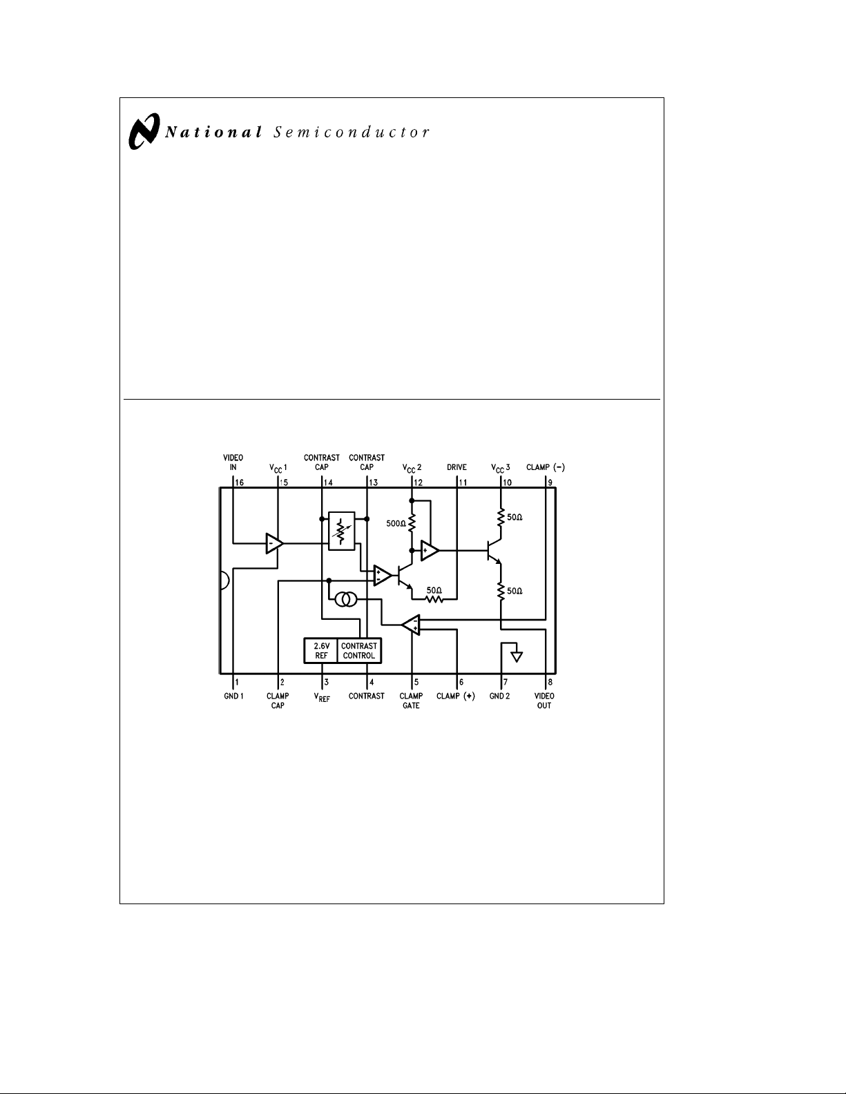
Block and Connection Diagram
Y
Y
Y
Typical Applications
Y
Y
Y
Y
Y
Y
Y
Y
LM1201 Video Amplifier System
January 1995
Provisions for external gain set and peaking of video
amplifier
Video input voltage reference
Low impedance output driver
CRT video amplifiers
Video switches
High frequency video preamplifiers
Wideband gain controls
PC monitors
Workstations
Facsimile machines
Printers
FIGURE 1
Order Number LM1201M or LM1201N
See NS Package Number M16A or N16E
C
1996 National Semiconductor Corporation RRD-B30M56/Printed in U. S. A.
TL/H/10006
TL/H/10006– 1
Page 2
Absolute Maximum Ratings
If Military/Aerospace specified devices are required,
please contact the National Semiconductor Sales
Office/Distributors for availability and specifications.
Supply Voltage V
to Ground Pins, 1, 7 13.5V
Voltage at Any Input Pin (V
Pins 10, 12, 15
CC
IN
)V
CC
t
V
IN
t
GND
Video Output Current (I8)28mA
e
Package Power Dissipation at T
(Above 25
C derate based on (iJAand TJ)
§
Package Thermal Resistance (i
25§C 1.56W
A
) N16E 80§C/W
JA
Package Thermal Resistance (iJA) M16A 100§C/W
Junction Temperature (TJ) 150§C
Storage Temperature Range (T
Lead Temperature (Soldering, 10 sec.) 265§C
ESD Susceptibility 2 kV
Human body model: 100 pF discharged through a 1.5 kX
resistor
Operating Ratings (Note 4)
Temperature Range 0§Ctoa70§C
Supply Voltage (V
CC
b
)
STG
65§Ctoa150§C
) 10.8VsV
CC
s
13.2V
Electrical Characteristics See Test Circuit (Figure 2), T
DC Static Tests S9 Open; V4
e
6V; V5e0V; V6e2.0V unless otherwise stated
A
e
25§C; V
Symbol Parameter Conditions Typical Limit Limit
I
S
V
3
Supply Current VCCPins 12, 15 Only 45 57 mA(max)
Video Input Reference Voltage 2.65 2.4 V(min)
e
V
CC1
CC2
Tested Design
(Note 1) (Note 2)
e
e
V
12V
CC3
Units
(Limits)
2.95 V(max)
I
16
V
5L
V
5H
I
5L
I
5H
I
a
2
I
b
2
V
8L
V
8H
V
OS
AC Dynamic Tests S9 Closed, V
Symbol Parameter Conditions Typ
Av max Video Amplifier Gain V
DAv 5V Attenuation@5V Ref: Av max, V
DAv 2V Attenuation@2V Ref: Av max, V
THD Video Amplifier Distortion V
f(b3dB) Video Amplifier Bandwidth (Note 3) V
t
r
t
f
Note 1: These parameters are guaranteed and 100% production tested.
Note 2: Design limits are guaranteed (but not 100% production tested). These limits are not used to calculate outgoing quality levels.
Note 3: When measuring video amplifier bandwidth or pulse rise and fall times, a double sided full ground plane printed circuit board without socket is recommend-
ed.
Note 4: Operating Ratings indicate conditions of which the device is functional, but does not guarantee specific performance limits. For guaranteed specifications
and test conditions, see Electrical Characteristics. The guaranteed specifications apply only for the test conditions listed. Some performance characteristics may
degrade when the device is not operated under the listed test conditions.
Video Input Bias Current (V3–V16)/10 kX 5.0 20 mA(max)
Clamp Gate Low Input Voltage Clamp Comparator On 1.2 0.8 V(min)
Clamp Gate High Input Voltage Clamp Comparator Off 1.6 2.0 V(max)
Clamp Gate Low Input Current V
Clamp Gate High Input Current V
Clamp Cap Charge Current V
Clamp Cap Discharge Current V
Video Output Low Voltage V
Video Output High Voltage V
5
5
2
2
2
2
Comparator Input Offset Voltage V6–V
e
0V, V
5
e
0V
e
12V 0.005 1 mA(max)
e
0V 1 0.55 mA(min)
e
5V
e
0V 0.5 0.9 V(max)
e
5V 8.5 8.0 V(min)
9
e
4V
6
b
0.5
b
1
g
0.5
b
5.0 mA(max)
b
0.55 mA(min)
g
25 mV(max)
Tested Design Units
Limit (Note 1) Limit (Note 2) (Limits)
e
12V 8 5.5 V/V(min)
4
Output Rise Time (Note 3) V
Output Fall Time (Note 3) V
e
5V
4
e
2V
4
e
4
e
4
e
O
e
O
5V, V
12V, V
4V
p-p
4V
p-p
e
1V
O
p-p
e
100 mV
O
b
10 dB
b
45 dB
0.3 %
200 170 MHz(min)
rms
2.5 ns
3ns
http://www.national.com 2
Page 3
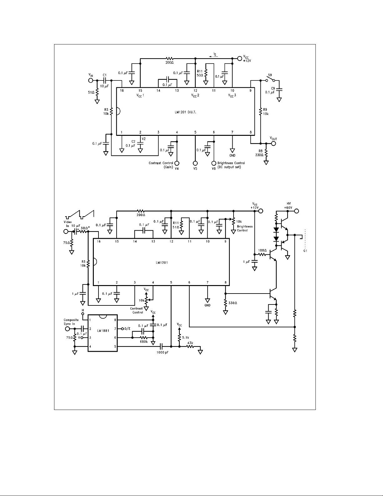
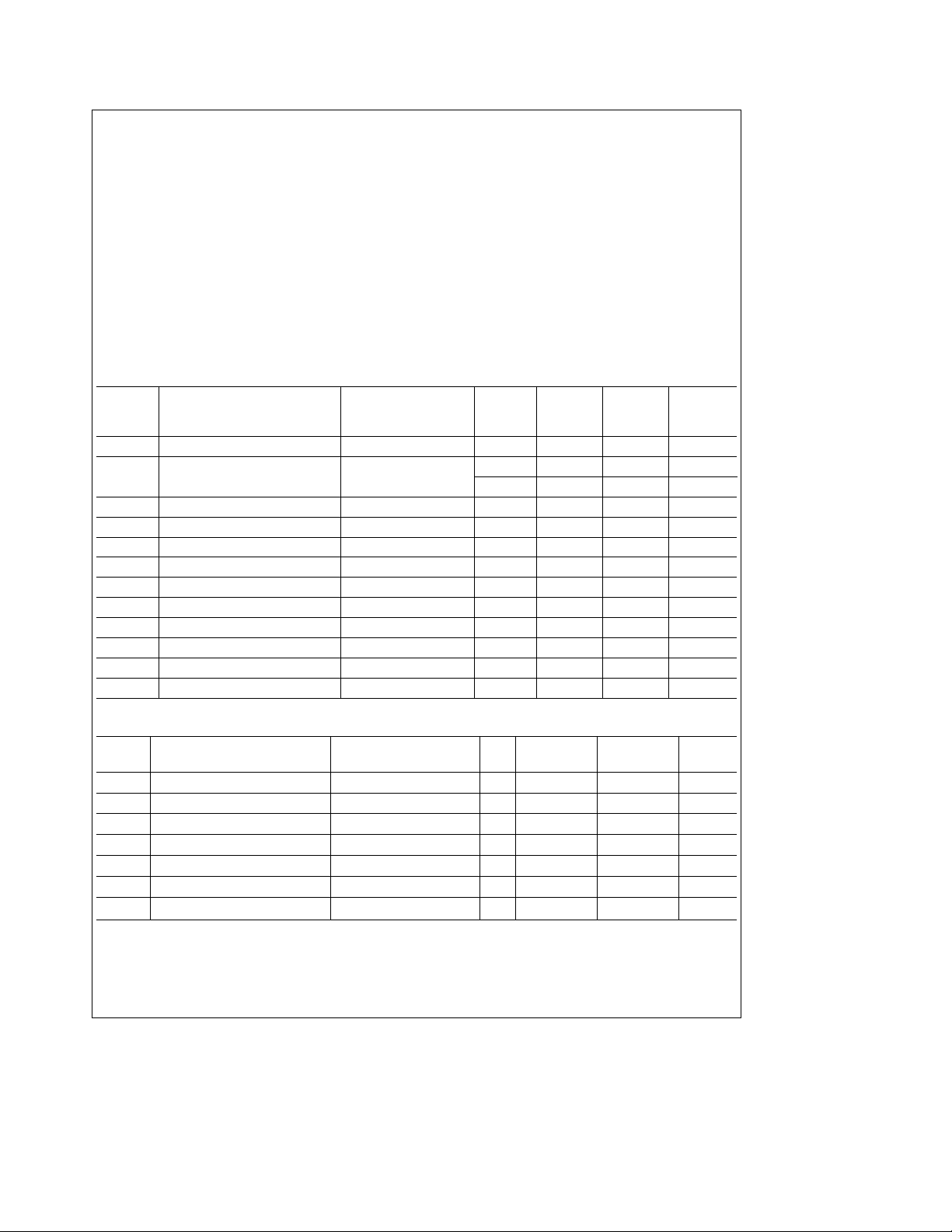
FIGURE 2. LM1201 AC/DC Test Circuit
TL/H/10006– 2
Note: When V
duty cycle square waves can be used for test purposes. The low frequency dominant pole is determined by C2 at Pin 2. Capacitor C9 at pin 9 prevents overloading
the clamp comparator inverting input. See applications section for additional information.
s
0.8V and S9 is closed, DC feedback around the Video Amplifier is provided by the clamp comparator. Under these conditions sine wave or 50%
5
FIGURE 3. Typical Application of the LM1201
TL/H/10006– 3
* 30X resistor is added to the input pin for protection against current surges coming from the 10 mF input capacitor. By increasing this resistor to well over 100X
the rise and fall times of the LM1201 can be increased for EMI considerations.
http://www.national.com3
Page 4
APPLICATIONS INFORMATION
Figure 4
shows the block diagram of a typical analog monochrome monitor. The monitor is used with CAD/CAM work
stations, PCs, arcade games and in a wide range of other
applications that benefit from the use of high resolution display terminals. Monitor characteristics may differ in such
ways as sweep rates, screen size, or in video amplifier
speed but will still be generally configured as shown in
ure 4
. Separate horizontal and vertical sync signals may be
Fig-
required or they may be contained as a composite signal in
the video input signal. The video input signal is usually
supplied by coaxial cable which is terminated in 75X at the
monitor input and internally AC coupled to the video amplifier. The input signal is approximately 1V peak-to-peak in amplitude and at the input of the high voltage video section,
approximately 6V peak-to-peak. At the cathode of the CRT
the video signals can be as high as 60V peak to peak. The
block in
Figure 4
labeled ‘‘Video Amplification with DC Controlled Gain/Black Level’’ contains the function of the
LM1201 video amplifier system.
FIGURE 4. Typical Monochrome Monitor Block Diagram
TL/H/10006– 4
http://www.national.com 4
Page 5
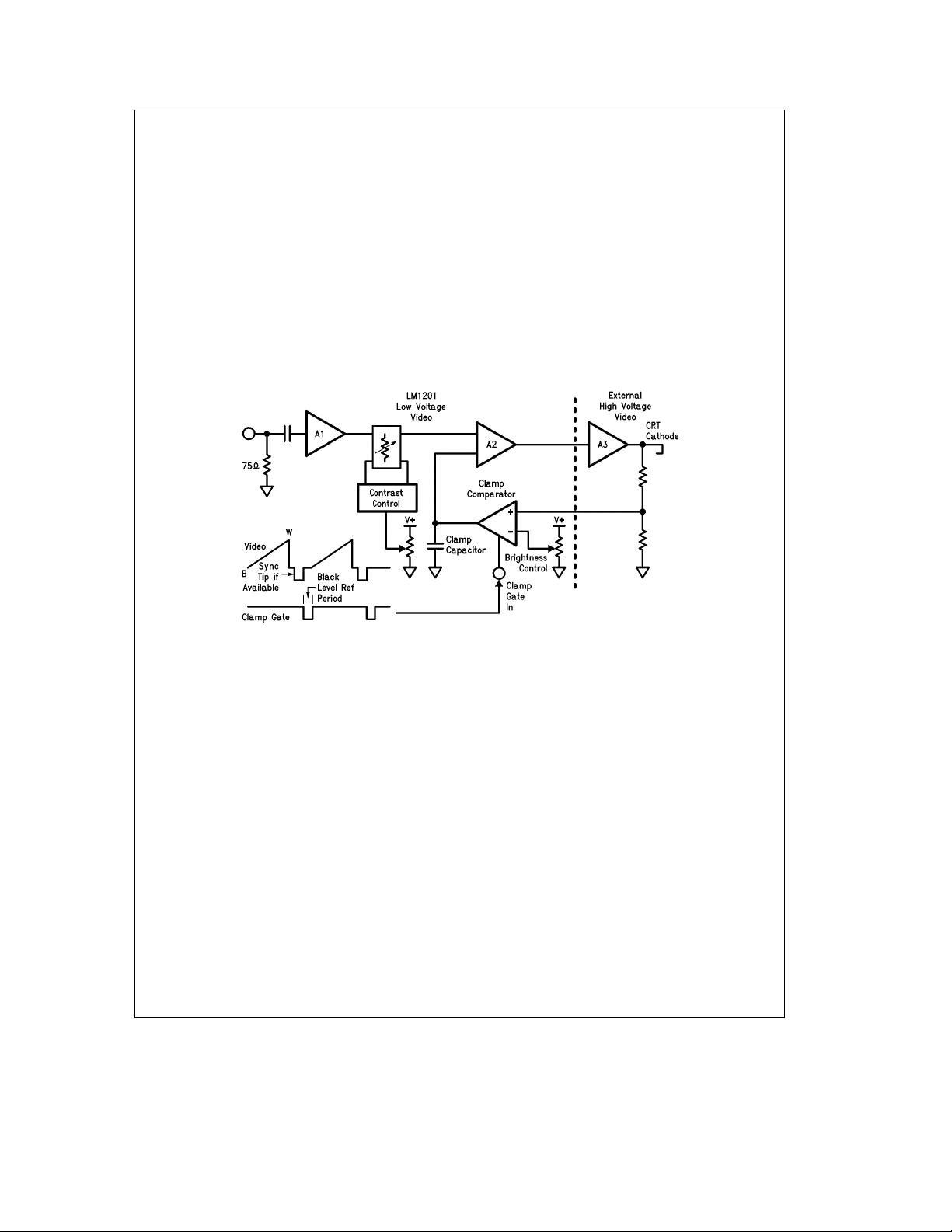
Circuit Description
Figure 5
is a block diagram of the LM1201 along with the
contrast and brightness controls. The contrast control is a
DC operated attenuator which varies the AC gain of the
amplifier without introducing any signal distortions or DC
output shift. The brightness control function requires a
‘‘sample and hold’’ circuit (black level clamp) which holds
the DC bias of the video amplifier and CRT cathodes constant during the black level reference portion of the video
waveform. The clamp comparator, when gated on during
this reference period, will charge or discharge the clamp
capacitor until the non-inverting input of the clamp comparator matches that of the inverting input voltage which was set
by the brightness control.
Figure 6
is a simplified schematic of the LM1201 video amplifier along with the recommended external components.
The IC pin numbers are circled with all external components
shown outside of the dashed line. The video input is applied
to pin 16 via the 10 mF coupling capacitor. DC bias to the
video input is through the 10 kX resistor which is connected
to the 2.6V reference at pin 3. The low frequency roll-off of
the amplifier is set by these two components. Transistor Q1
buffers the video signal to the base of Q2. The Q2 collector
current is then directed to the V
V
through Q4 and the 500X load resistor depending
CC2
upon the differential DC voltage at the bases of Q3 and Q4.
supply through Q3 or to
CC1
The Q3 and Q4 differential base voltage is determined by
the contrast control circuit which is described below. The
black level DC voltage at the collector of Q4 is maintained
by Q5 and Q6 which are part of the black level clamp circuit
also described below. The video signal appearing at the collector of Q4 is then buffered by Q7 and level shifted down
by Z1 and Q8 to the base of Q9 which will then provide
additional system gain.
FIGURE 5. Block Diagram of LM201 Video Amplifier with Contrast and Black Level Control
TL/H/10006– 5
http://www.national.com5
Page 6

Circuit Description (Continued)
TL/H/10006– 6
http://www.national.com 6
FIGURE 6. Simplified LM1201 Video Amplifier Section with Recommended External Components
Page 7

Circuit Description (Continued)
The ‘‘Drive’’ pin will allow the user to set the maximum gain
of the amplifier based on the range of input video signal
levels and the CRT stage gain if it is fixed or limited. When
using three LM1201 devices for high resolution RGB applications, the ‘‘Drive’’ pin allows the user to trim the gain of
each channel to correct for differences in the three CRT
cathodes. A small capacitor (12 pF) in shunt with a 51X
drive resistor at this pin will extend the high frequency gain
of the video amplifier by compensating for some of the internal high frequency roll off. The 51X resistor will set the system gain to approximately 8 or 18 dB. The video signal at
the collector of Q9 is buffered and level shifted down by
Q10 and Q11 to the base of the output emitter follower Q12.
Between the emitter of Q12 and the video output pin is a
50X resistor which is included to prevent spurious oscillations when driving capacitive loads. An external emitter resistor must be added between the video output pin and
ground. The value of this resistor should not be less than
330X, otherwise package power limitations may be exceeded when worst case (high supply, max supply current, max
temp) calculations are made. If negative going pulse slewing
is a problem because of high capacitive loads (
more efficient method of emitter pull down would be to connect a suitable resistor to a negative supply voltage. This
has the effect of a current source pull down when the minus
supply voltage is
b
12V, and the emitter current is approximately 10 mA. The system gain will also increase slightly
because less signal will be lost across the internal 50X resistor. Precautions must be taken to prevent the video
l
10 pF), a
output pin from going below ground since IC substrate currents may cause erratic operation. The collector current
from the video output transistor is returned to the power
supply at V
culations note that the datasheet specifies only the V
and V
contribution of V
emitter pull down load.
, pin 10. When making power dissipation cal-
CC3
supply currents at 12V. The IC power dissipation
CC2
is dependent upon the video output
CC3
CC1
In normal operation the minimum black level voltage that
can be set at the video output pin is approximately 2V at
maximum contrast setting. In applications that require a lower black level voltage, a resistor (approximately 16 kX) can
be added from pin 3 to ground. This has the effect of raising
the DC voltage at the collector of Q4 which will extend the
range of the black level clamp by allowing Q5 to remain
active. In applications that require video amplifier shutdown
due to fault conditions detected by monitor protection circuits, pin 3 and the wiper arms of the contrast and brightness controls can be grounded without harming the IC. This
assumes some series resistance between the top of the
control potentiometers and V
Figure 7
shows the internal construction of the pin 3 2.6V
CC
.
reference circuit which is used to provide temperature and
supply voltage tracking compensation for the video amplifier
input. The value of the external DC biasing resistors should
not be larger than 10 kX when using more than one
LM1201 (e.g. in RGB systems) because minor differences in
input bias currents on the individual video amplifiers may
cause offsets in gain.
FIGURE 7. LM1201 Video Input Voltage Reference and Contrast Control Circuits
TL/H/10006– 7
http://www.national.com7
Page 8

Circuit Description (Continued)
Figure 7
also shows how the contrast control circuit is con-
figured. Resistors R23, R24, diodes D3, D4, and transistor
Q13 are used to establish a low impedance zero TC half
supply voltage reference at the base of Q14. The differential
amplifier formed by Q15, Q16 and feedback transistor Q17
along with resistors R27, R28 establish a differential base
voltage for Q3 and Q4 in
or subtracting current from the collector of Q16, a new differential voltage is generated that reflects the change in the
ratio of currents in Q15 and Q16. To provide voltage control
of the Q16 current, resistor R29 is added between the Q16
collector and pin 4. A capacitor should be added from pin 4
to ground to prevent noise from the contrast control pot
from entering the IC.
Figure 8
is a simplified schematic of the clamp gate and
clamp comparator section of the LM1201. The clamp gate
circuit consists of a PNP input buffer transistor (Q18), a PNP
emitter coupled pair referenced on one side to 2.1V (Q19,
Q20) and an output switch (Q21). When the clamp gate
input at pin 5 is high (
Figure 6
. When externally adding
l
1.5V), the Q21 switch is on and
shunts the I1 1mA current to ground. When pin 5 is low
k
(
1.3V), the Q21 switch is off and the I1 1mA current
source is mirrored or ‘‘turned around’’ by reference diode
D5 and Q26 to provide a 1mA current source for the clamp
comparator. The inputs to the comparator are similar to the
clamp gate input except that an NPN emitter coupled pair is
used to control the current which will charge or discharge
the clamp capacitor at pin 2. PNP transistors are used at the
inputs because they offer a number of advantages over
NPNs. PNPs will operate with base voltages at or near
ground and will usually have a greater reverse emitter-base
breakdown voltage (BVebo). Because the differential input
voltage to the clamp comparator during the video scan period could be greater than the BVebo of NPN transistors,
resistor R34 with a value one half that of R33 or R35 is
connected between the bases of Q23 and Q27. This resistor will limit the maximum differential input to Q24, Q25 to
approximately 350 mV. The clamp comparator common
mode range extends from ground to approximately 9V and
the maximum differential input voltage is V
and ground.
CC
FIGURE 8. Simplified Schematic of LM1201 Clamp Gate and Clamp Comparator Circuits
http://www.national.com 8
TL/H/10006– 8
Page 9

Applications Information
Figure 9
shows the configuration of a high frequency amplifier with non-gated DC feedback. Pin 5 is tied low to turn on
the clamp comparator (feedback amplifier). The inverting input (pin 9) is connected to the amplifier output from a low
pass filter. Additional low frequency filtering is provided by
the clamp capacitor. The Drive pin is grounded to allow for
the widest range of output signals. Maximum output swing is
achieved when the DC output is set to approximately 4.5V.
FIGURE 9. High Frequency Amplifier/Attenuator Circuit with Non-Gated DC Feedback (Non-Video Applications)
TL/H/10006– 9
http://www.national.com9
Page 10

Applications Information (Continued)
Figure 10
with biphase outputs. Because the collector of output transistor Q12 is the only internal connection to V
termination to the power supply voltage allows one to obtain
inverted video at pin 10. Black level on the non-inverted
video output (pin 8) is set to 1.5V by the voltage divider on
pin 6.
Figure 11
designed using multiple LM1201 devices. All outputs can
shows the LM1201 set up as a video amplifier
,a75X
CC3
shows how a high frequency video switch may be
be OR’ed together assuming no more than one channel is
selected at any given time. Channel selection is accomplished by keeping the appropriate SELECT SWITCH open.
Closing the SELECT SWITCH on a given channel disables
that channel’s output (pin 8) leaving it in a high impedance
state. A single pair of contrast and brightness potentiometers control the selected channel’s gain and output DC
level.
FIGURE 10. Preclamped Video Amplifier with Biphase Outputs
http://www.national.com 10
TL/H/10006– 10
Page 11

Applications Information (Continued)
FIGURE 11. High Frequency Video Switch with Common Contrast and Brightness Controls
TL/H/10006– 11
http://www.national.com11
Page 12

Rise Time No Socket
Rise Time In Socket
Fall Time No Socket
HP8082 pulse generator
HP10241A 10:1 voltage divider
HP1120A 500 MHz FET probe
Tektronix 2465A 350 MHz scope
Scale for All PhotosÐVert: 1V/Div
Horiz: 5 ns/Div
TL/H/10006– 12
TL/H/10006– 14
Fall Time In Socket
Actual output signal swings
#
(10:1 divider is used)
4V
p-p
Contrast is set to maximum
#
e
V
500 mV
#
IN
R
#
DRIVE
Vertical scale is actually 1V/div and not
#
100 mV/div due to 10:1 attenuator used.
Outputs are centered at 4V DC.
#
p-p
e
50X
TL/H/10006– 13
TL/H/10006– 15
http://www.national.com 12
Page 13

TL/H/10006– 16
Note: The p.c.b. layout shown above is suitable for evaluating the performance of the LM1201. Although it is similar to the
typical application circuit of Figure 3, there is no c.r.t. driver stage. Instead, a feedback resistor is connected between Pins 8 and
9 and the brightness control is connected to Pin 6. Again, for best results, a socket should not be used for the LM1201.
COMPONENT VALUES:
R1 75X, 5%, 1/4 watt, carbon composition C1 0.1 mF, ceramic
R3 10 kX, 5%, 1/4 watt, carbon composition C2 0.1 mF, ceramic
R4 50X, 5%, 1/4 watt, carbon composition C4 0.1 mF, ceramic
R5 200X, 5%, 1/4 watt, carbon composition C5 0.1 mF, ceramic
R6 75X, 5%, 1/4 watt, carbon composition C6 10 mF/6V, electrolytic
R7 330X, 5%, 1/4 watt, carbon composition C7 0.1 mF, ceramic
R8 680 kX, 5%, 1/4 watt, carbon composition C8 0.1 mF, ceramic
R9 10 kX, trim pot, helitrim model 91 C9 0.1 mF, ceramic
R10 5.1 kX, 5%, 1/4 watt, carbon composition C10 0.1 mF, ceramic
R11 43 kX, 5%, 1/4 watt, carbon composition C11 0.1 mF, ceramic
R12 12 kX, 5%, 1/4 watt, carbon composition C12 0.1 mF, ceramic
R13 10 kX, trim pot, helitrim model 91 C13 100 mF/15V, electrolytic
R14 2 kX, 5%, 1/4 watt, carbon composition C14 0.001 mF, mica
R15 200X, 5%, 1/4 watt, carbon composition C15 0.1 mF, ceramic
IC1 LM1201
IC2 LM1881
http://www.national.com13
Page 14

http://www.national.com 14
Page 15

Physical Dimensions inches (millimeters) unless otherwise noted
16-Lead (0.1500×Wide) Small Outline Molded Package (M)
Order Number LM1201M
NS Package Number M16A
http://www.national.com15
Page 16

Physical Dimensions inches (millimeters) unless otherwise noted (Continued) Lit.
LM1201 Video Amplifier System
16-Lead Molded Dual-In-Line Package (N)
Order Number LM1201N
NS Package Number N16E
Ý
107313
LIFE SUPPORT POLICY
NATIONAL’S PRODUCTS ARE NOT AUTHORIZED FOR USE AS CRITICAL COMPONENTS IN LIFE SUPPORT
DEVICES OR SYSTEMS WITHOUT THE EXPRESS WRITTEN APPROVAL OF THE PRESIDENT OF NATIONAL
SEMICONDUCTOR CORPORATION. As used herein:
1. Life support devices or systems are devices or 2. A critical component is any component of a life
systems which, (a) are intended for surgical implant support device or system whose failure to perform can
into the body, or (b) support or sustain life, and whose be reasonably expected to cause the failure of the life
failure to perform, when properly used in accordance support device or system, or to affect its safety or
with instructions for use provided in the labeling, can effectiveness.
be reasonably expected to result in a significant injury
to the user.
National Semiconductor National Semiconductor National Semiconductor National Semiconductor
Corporation Europe Hong Kong Ltd. Japan Ltd.
1111 West Bardin Road Fax:
Arlington, TX 76017 Email: europe.support@nsc.com Ocean Centre, 5 Canton Rd. Fax: 81-043-299-2408
Tel: 1(800) 272-9959 Deutsch Tel:
Fax: 1(800) 737-7018 English Tel:
http://www.national.com
National does not assume any responsibility for use of any circuitry described, no circuit patent licenses are implied and National reserves the right at any time without notice to change said circuitry and specifications.
Fran3ais Tel:
Italiano Tel:a49 (0) 180-534 16 80 Fax: (852) 2736-9960
a
49 (0) 180-530 85 86 13th Floor, Straight Block, Tel: 81-043-299-2308
a
49 (0) 180-530 85 85 Tsimshatsui, Kowloon
a
49 (0) 180-532 78 32 Hong Kong
a
49 (0) 180-532 93 58 Tel: (852) 2737-1600
 Loading...